ICGOO在线商城 > 传感器,变送器 > 运动传感器 - 加速计 > AD22282-A-R2
 Datasheet下载
- 型号: AD22282-A-R2
- 制造商: Analog
- 库位|库存: xxxx|xxxx
- 要求:
| 数量阶梯 | 香港交货 | 国内含税 |
| +xxxx | $xxxx | ¥xxxx |
查看当月历史价格
查看今年历史价格
AD22282-A-R2产品简介:
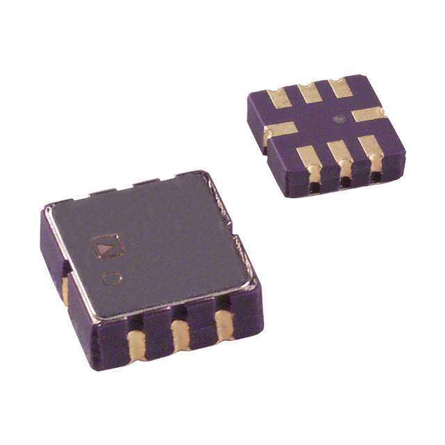
ICGOO电子元器件商城为您提供AD22282-A-R2由Analog设计生产,在icgoo商城现货销售,并且可以通过原厂、代理商等渠道进行代购。 AD22282-A-R2价格参考。AnalogAD22282-A-R2封装/规格:运动传感器 - 加速计, Accelerometer X Axis ±120g 400Hz 8-CLCC (5x5)。您可以下载AD22282-A-R2参考资料、Datasheet数据手册功能说明书,资料中有AD22282-A-R2 详细功能的应用电路图电压和使用方法及教程。
AD22282-A-R2 是由 Analog Devices Inc.(ADI)生产的一款高性能 MEMS 加速度传感器,属于运动传感器中的三轴数字加速度计。该器件具备高精度、低噪声和宽频率响应特性,适用于对振动、冲击和运动状态监测要求较高的工业与高端应用场景。

典型应用包括:工业自动化设备中的状态监控与预测性维护,如电机、泵和风机的振动分析;精密仪器中的倾斜检测与动态姿态感知;以及结构健康监测系统,用于桥梁、建筑或大型机械的长期加速度数据采集。此外,该传感器也可应用于测试与测量设备、惯性导航辅助系统及高端消费类机器人中,提供可靠的运动反馈。

AD22282-A-R2 采用小型化封装,具备良好的温度稳定性和抗干扰能力,适合在复杂电磁环境和宽温条件下稳定运行。其数字输出接口(如SPI/I²C)便于与微控制器或数据采集系统集成,提升系统设计灵活性。总体而言,该型号广泛服务于需要高可靠性与精准运动感知的工业与技术领域。
| 参数 | 数值 |
| 产品目录 | |
| 描述 | IC ACCELER 120G SNGL-AXIS 8CLCC加速计 Single AxisHigh-g |
| 产品分类 | 加速计运动与定位传感器 |
| 品牌 | Analog Devices |
| 产品手册 | |
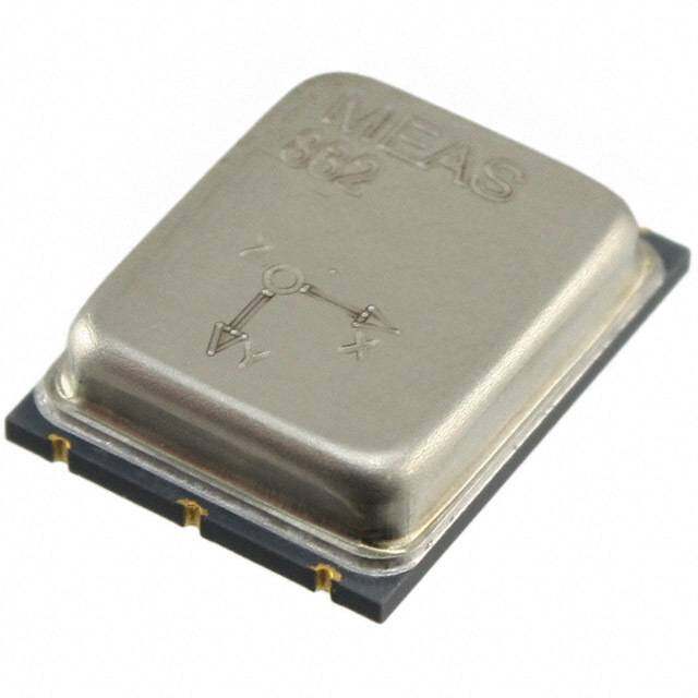
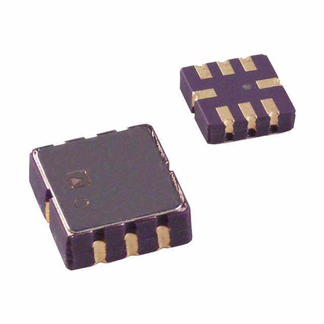
| 产品图片 |
|
| rohs | RoHS 合规性豁免无铅 / 符合限制有害物质指令(RoHS)规范要求 |
| 产品系列 | 加速计,Analog Devices AD22282-A-R2iMEMS® |
| 数据手册 | |
| 产品型号 | AD22282-A-R2 |
| 产品目录页面 | |
| 产品种类 | 加速计 |
| 传感轴 | Single |
| 供应商器件封装 | 8-CLCC(5x5) |
| 其它名称 | AD22282-A-R2DKR |
| 分辨率 | - |
| 加速 | 120 g |
| 加速度范围 | ±120g |
| 商标 | Analog Devices |
| 安装类型 | 表面贴装 |
| 安装风格 | SMD/SMT |
| 封装 | Reel |
| 封装/外壳 | 8-CLCC |
| 封装/箱体 | LCC-8 |
| 工厂包装数量 | 250 |
| 带宽 | 400Hz |
| 接口 | - |
| 最大工作温度 | + 125 C |
| 最小工作温度 | - 40 C |
| 标准包装 | 1 |
| 灵敏度 | 18 mV/g |
| 电压-电源 | 4.75 V ~ 5.25 V |
| 电源电压-最大 | 6 V |
| 电源电压-最小 | 3.5 V |
| 电源电流 | 1.5 uA |
| 系列 | ADXL193 |
| 视频文件 | http://www.digikey.cn/classic/video.aspx?PlayerID=1364138032001&width=640&height=505&videoID=2245193160001http://www.digikey.cn/classic/video.aspx?PlayerID=1364138032001&width=640&height=505&videoID=2245193171001http://www.digikey.cn/classic/video.aspx?PlayerID=1364138032001&width=640&height=505&videoID=2245193170001http://www.digikey.cn/classic/video.aspx?PlayerID=1364138032001&width=640&height=505&videoID=2245193161001http://www.digikey.cn/classic/video.aspx?PlayerID=1364138032001&width=640&height=505&videoID=2245193172001 |
| 轴 | X 或 Y |
| 输出类型 | Analog |


- 商务部:美国ITC正式对集成电路等产品启动337调查
- 曝三星4nm工艺存在良率问题 高通将骁龙8 Gen1或转产台积电
- 太阳诱电将投资9.5亿元在常州建新厂生产MLCC 预计2023年完工
- 英特尔发布欧洲新工厂建设计划 深化IDM 2.0 战略
- 台积电先进制程称霸业界 有大客户加持明年业绩稳了
- 达到5530亿美元!SIA预计今年全球半导体销售额将创下新高
- 英特尔拟将自动驾驶子公司Mobileye上市 估值或超500亿美元
- 三星加码芯片和SET,合并消费电子和移动部门,撤换高东真等 CEO
- 三星电子宣布重大人事变动 还合并消费电子和移动部门
- 海关总署:前11个月进口集成电路产品价值2.52万亿元 增长14.8%

PDF Datasheet 数据手册内容提取
Single-Axis, High-g, iMEMS® Accelerometers ADXL193 FEATURES GENERAL DESCRIPTION Complete acceleration measurement system on a The ADXL193 is a low power, complete single-axis single monolithic IC accelerometer with signal conditioned voltage outputs that are Available in ±120 g or ±250 g output full-scale ranges all on a single monolithic IC. This product measures Full differential sensor and circuitry for high resistance acceleration with a full-scale range of ±120 g or ±250 g to EMI/RFI (minimum). It can also measure boEth dynamic acceleration Environmentally robust packaging (vibration) and static acceleration (gravity). Complete mechanical and electrical self-test on The ADXL193 is a fourth-generation surface micromachined digital command iMEMS® accelerometer Tfrom ADI with enhanced performance Output ratiometric to supply and lower cost. Designed for use in front and side impact airbag Sensitive axes in the plane of the chip applications, this product also provides a complete cost- High linearity (0.2% of full scale) effective solution useful for a wide variety of other applications. Frequency response down to dc E Low noise The ADXL193 is temperature stable and accurate over the Low power consumption (1.5 mA) automotive temperature range, with a self-test feature that fully Tight sensitivity tolerance and 0 g offset capability exercises all the mechanical and electrical elements of the L Largest available prefilter clipping headroom sensor with a digital signal applied to a single pin. 400 Hz, 2-pole Bessel filter The ADXL193 is available in a 5 mm × 5 mm × 2 mm, Single-supply operation 8-terminal ceramic LCC package. O Compatible with Sn/Pb and Pb-free solder processes Qualified for automotive applications APPLICATIONS Vibration monitoring and control S Vehicle collision sensing Shock detection B FUNCTIONAL BLOCK DIAGRAM O VS ADXL193 TIMING VDD GENERATOR VDD2 400Hz DIFFERENTIAL DEMOD EXC SENSOR AMP BESSEL XOUT FILTER SELF-TEST 05366-001 Figure 1. Rev. B Information furnished by Analog Devices is believed to be accurate and reliable. However, no responsibility is assumed by Analog Devices for its use, nor for any infringements of patents or other One Technology Way, P.O. Box 9106, Norwood, MA 02062-9106, U.S.A. rights of third parties that may result from its use. Specifications subject to change without notice. No license is granted by implication or otherwise under any patent or patent rights of Analog Devices. Tel: 781.329.4700 www.analog.com Trademarks and registered trademarks are the property of their respective owners. Fax: 781.461.3113 ©2010 Analog Devices, Inc. All rights reserved.
ADXL193 TABLE OF CONTENTS Features .............................................................................................. 1 Applications ........................................................................................8 Applications ....................................................................................... 1 Power Supply Decoupling ............................................................8 General Description ......................................................................... 1 Self-Test ..........................................................................................8 Functional Block Diagram .............................................................. 1 Clock Frequency Supply Response .............................................8 Specifications ..................................................................................... 3 Signal Distortion ...........................................................................8 Absolute Maximum Ratings ............................................................ 4 Outline Dimensions ..........................................................................9 ESD Caution .................................................................................. 4 ADXL193 Ordering Guide ...................E........................................9 Pin Configuration and Function Descriptions ............................. 5 Automotive Products ....................................................................9 Theory of Operation ........................................................................ 7 T REVISION HISTORY 8/10—Rev. A to Rev. B E Updated Format .................................................................. Universal Change to Features Section ............................................................. 1 Updated Outline Dimensions ......................................................... 9 L Changes to Ordering Guide ............................................................ 9 Added Automotive Products Section ............................................ 9 O 5/05—Rev. 0 to Rev. A S B O Rev. B | Page 2 of 12
ADXL193 SPECIFICATIONS1 At T = −40°C to +105°C, 5.0 V dc ± 5%, acceleration = 0 g; unless otherwise noted. A Table 1. Model No. AD22282 Model No. AD22283 Parameter Conditions Min Typ Max Min Typ Max Unit SENSOR Output Full-Scale Range I ≤ ±100 μA 120 250 g OUT Nonlinearity 0.2 2 0.2 2 % Package Alignment Error 1 1 E Degree Cross-Axis Sensitivity −5 +5 −5 +5 % Resonant Frequency 24 24 kHz Sensitivity, Ratiometric V = 5 V, 100 Hz 17.1 18 18.9 7.6 8 8.4 mV/g DD T (Over Temperature) OFFSET Zero-g Output Voltage V − V /2, V = 5 V −125 +125 −100 +100 mV OUT DD DD (Over Temperature)2 E NOISE Noise Density 10 Hz − 400 Hz, 5 V 3 10 5 15 mg/√Hz Clock Noise 5 5 mV p-p L FREQUENCY RESPONSE Two-pole Bessel −3 dB Frequency 360 400 440 360 400 440 Hz −3 dB Frequency Drift 25°C to T or T 2 2 Hz MIN MAX O SELF-TEST Output Change V = 5 V 400 500 600 200 250 300 mV DD (Cube vs. V )3 DD Logic Input High V = 5 V 3.5 3.5 V DD Logic Input Low VDD = 5 V S 1 1 V Input Resistance Pull-down resistor to GND 30 50 30 50 kΩ OUTPUT AMPLIFIER Output Voltage Swing I = ±400 μA 0.25 V − 0.25 0.25 V − 0.25 V OUT DD DD B Capacitive Load Drive 1000 1000 pF PREFILTER HEADROOM 800 1400 g CFSR @ 400 kHz 2 1.5 V/V POWER SUPPLY (V ) 4.75 5.25 4.75 5.25 V DD O Functional Range 3.5 6 3.5 6 V Quiescent Supply Current V = 5 V 1.5 2 1.5 2 mA DD TEMPERATURE RANGE −40 +125 −40 +125 °C 1 All minimum and maximum specifications are guaranteed. Typical specifications are not guaranteed. 2 Zero g output is ratiometric. 3 Self-test output at VDD = (Self-Test Output at 5 V) × (VDD/5 V)3. Rev. B | Page 3 of 12
ADXL193 ABSOLUTE MAXIMUM RATINGS Table 2. Stresses above those listed under Absolute Maximum Ratings Parameter Rating may cause permanent damage to the device. This is a stress Acceleration (Any Axis, Unpowered) 4,000 g rating only; functional operation of the device at these or any Acceleration (Any Axis, Powered) 4,000 g other conditions above those indicated in the operational V −0.3 V to +7.0 V S section of this specification is not implied. Exposure to absolute All Other Pins (COM − 0.3 V) to maximum rating conditions for extended periods may affect (V + 0.3 V) S device reliability. E Output Short-Circuit Duration Indefinite (Any Pin to Common) ESD CAUTION Operating Temperature Range −65°C to +150°C Storage Temperature −65°C to +150°C T E L O S B O Rev. B | Page 4 of 12
ADXL193 PIN CONFIGURATION AND FUNCTION DESCRIPTIONS VDD2 8 NC 1 7 VDD ADXL193 NC 2 TOP VIEW 6 XOUT (Not to Scale) COM 3 5 NC 4 E NC = NO CONNESCTT 05366-002 Figure 2. Pin Configuration T Table 3. Pin Function Descriptions Pin No. Mnemonic Description E 1 NC Do Not Connect 2 NC Do Not Connect 3 COM Common 4 ST LSelf-Test 5 NC Do Not Connect 6 X X Channel Output OUT 7 VDD O 3.5 V to 6 V 8 V 3.5 V to 6 V DD2 S B O Rev. B | Page 5 of 12
ADXL193 CRITICAL ZONE TP tP TL TO TP RAMP-UP URETL TSMAX tL T A ER TSMIN P M E T t PREHSEAT RAMP-DOWN 05366-003 E t25°C TO PEAK TIME Figure 3. Recommended Soldering Profile T Table 4. Recommended Soldering Profile Profile Feature Sn63/Pb37 Pb-Free E AVERAGE RAMP RATE (T TO T) 3°C/s max 3°C/s max L P PREHEAT Minimum Temperature (T ) 100°C 150°C SMIN Maximum Temperature (T ) 15L0°C 200°C SMAX TIME (T TO T ), t 60 s − 120 s 60 s − 150 s SMIN SMAX S T TO T SMAX L Ramp-Up Rate O 3°C/s 3°C/s TIME MAINTAINED ABOVE LIQUIDOUS (T) L Liquidous Temperature (T) 183°C 217°C L Time (t) 60 s − 150 s 60 s − 150 s L PEAK TEMPERATURE (TP) S 240°C + 0°C/−5°C 260°C + 0°C/−5°C TIME WITHIN 5°C OF ACTUAL PEAK TEMPERATURE (t) 10 s − 30 s 20 s − 40 s P RAMP-DOWN RATE 6°C/s max 6°C/s max TIME 25°C TO PEAK TEMPERATURE 6 min max 8 min max B PIN 8 O XXXXX XXXX XOUT = 2.482V 22282 XOUT = 2.500V XXXXXXXXX 22282 22282 XXXXXXXXX XOUT = 2.500V 28222 XXXX XOUT = 2.518V XXXXX XOUT = 2.500V EARTH'S SURFACE 05366-004 Figure 4. Output Response vs. Orientation Rev. B | Page 6 of 12
ADXL193 THEORY OF OPERATION The ADXL193 provides a fully differential sensor structure and ANCHOR circuit path, resulting in the industry’s highest resistance to EMI/RFI effects. This latest generation uses electrical feedback MOVABLE with zero-force feedback for improved accuracy and stability. PLATE FRAME CAPACITORS The sensor resonant frequency is significantly higher than the UNIT signal bandwidth set by the on-chip filter, avoiding the signal TION SENCSEINLGL FPILXAETDES analysis problems caused by resonant peaks near the signal A R E bandwidth. L CE UNIT Figure 5 is a simplified view of one of the differential sensor AC MOVING E FCOERLLCING PLATE elements. Each sensor includes several differential capacitor unit cells. Each cell is composed of fixed plates attached tDoi sthpela scuebmsetrnatt eo fa tnhde mfroamvaeb lceh palnagteess athttea cdhifefder teon tthiael fcraapmacei.t ance, T ANCHOR 05366-005 which is measured by the on-chip circuitry. Figure 5. Simplified View of Sensor Under Acceleration Complementary 400 kHz square waves drive the fixed plates. E Electrical feedback adjusts the amplitudes of the square waves such that the ac signal on the moving plates is 0. The feedback signal is linearly proportional to the applied acceleration. This unique feedback technique ensures that there is no net L electrostatic force applied to the sensor. The differential feedback control signal is also applied to the input of the filter, where it is filtered and converted to a single-ended signal. O S B O Rev. B | Page 7 of 12
ADXL193 APPLICATIONS POWER SUPPLY DECOUPLING If the difference frequency is outside of the signal bandwidth, the filter attenuates it. However, both the power supply clock For most applications, a single 0.1 μF capacitor, C , adequately DC and the accelerometer clock may vary with time or temperature, decouples the accelerometer from noise on the power supply. which can cause the interference signal to appear in the output However, in some cases, particularly where noise is present at filter bandwidth. the 400 kHz internal clock frequency (or any harmonic The ADXL193 addresses this issue in two ways. First, the high thereof), noise on the supply can cause interference on the clock frequency eases the task of choosing a power supply clock ADXL193’s output. If additional decoupling is needed, a 50 Ω frequency such that the difference between it and the accelero- (or smaller) resistor or ferrite bead can be inserted in the supply meter clock remains well outside of the fEilter bandwidth. line. Additionally, a larger bulk bypass capacitor (in the 1 μF to Second, the ADXL193 is the only micromachined accelerometer 4.7 μF range) can be added in parallel to C . DC to have a fully differential signal path, including differential SELF-TEST sensors. The differential sensors eliminate most of the power T The fixed fingers in the forcing cells are normally kept at the supply noise before it reaches the demodulator. Good high same potential as that of the movable frame. When the self-test frequency supply bypassing, such as a ceramic capacitor close to digital input is activated, the voltage on the fixed fingers on one the supply pins, also minimizes the amount of interference. E side of the moving plate in the forcing cells is changed. This The clock frequency supply response (CFSR) is the ratio of the creates an attractive electrostatic force, which causes the frame response at V to the noise on the power supply near the OUT to move toward those fixed fingers. The entire signal channel is accelerometer clock frequency. A CFSR of 3 means that the active; therefore, the sensor displacement causes a change in signal aLt V is 3× the amplitude of an excitation signal at V OUT DD V . The ADXL193’s self-test function is a comprehensive OUT near the accelerometer internal clock frequency. This is method of verifying the operation of the accelerometer. analogous to the power supply response, except that the Because electrostatic force is independent of the polarity of the Ostimulus and the response are at different frequencies. The voltage across capacitor plates, a positive voltage is applied in ADXL193’s CFSR is 10× better than a typical single-ended half of the forcing cells, and its complement in the other half of accelerometer system. the forcing cells. Activating self-test causes a step function force SIGNAL DISTORTION to be applied to the sensor, while the capacitive coupling term is S Signals from crashes and other events may contain high canceled. The ADXL193 has improved self-test functionality, amplitude, high frequency components. These components including excellent transient response and high speed switching contain very little useful information and are reduced by the capability. Arbitrary force waveforms can be applied to the sensor by modulating the self-test input, suchB as test signals to 2-pole Bessel filter at the output of the accelerometer. However, if the signal saturates at any point, the accelerometer output measure the system frequency response, or even crash signals to does not look like a filtered version of the acceleration signal. verify algorithms within the limits of the self-test swing. The signal may saturate anywhere before the filter. For example, if The ST pin should never be exposed to voltages greater than O the resonant frequency of the sensor is low, the displacement per V + 0.3 V. If this cannot be guaranteed due to the system S unit acceleration is high. The sensor may reach the mechanical design (for instance, if there are multiple supply voltages), then limit of travel if the applied acceleration is high enough. This can a low V clamping diode between ST and V is recommended. F S be remedied by locating the accelerometer where it does not see CLOCK FREQUENCY SUPPLY RESPONSE high values of acceleration and by using a higher resonant In any clocked system, power supply noise near the clock frequency sensor, such as the ADXL193. frequency may have consequences at other frequencies. An Also, the electronics may saturate in an overload condition internal clock typically controls the sensor excitation and the between the sensor output and the filter input. Ensuring that signal demodulator for micromachined accelerometers. internal circuit nodes operate linearly to at least several times If the power supply contains high frequency spikes, they may be the full-scale acceleration value can minimize electrical demodulated and interpreted as an acceleration signal. A signal saturation. The ADXL193 circuit is linear to approximately 8× appears as the difference between the noise frequency and the full scale. demodulator frequency. If the power supply spikes are 100 Hz away from the demodulator clock, there is an output term at 100 Hz. If the power supply clock is at exactly the same frequency as the accelerometer clock, the term appears as an offset. Rev. B | Page 8 of 12
ADXL193 OUTLINE DIMENSIONS 0.030 (PLATINGOPTION1, 0.025 SEEDETAILA FOROPTION2) 0.203 0.087 0.054 0.020 0.028 0.197SQ 0.020 0.078 0.050 0.020DIA 0.193 0.015 0.069 0.046 0.012 0.010 (R4PLCS) 7 1 0.180 0.106 0.177SQ 0.075REF 0.100 0.174 R0.008 0.094 (8PLCS) E 5 3 R0.008 TOPVIEW 0.008 BOTTOMVIEW (4PLCS) 0.006 0.077 0.004 0.070 0.019SQ 0.063 (ODPETTIAOILNA2) T 05-21-2010-D Figure 6. 8-Terminal Ceramic Leadless Chip Carrier [LCC] E (E-8-1) Dimensions shown in inches ADXL193 ORDERING GUIDE Parts L per Measurement Specified Temperature Package Model1, 2, 3 Reel Range Voltage (V) Range Package Description Option AD22282-A-R2 250 ±120 g 5 −40°C to +125°C 8-Terminal Ceramic Leadless Chip Carrier E-8-1 O AD22282-A 3,000 ±120 g 5 −40°C to +125°C 8-Terminal Ceramic Leadless Chip Carrier E-8-1 ADW22282ZD 3,000 ±120 g 5 −40°C to +125°C 8-Terminal Ceramic Leadless Chip Carrier E-8-1 ADW22282ZD-RL7 250 ±120 g 5 −40°C to +125°C 8-Terminal Ceramic Leadless Chip Carrier E-8-1 AD22283-B-R2 250 ±250 g 5 −40°C to +125°C 8-Terminal Ceramic Leadless Chip Carrier E-8-1 S AD22283-B 3,000 ±250 g 5 −40°C to +125°C 8-Terminal Ceramic Leadless Chip Carrier E-8-1 ADW22283ZE 3,000 ±250 g 5 −40°C to +125°C 8-Terminal Ceramic Leadless Chip Carrier E-8-1 ADW22283ZE-RL7 250 ±250 g 5 −40°C to +125°C 8-Terminal Ceramic Leadless Chip Carrier E-8-1 B 1 All models are on tape and reel and are RoHS compliant parts. 2 Z = RoHS Compliant Part. 3 W = Qualified for Automotive Applications. AUTOMOTIVE PRODUOCTS The ADW22282 and ADW22283 models are available with controlled manufacturing to support the quality and reliability requirements of automotive applications. Note that these automotive models may have specifications that differ from the commercial models; therefore, designers should review the Specifications section of this data sheet carefully. Only the automotive grade products shown are available for use in automotive applications. Contact your local Analog Devices account representative for specific product ordering information and to obtain the specific Automotive Reliability reports for these models. Rev. B | Page 9 of 12
ADXL193 NOTES E T E L O S B O Rev. B | Page 10 of 12
ADXL193 NOTES E T E L O S B O Rev. B | Page 11 of 12
ADXL193 NOTES E T E L O S B O ©2010 Analog Devices, Inc. All rights reserved. Trademarks and registered trademarks are the property of their respective owners. D05366-0-8/10(B) Rev. B | Page 12 of 12