ICGOO在线商城 > 传感器,变送器 > 运动传感器 - 加速计 > ADXL203CE-REEL
 Datasheet下载
- 型号: ADXL203CE-REEL
- 制造商: Analog
- 库位|库存: xxxx|xxxx
- 要求:
| 数量阶梯 | 香港交货 | 国内含税 |
| +xxxx | $xxxx | ¥xxxx |
查看当月历史价格
查看今年历史价格
ADXL203CE-REEL产品简介:
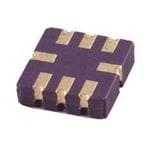
ICGOO电子元器件商城为您提供ADXL203CE-REEL由Analog设计生产,在icgoo商城现货销售,并且可以通过原厂、代理商等渠道进行代购。 ADXL203CE-REEL价格参考¥67.00-¥80.40。AnalogADXL203CE-REEL封装/规格:运动传感器 - 加速计, Accelerometer X, Y Axis ±1.7g 0.5Hz ~ 2.5kHz 8-LCC (5x5)。您可以下载ADXL203CE-REEL参考资料、Datasheet数据手册功能说明书,资料中有ADXL203CE-REEL 详细功能的应用电路图电压和使用方法及教程。
ADXL203CE-REEL是Analog Devices Inc.生产的一款双轴加速度传感器,属于运动传感器中的加速计类别。该器件具有高精度、低功耗和宽工作温度范围等特点,广泛应用于对稳定性和可靠性要求较高的工业与消费类电子领域。

其典型应用场景包括:工业仪器中的倾斜检测与振动监测,用于确保设备在安全角度范围内运行;平台稳定系统,如摄像机云台或天线控制系统,通过实时感知加速度变化实现自动调平;汽车电子中的车身动态监控,可用于车辆安全系统中的碰撞检测辅助功能;此外,在建筑与结构健康监测中,ADXL202CE-REEL也常被用于桥梁、塔架等基础设施的微小振动与位移检测。

由于其采用小型化表面贴装封装并支持全温区工作,该传感器也适用于空间受限且环境复杂的嵌入式系统。同时,它还可用于消费类设备中的运动感应功能,如高端导航设备或便携式测量工具。

总之,ADXL203CE-REEL凭借其稳定的性能和较强的抗干扰能力,广泛服务于工业控制、汽车安全、通信设备和精密仪器等多个领域,是实现精确加速度测量的理想选择。
| 参数 | 数值 |
| 产品目录 | |
| 描述 | IC ACCELEROMETER DUAL-AXIS 8CLCC |
| 产品分类 | 加速计 |
| 品牌 | Analog Devices Inc |
| 数据手册 | |
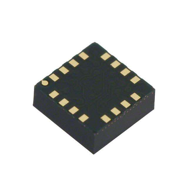
| 产品图片 |
|
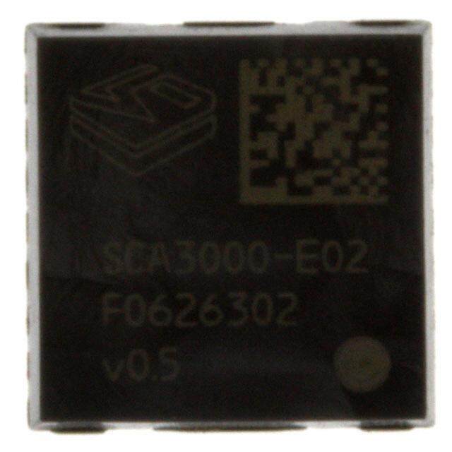
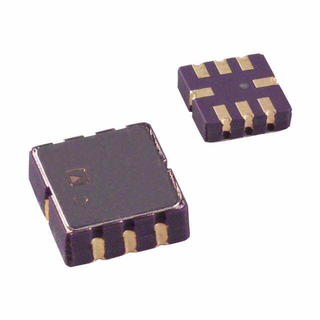
| 产品型号 | ADXL203CE-REEL |
| rohs | 无铅 / 符合限制有害物质指令(RoHS)规范要求 |
| 产品系列 | iMEMS® |
| 供应商器件封装 | 8-CLCC(5x5) |
| 其它名称 | ADXL203CE-REELCT |
| 加速度范围 | ±1.7g |
| 参考设计库 | http://www.digikey.com/rdl/4294959886/4294959846/1022 |
| 安装类型 | 表面贴装 |
| 封装/外壳 | 8-CLCC |
| 带宽 | 0.5Hz ~ 2.5kHz 可选 |
| 接口 | - |
| 标准包装 | 1 |
| 灵敏度 | 1000mV/g |
| 电压-电源 | 3 V ~ 6 V |
| 视频文件 | http://www.digikey.cn/classic/video.aspx?PlayerID=1364138032001&width=640&height=505&videoID=2245193160001http://www.digikey.cn/classic/video.aspx?PlayerID=1364138032001&width=640&height=505&videoID=2245193171001http://www.digikey.cn/classic/video.aspx?PlayerID=1364138032001&width=640&height=505&videoID=2245193170001http://www.digikey.cn/classic/video.aspx?PlayerID=1364138032001&width=640&height=505&videoID=2245193161001http://www.digikey.cn/classic/video.aspx?PlayerID=1364138032001&width=640&height=505&videoID=2245193172001 |
| 轴 | X,Y |
| 输出类型 | 模拟 |
| 配用 | /product-detail/zh/ADXL203EB/ADXL203EB-ND/665382 |


- 商务部:美国ITC正式对集成电路等产品启动337调查
- 曝三星4nm工艺存在良率问题 高通将骁龙8 Gen1或转产台积电
- 太阳诱电将投资9.5亿元在常州建新厂生产MLCC 预计2023年完工
- 英特尔发布欧洲新工厂建设计划 深化IDM 2.0 战略
- 台积电先进制程称霸业界 有大客户加持明年业绩稳了
- 达到5530亿美元!SIA预计今年全球半导体销售额将创下新高
- 英特尔拟将自动驾驶子公司Mobileye上市 估值或超500亿美元
- 三星加码芯片和SET,合并消费电子和移动部门,撤换高东真等 CEO
- 三星电子宣布重大人事变动 还合并消费电子和移动部门
- 海关总署:前11个月进口集成电路产品价值2.52万亿元 增长14.8%

PDF Datasheet 数据手册内容提取
Precision ±1.7 g, ±5 g, ±18 g Single-/ Dual-Axis iMEMS® Accelerometer Data Sheet ADXL103/ADXL203 FEATURES GENERAL DESCRIPTION High performance, single-/dual-axis accelerometer on The ADXL103/ADXL203 are high precision, low power, complete a single IC chip single- and dual-axis accelerometers with signal conditioned 5 mm × 5 mm × 2 mm LCC package voltage outputs, all on a single, monolithic IC. The ADXL103/ 1 mg resolution at 60 Hz ADXL203 measure acceleration with a full-scale range of ±1.7 g, Low power: 700 μA at VS = 5 V (typical) ±5 g, or ±18 g. The ADXL103/ADXL203 can measure both High zero g bias stability dynamic acceleration (for example, vibration) and static High sensitivity accuracy acceleration (for example, gravity). −40°C to +125°C temperature range The typical noise floor is 110 μg/√Hz, allowing signals below 1 mg X and Y axes aligned to within 0.1° (typical) (0.06° of inclination) to be resolved in tilt sensing applications Bandwidth adjustment with a single capacitor using narrow bandwidths (<60 Hz). Single-supply operation 3500 g shock survival The user selects the bandwidth of the accelerometer using RoHS compliant Capacitor CX and Capacitor CY at the XOUT and YOUT pins. Compatible with Sn/Pb- and Pb-free solder processes Bandwidths of 0.5 Hz to 2.5 kHz can be selected to suit the application. APPLICATIONS The ADXL103 and ADXL203 are available in a 5 mm × 5 mm × Platform stabilization/leveling 2 mm, 8-terminal ceramic LCC package. Navigation Alarms and motion detectors High accuracy, 2-axis tilt sensing Vibration monitoring and compensation Abuse event detection FUNCTIONAL BLOCK DIAGRAMS +5V +5V VS VS ADXL103 ADXL203 CDC AC DEMOD OUTPUT CDC AC DEMOD OUTPUT OUTPUT AMP AMP AMP AMP AMP SENSOR SENSOR RFILT RFILT RFILT 32kΩ 32kΩ 32kΩ COM ST XOUT COM ST YOUT XOUT CX CY CX 03757-001 Figure 1. Rev. F Document Feedback Information furnished by Analog Devices is believed to be accurate and reliable. However, no responsibility is assumed by Analog Devices for its use, nor for any infringements of patents or other One Technology Way, P.O. Box 9106, Norwood, MA 02062-9106, U.S.A. rights of third parties that may result from its use. Specifications subject to change without notice. No license is granted by implication or otherwise under any patent or patent rights of Analog Devices. Tel: 781.329.4700 ©2004–2018 Analog Devices, Inc. All rights reserved. Trademarks and registered trademarks are the property of their respective owners. Technical Support www.analog.com
ADXL103/ADXL203 Data Sheet TABLE OF CONTENTS Features .............................................................................................. 1 Theory of Operation ...................................................................... 13 Applications ....................................................................................... 1 Performance ................................................................................ 13 General Description ......................................................................... 1 Applications Information .............................................................. 14 Functional Block Diagrams ............................................................. 1 Power Supply Decoupling ......................................................... 14 Revision History ............................................................................... 2 Setting the Bandwidth Using C and C ................................. 14 X Y Specifications ..................................................................................... 3 Self Test ........................................................................................ 14 Absolute Maximum Ratings ............................................................ 4 Design Trade-Offs for Selecting Filter Characteristics: The ESD Caution .................................................................................. 4 Noise/Bandwidth Trade-Off ..................................................... 14 Pin Configurations and Function Descriptions ........................... 5 Using the ADXL103/ADXL203 with Operating Voltages Other than 5 V ............................................................................ 15 Typical Performance Characteristics ............................................. 6 Using the ADXL203 as a Dual-Axis Tilt Sensor ........................ 15 ADXL103 and ADXL203 .............................................................. 6 Outline Dimensions ....................................................................... 16 AD22293 ........................................................................................ 9 Ordering Guide .......................................................................... 16 AD22035 and AD22037 ............................................................ 10 All Models ................................................................................... 12 REVISION HISTORY 5/2018—Rev. E to Rev. F 4/2010—Rev. A to Rev. B Changes to Features Section and Applications Section ............... 1 Changes to Features Section ............................................................ 1 Changes to Noise Parameter, Table 1 ............................................. 3 Updated Outline Dimensions ....................................................... 12 Changes to Ordering Guide .......................................................... 16 Changes to Ordering Guide .......................................................... 12 Deleted Automotive Products Section ......................................... 16 2/2006—Rev. 0 to Rev. A 1/2014—Rev. D to Rev. E Changes to Features .......................................................................... 1 Changes to Ordering Guide .......................................................... 16 Changes to Table 1 ............................................................................. 3 Changes to Figure 2 ........................................................................... 4 9/2011—Rev. C to Rev. D Changes to Figure 3 and Figure 4 .................................................... 5 Added AD22293, AD22035, and AD22037 ............... Throughout Changes to the Performance Section .............................................. 9 Changes to Application Section and General Description Section ................................................................................................ 1 4/2004—Revision 0: Initial Version Changes to Table 1 ............................................................................ 3 Deleted Figure 13 and Figure 14: Renumbered Sequentially ..... 7 Deleted Figure 17 and Figure 22 ..................................................... 8 Added Figure 19 to Figure 24; Renumbered Sequentially .......... 9 Added Figure 25 to Figure 34........................................................ 10 Added All Models Section, Figure 35 to Figure 38 .................... 12 Changes to Figure 39 ...................................................................... 13 Changes to Ordering Guide .......................................................... 16 Changes to Automotive Products Section ................................... 16 5/2010—Rev. B to Rev. C Changes to Figure 24 Caption ....................................................... 12 Added Automotive Products Section........................................... 12 Rev. F | Page 2 of 16
Data Sheet ADXL103/ADXL203 SPECIFICATIONS T = −40°C to +125°C, V = 5 V, C = C = 0.1 µF, acceleration = 0 g, unless otherwise noted. All minimum and maximum specifications A S X Y are guaranteed. All typical specifications are not guaranteed. Table 1. ADXL103/ADXL203 AD22293 AD22035/AD22037 Parameter Test Conditions Min Typ Max Min Typ Max Min Typ Max Unit SENSOR Each axis Measurement Range1 ±1.7 ±5 ±6 ±18 g Nonlinearity % of full scale ±0.2 ±1.25 ±0.2 ±1.25 ±0.2 ±1.25 % Package Alignment Error ±1 ±1 ±1 Degrees Alignment Error (ADXL203) X to Y sensor ±0.1 ±0.1 ±0.1 Degrees Cross-Axis Sensitivity ±1.5 ±3 ±1.5 ±3 ±1.5 ±3 % SENSITIVITY (RATIOMETRIC)2 Each axis Sensitivity at X , Y V = 5 V 960 1000 1040 293 312 331 94 100 106 mV/g OUT OUT S Sensitivity Change Due to V = 5 V ±0.3 ±0.3 ±0.3 % S Temperature3 ZERO g BIAS LEVEL (RATIOMETRIC) Each axis 0 g Voltage at X , Y V = 5 V 2.4 2.5 2.6 2.4 2.5 2.6 2.4 2.5 2.6 V OUT OUT S Initial 0 g Output Deviation V = 5 V, 25°C ±25 ±50 ±125 mg S from Ideal 0 g Offset vs. Temperature ±0.1 ±0.8 ±0.3 ±1.8 ±1 mg/°C NOISE Output Noise 1 3 0.4 0.2 mV rms Noise Density 110 130 230 µg/√Hz rms FREQUENCY RESPONSE4 C , C Range5 0.002 10 0.002 10 0.002 10 µF X Y R Tolerance 24 32 40 24 32 40 24 32 40 kΩ FILT Sensor Resonant Frequency 5.5 5.5 5.5 kHz SELF TEST6 Logic Input Low 1 1 1 V Logic Input High 4 4 4 V ST Input Resistance to GND 30 50 30 50 30 50 kΩ Output Change at X , Y ST 0 to ST 1 450 750 1100 125 250 375 60 80 100 mV OUT OUT OUTPUT AMPLIFIER Output Swing Low No load 0.05 0.2 0.05 0.2 0.05 0.2 V Output Swing High No load 4.5 4.8 4.5 4.8 4.5 4.8 V POWER SUPPLY (V ) DD Operating Voltage Range 3 6 3 6 3 6 V Quiescent Supply Current 0.7 1.1 0.7 1.1 0.7 1.1 mA Turn-On Time7 20 20 20 ms 1 Guaranteed by measurement of initial offset and sensitivity. 2 Sensitivity is essentially ratiometric to VS. For VS = 4.75 V to 5.25 V, sensitivity is 186 mV/V/g to 215 mV/V/g. 3 Defined as the output change from ambient-to-maximum temperature or ambient-to-minimum temperature. 4 Actual frequency response controlled by user-supplied external capacitor (CX, CY). 5 Bandwidth = 1/(2 × π × 32 kΩ × C). For CX, CY = 0.002 µF, bandwidth = 2500 Hz. For CX, CY = 10 µF, bandwidth = 0.5 Hz. Minimum/maximum values are not tested. 6 Self-test response changes cubically with VS. 7 Larger values of CX, CY increase turn-on time. Turn-on time is approximately 160 × CX or CY + 4 ms, where CX, CY are in µF. Rev. F | Page 3 of 16
ADXL103/ADXL203 Data Sheet ABSOLUTE MAXIMUM RATINGS Table 3. Package Characteristics Table 2. Package Type θ θ Device Weight Parameter Rating JA JC 8-Terminal Ceramic LCC 120°C/W 20°C/W <1.0 gram Acceleration (Any Axis, Unpowered) 3500 g Acceleration (Any Axis, Powered) 3500 g Drop Test (Concrete Surface) 1.2 m ESD CAUTION V −0.3 V to +7.0 V S All Other Pins (COM − 0.3 V) to (V + 0.3 V) S Output Short-Circuit Duration Indefinite (Any Pin to Common) Temperature Range (Powered) −55°C to +125°C Temperature Range (Storage) −65°C to +150°C Stresses at or above those listed under Absolute Maximum Ratings may cause permanent damage to the product. This is a stress rating only; functional operation of the product at these or any other conditions above those indicated in the operational section of this specification is not implied. Operation beyond the maximum operating conditions for extended periods may affect product reliability. CRITICAL ZONE TP tP TL TO TP RAMP-UP URETL TSMAX tL T A R PE TSMIN M E T PREtHSEAT RAMP-DOWN 03757-102 t25°C TO PEAK TIME Figure 2. Recommended Soldering Profile Table 4. Solder Profile Parameters Test Condition Profile Feature Sn63/Pb37 Pb-Free Average Ramp Rate (T to T) 3°C/second maximum 3°C/second maximum L P Preheat Minimum Temperature (T ) 100°C 150°C SMIN Maximum Temperature (T ) 150°C 200°C SMAX Time (T to T ) (t) 60 seconds to 120 seconds 60 seconds to 150 seconds SMIN SMAX S T to T SMAX L Ramp-Up Rate 3°C/second 3°C/second Time Maintained Above Liquidous (T) L Liquidous Temperature (T) 183°C 217°C L Time (t) 60 seconds to 150 seconds 60 seconds to 150 seconds L Peak Temperature (T) 240°C + 0°C/−5°C 260°C + 0°C/−5°C P Time Within 5°C of Actual Peak Temperature (t) 10 seconds to 30 seconds 20 seconds to 40 seconds P Ramp-Down Rate 6°C/second maximum 6°C/second maximum Time 25°C to Peak Temperature 6 minutes maximum 8 minutes maximum Rev. F | Page 4 of 16
Data Sheet ADXL103/ADXL203 PIN CONFIGURATIONS AND FUNCTION DESCRIPTIONS ADXL103 ADXL203 TOP VIEW TOP VIEW (Not to Scale) (Not to Scale) VS VS 8 8 ST 1 7 XOUT ST 1 7 XOUT NC 2 +X 6 NC NC 2 +Y 6 YOUT +X COM 3 5 NC COM 3 5 NC N4C 03757-002 N4C 03757-003 NOTES NOTES 1. NC = NO CONNECT. DO NOT CONNECT TO THIS PIN. 1. NC = NO CONNECT. DO NOT CONNECT TO THIS PIN. Figure 3. ADXL103 Pin Configuration Figure 4. ADXL203 Pin Configuration Table 5. ADXL103 Pin Function Descriptions Table 6. ADXL203 Pin Function Descriptions Pin No. Mnemonic Description Pin No. Mnemonic Description 1 ST Self Test 1 ST Self Test 2 NC Do Not Connect 2 NC Do Not Connect 3 COM Common 3 COM Common 4 NC Do Not Connect 4 NC Do Not Connect 5 NC Do Not Connect 5 NC Do Not Connect 6 NC Do Not Connect 6 Y Y Channel Output OUT 7 XOUT X Channel Output 7 XOUT X Channel Output 8 VS 3 V to 6 V 8 VS 3 V to 6 V Rev. F | Page 5 of 16
ADXL103/ADXL203 Data Sheet TYPICAL PERFORMANCE CHARACTERISTICS ADXL103 AND ADXL203 V = 5 V for all graphs, unless otherwise noted. S 25 30 25 20 %) %) N ( N ( O O 20 TI TI A 15 A L L U U OP OP 15 P P OF 10 OF NT NT 10 E E C C R R E 5 E P P 5 0 03757-010 0 03757-013 –0.10 –0.08 –0.06 –0.04 –0.02 0 0.02 0.04 0.06 0.08 0.10 –0.10 –0.08 –0.06 –0.04 –0.02 0 0.02 0.04 0.06 0.08 0.10 ZEROg BIAS (V) ZEROg BIAS (V) Figure 5. X-Axis Zero g Bias Deviation from Ideal at 25°C Figure 8. Y-Axis Zero g Bias Deviation from Ideal at 25°C 30 25 25 %) %) 20 PERCENT OF POPULATION ( 2110505 PERCENT OF POPULATION ( 11505 0 03757-011 0 03757-014 –0.80 –0.70 –0.60 –0.50 –0.40 –0.30 –0.20 –0.10 0 0.10 0.20 0.30 0.40 0.50 0.60 0.70 0.80 –0.80 –0.70 –0.60 –0.50 –0.40 –0.30 –0.20 –0.10 0 0.10 0.20 0.30 0.40 0.50 0.60 0.70 0.80 TEMPERATURE COEFFICIENT (mg/°C) TEMPERATURE COEFFICIENT (mg/°C) Figure 6. X-Axis Zero g Bias Temperature Coefficient Figure 9. Y-Axis Zero g Bias Temperature Coefficient 40 40 35 35 PERCENT OF POPULATION (%) 2231105050 PERCENT OF POPULATION (%)2231105050 05 03757-012 05 03757-015 0.94 0.95 0.96 0.97 0.98 0.99 1.00 1.01 1.02 1.03 1.04 1.05 1.06 0.94 0.95 0.96 0.97 0.98 0.99 1.00 1.01 1.02 1.03 1.04 1.05 1.06 SENSITIVITY (V/g) SENSITIVITY (V/g) Figure 7. X-Axis Sensitivity at 25°C Figure 10. Y-Axis Sensitivity at 25°C Rev. F | Page 6 of 16
Data Sheet ADXL103/ADXL203 2.60 1.03 2.58 1.02 2.56 2.54 1.01 GE (1V/g) 22..5520 VITY (V/g) 1.00 A TI VOLT 22..4486 SENSI 0.99 2.44 0.98 22..4402 03757-004 0.97 03757-016 50 40 30 20 10 0 10 20 30 40 50 60 70 80 90 00 10 20 30 50 40 30 20 10 0 10 20 30 40 50 60 70 80 90 00 10 20 30 – – – – – 1 1 1 1 – – – – – 1 1 1 1 TEMPERATURE (°C) TEMPERATURE (°C) Figure 11. Zero g Bias vs. Temperature; Devices Soldered to PCB Figure 13. Sensitivity vs. Temperature; Devices Soldered to PCB 50 50 45 45 40 40 %) %) N ( 35 N ( 35 O O ATI 30 ATI 30 L L U U OP 25 OP 25 P P OF 20 OF 20 T T EN 15 EN 15 C C R R E 10 E 10 P P 05 03757-007 05 03757-008 60 70 80 90 100 110 120 130 140 150 60 70 80 90 100 110 120 130 140 150 X AXIS NOISE DENSITY (mg/√Hz) Y AXIS NOISE DENSITY (mg/√Hz) Figure 12. X-Axis Noise Density at 25°C Figure 14. Y-Axis Noise Density at 25°C Rev. F | Page 7 of 16
ADXL103/ADXL203 Data Sheet 45 45 40 40 %) 35 %) 35 N ( N ( O 30 O 30 TI TI A A UL 25 UL 25 P P O O F P 20 F P 20 O O NT 15 NT 15 E E C C ER 10 ER 10 P P 05 03757-017 05 03757-019 0.40 0.45 0.50 0.55 0.60 0.65 0.70 0.75 0.80 0.85 0.90 0.95 1.00 0.40 0.45 0.50 0.55 0.60 0.65 0.70 0.75 0.80 0.85 0.90 0.95 1.00 SELF-TEST OUTPUT (V) SELF-TEST OUTPUT (V) Figure 15. X-Axis Self-Test Response at 25°C Figure 17. Y-Axis Self-Test Response at 25°C 0.90 100 0.85 90 5V 80 0.80 %) N ( 70 3V O V/g) 0.75 LATI 60 1 U OLTAGE ( 00..7605 T OF POP 5400 V EN 30 0.60 RC E 20 P 00..5505 03757-103 100 03757-018 –50 –40 –30 –20 –10 0 10TE20MPE30RA40TU50RE 60(°C)70 80 90 100 110 120 130 200 300 400 500 600 700 800 900 1000 CURRENT (µA) Figure 16. Self-Test Response vs. Temperature Figure 18. Supply Current at 25°C Rev. F | Page 8 of 16
Data Sheet ADXL103/ADXL203 AD22293 60 70 60 50 %) %) N ( N ( 50 O O ATI 40 ATI L L U U 40 P P O 30 O P P OF OF 30 T T N 20 N E E C C 20 R R E E P P 10 10 0 0 2.43 2.44 2.45 2.46 2.47 2.48ZER2.49Og2.50 BIA2.51S (V2.52) 2.53 2.54 2.55 2.56 2.57 03757-117 2.43 2.44 2.45 2.46 2.47 2.48ZER2.49Og2.50 BIA2.51S (V2.52) 2.53 2.54 2.55 2.56 2.57 03757-119 Figure 19. X-Axis Zero g Bias at 25°C Figure 22. Y-Axis Zero g Bias at 25°C 25 25 %) 20 %) 20 N ( N ( O O TI TI A A L 15 L 15 U U P P O O P P F F T O 10 T O 10 N N E E C C R R E E P 5 P 5 0 0 –1.2 –1.0 –0.8TEM–0.6PER–0.4ATUR–0.2E CO0EFF0.2ICIEN0.4T (m0.6g/°C)0.8 1.0 1.2 03757-118 –1.2 –1.0 –0.8TEM–0.6PER–0.4ATUR–0.2E CO0EFF0.2ICIEN0.4T (mg0.6/°C)0.8 1.0 1.2 03757-020 Figure 20. X-Axis Zero g Bias Temperature Coefficient Figure 23. Y-Axis Zero g Bias Temperature Coefficient 90 80 80 70 %) 70 %) N ( N ( 60 O O ATI 60 ATI 50 L L PU 50 PU PO PO 40 F 40 F O O T T 30 N 30 N E E C C R R 20 E 20 E P P 10 10 0 0 0.287 0.297 0.307 0.317 SE0.327NSITIV0.337ITY (V0.347/g) 0.357 0.367 0.377 0.387 03757-021 0.287 0.297 0.307 0.317 SE0.327NSITIV0.337ITY (V0.347/g) 0.357 0.367 0.377 0.387 03757-022 Figure 21. X-Axis Sensitivity at 25°C Figure 24. Y-Axis Sensitivity at 25°C Rev. F | Page 9 of 16
ADXL103/ADXL203 Data Sheet AD22035 AND AD22037 60 60 50 50 N N O O ATI 40 ATI 40 L L U U P P O O F P 30 F P 30 O O T T N N CE 20 CE 20 R R E E P P 10 10 0 0 –50 –40 –30 –20 ZE–10ROg 0BIAS (10mV) 20 30 40 50 03757-105 –50 –40 –30 –20 ZE–10ROg 0BIAS (10mV) 20 30 40 50 03757-108 Figure 25. X-Axis Zero g Bias Deviation from Ideal at 25°C Figure 28. Y-Axis Zero g Bias Deviation from Ideal at 25°C 35 35 30 30 N N TIO25 TIO25 A A L L U U P20 P20 O O P P F F T O15 T O15 N N E E C C R10 R10 E E P P 5 5 0 0 –3.0 –2.5 –2.0TE–1.5MPE–1.0RATU–0.5RE 0COE0.5FFIC1.0IENT1.5 (mg2.0/°C)2.5 3.0 3.5 03757-106 –3.0 –2.5 –2.0TEM–1.5PER–1.0ATUR–0.5E CO0EFF0.5ICIEN1.0T (m1.5g/°C2.0) 2.5 3.0 03757-009 Figure 26. X-Axis Zero g Bias Temperature Coefficient Figure 29. Y-Axis Zero g Bias Temperature Coefficient 25 25 20 20 PERCENT OF POPULATION11055 PERCENT OF POPULATION11055 0 0 97 98 99SENSITIV100ITY (mV/g101) 102 103 03757-107 97 98 99SENSITIV100ITY (mV/g101) 102 103 03757-110 Figure 27. X-Axis Sensitivity at 25°C Figure 30. Y-Axis Sensitivity at 25°C Rev. F | Page 10 of 16
Data Sheet ADXL103/ADXL203 40 45 35 40 N 30 N35 O O ATI ATI30 UL 25 UL OP OP25 F P 20 F P O O20 NT 15 NT CE CE15 R R PE 10 PE10 5 5 0 0 0 5 0 5 0 5 0 5 0 0 5 0 5 0 5 0 5 0 0.06 0.06 0.07 SEL0.07F-TEST0.08 OUTPU0.08T (V) 0.09 0.09 0.10 03757-111 0.06 0.06 0.07 SEL0.07F-TEST0.08 OUTPU0.08T (V) 0.09 0.09 0.10 03757-114 Figure 31. X-Axis Self Test Response at 25°C Figure 33. Y-Axis Self Test Response at 25°C 101.0 90 80 25°C 105°C 100.5 N 70 O mV) 100.0 ATIL 60 VITY ( 99.5 POPU 50 TI F NSI 99.0 T O 40 E N S CE 30 98.5 ER P 20 98.0 10 97.5–50 –25 0 TEMP25ERATUR50E (°C) 75 100 125 03757-112 0 680 700 720 740 760 780CU800RRE820NT (840µA)860 880 900 920 940 960 03757-113 Figure 32. Sensitivity vs. Temperature; Devices Soldered to PCB Figure 34. Supply Current vs. Temperature Rev. F | Page 11 of 16
ADXL103/ADXL203 Data Sheet ALL MODELS 40 40 35 35 %) 30 %) 30 ( ( N N O O TI 25 TI 25 A A L L U U OP 20 OP 20 P P F F O 15 O 15 T T N N E E RC 10 RC 10 E E P P 5 5 0 0 –5.0 –4.0 –3.0 –2.0PERC–1.0ENTS0ENSIT1.0IVITY2.0(%) 3.0 4.0 5.0 09781-023 –5.0 –4.0 –3.0 –2.0PERC–1.0ENTS0ENSIT1.0IVITY2.0(%) 3.0 4.0 5.0 09781-026 Figure 35. Z vs. X Cross-Axis Sensitivity Figure 37. Z vs. Y Cross-Axis Sensitivity 0.9 0.8 VS=5V 0.7 A) ENT(m 0.6 GE(V) R A UR OLT C 0.5 V VS=3V 0.4 0.3–50 0 TEMPERA5T0URE(°C) 100 150 09781-024 TIME 09781-027 Figure 36. Supply Current vs. Temperature Figure 38. Turn-On Time; CX, CY = 0.1 μF, Time Scale = 2 ms/DIV Rev. F | Page 12 of 16
Data Sheet ADXL103/ADXL203 THEORY OF OPERATION The ADXL103/ADXL203 are complete acceleration measurement The output of the demodulator is amplified and brought off-chip systems on a single, monolithic IC. The ADXL103 is a single- through a 32 kΩ resistor. At this point, the user can set the signal axis accelerometer, and the ADXL203 is a dual-axis accelerometer. bandwidth of the device by adding a capacitor. This filtering Both devices contain a polysilicon surface micromachined sensor improves measurement resolution and helps prevent aliasing. and signal conditioning circuitry to implement an open-loop PERFORMANCE acceleration measurement architecture. The output signals are Rather than using additional temperature compensation circuitry, analog voltages that are proportional to acceleration. The innovative design techniques ensure high performance is built ADXL103/ADXL203 are capable of measuring both positive and in. As a result, there is essentially no quantization error or negative accelerations from ±1.7 g to at least ±18 g. The nonmonotonic behavior, and temperature hysteresis is very low accelerometer can measure static acceleration forces, such (typically less than 10 mg over the −40°C to +125°C as gravity, allowing it to be used as a tilt sensor. temperature range). The sensor is a surface micromachined polysilicon structure Figure 11 shows the 0 g output performance of eight devices built on top of the silicon wafer. Polysilicon springs suspend the (x and y axes) over a −40°C to +125°C temperature range. structure over the surface of the wafer and provide a resistance against acceleration forces. Deflection of the structure is measured Figure 13 demonstrates the typical sensitivity shift over using a differential capacitor that consists of independent fixed temperature for V = 5 V. Sensitivity stability is optimized for S plates and plates attached to the moving mass. The fixed plates V = 5 V but is still very good over the specified range; it is S are driven by 180° out-of-phase square waves. Acceleration deflects typically better than ±1% over temperature at V = 3 V. S the beam and unbalances the differential capacitor, resulting in an output square wave whose amplitude is proportional to acceleration. Phase-sensitive demodulation techniques then rectify the signal and determine the direction of the acceleration. PIN 8 XOUT = –1g YOUT = 0g PIN 8 TOP VIEW PIN 8 XOUT = 0g (Not to Scale) XOUT = 0g YOUT = +1g YOUT = –1g XOUT= 0g YOUT= 0g PIN 8 XOUT = +1g YOUT = 0g EARTH’S SURFACE 03757-028 Figure 39. Output Response vs. Orientation Rev. F | Page 13 of 16
ADXL103/ADXL203 Data Sheet APPLICATIONS INFORMATION POWER SUPPLY DECOUPLING DESIGN TRADE-OFFS FOR SELECTING FILTER CHARACTERISTICS: THE NOISE/BANDWIDTH For most applications, a single 0.1 µF capacitor, C , adequately DC TRADE-OFF decouples the accelerometer from noise on the power supply. However, in some cases, particularly where noise is present at The accelerometer bandwidth selected ultimately determines the 140 kHz internal clock frequency (or any harmonic thereof), the measurement resolution (smallest detectable acceleration). noise on the supply can cause interference on the ADXL103/ Filtering can lower the noise floor, improving the resolution of ADXL203 output. If additional decoupling is needed, a 100 Ω the accelerometer. Resolution is dependent on the analog filter (or smaller) resistor or ferrite beads can be inserted in the supply bandwidth at X and Y . OUT OUT line of the ADXL103/ADXL203. Additionally, a larger bulk The output of the ADXL103/ADXL203 has a typical bandwidth bypass capacitor (in the 1 µF to 22 µF range) can be added in of 2.5 kHz. The user must filter the signal at this point to limit parallel to C . DC aliasing errors. The analog bandwidth must be no more than SETTING THE BANDWIDTH USING CX AND CY half the analog-to-digital sampling frequency to minimize aliasing. The analog bandwidth can be further decreased to The ADXL103/ADXL203 has provisions for band limiting the reduce noise and improve resolution. X and Y pins. Capacitors must be added at these pins to OUT OUT implement low-pass filtering for antialiasing and noise reduction. The ADXL103/ADXL203 noise has the characteristics of white The equation for the 3 dB bandwidth is Gaussian noise, which contributes equally at all frequencies and is described in terms of µg/√Hz (that is, the noise is proportional to f = 1/(2π(32 kΩ) × C ) –3 dB (X, Y) the square root of the accelerometer bandwidth). Limit bandwidth or more simply, to the lowest frequency needed by the application to maximize the f–3 dB = 5 µF/C(X, Y) resolution and dynamic range of the accelerometer. The tolerance of the internal resistor (RFILT) can vary typically as With the single-pole roll-off characteristic, the typical noise of much as ±25% of its nominal value (32 kΩ); thus, the bandwidth the ADXL103/ADXL203 is determined by varies accordingly. A minimum capacitance of 2000 pF for C and X rmsNoise = (110 µg/√Hz) × ( BW×1.6 ) C is required in all cases. Y At 100 Hz, the noise is Table 7. Filter Capacitor Selection, C and C X Y Bandwidth (Hz) Capacitor (µF) rmsNoise = (110 µg/√Hz) × ( 100×1.6 ) = 1.4 mg 1 4.7 Often, the peak value of the noise is desired. Peak-to-peak noise 10 0.47 can only be estimated by statistical methods. Table 8 is useful 50 0.10 for estimating the probabilities of exceeding various peak values, 100 0.05 given the rms value. 200 0.027 500 0.01 Table 8. Estimation of Peak-to-Peak Noise % of Time That Noise Exceeds Peak-to-Peak Value Nominal Peak-to-Peak Value SELF TEST 2 × rms 32 4 × rms 4.6 The ST pin controls the self test feature. When this pin is set to V, S 6 × rms 0.27 an electrostatic force is exerted on the beam of the accelerometer. 8 × rms 0.006 The resulting movement of the beam allows the user to test if the accelerometer is functional. The typical change in output is Peak-to-peak noise values give the best estimate of the uncertainty 750 mg (corresponding to 750 mV). This pin can be left open- in a single measurement; peak-to-peak noise is estimated by circuit or connected to common in normal use. 6 × rms. Table 9 gives the typical noise output of the ADXL103/ ADXL203 for various C and C values. Never expose the ST pin to voltages greater than V + 0.3 V. If X Y S the system design is such that this condition cannot be guaranteed Table 9. Filter Capacitor Selection (C , C ) X Y (that is, multiple supply voltages are present), a low V clamping F C , C RMS Noise Peak-to-Peak Noise X Y diode between ST and VS is recommended. Bandwidth (Hz) (µF) (mg) Estimate (mg) 10 0.47 0.4 2.6 50 0.1 1.0 6 100 0.047 1.4 8.4 500 0.01 3.1 18.7 Rev. F | Page 14 of 16
Data Sheet ADXL103/ADXL203 USING THE ADXL103/ADXL203 WITH OPERATING USING THE ADXL203 AS A DUAL-AXIS TILT SENSOR VOLTAGES OTHER THAN 5 V One of the most popular applications of the ADXL203 is tilt The ADXL103/ADXL203 is tested and specified at V = 5 V; measurement. An accelerometer uses the force of gravity as an S however, it can be powered with V as low as 3 V or as high input vector to determine the orientation of an object in space. S as 6 V. Some performance parameters change as the supply An accelerometer is most sensitive to tilt when its sensitive axis voltage is varied. is perpendicular to the force of gravity, that is, parallel to the The ADXL103/ADXL203 output is ratiometric, so the output earth’s surface. At this orientation, its sensitivity to changes in sensitivity (or scale factor) varies proportionally to the supply tilt is highest. When the accelerometer is oriented on axis to voltage. At V = 3 V, the output sensitivity is typically 560 mV/g. gravity, that is, near its +1 g or –1 g reading, the change in output S acceleration per degree of tilt is negligible. When the accelerometer The zero g bias output is also ratiometric, so the zero g output is is perpendicular to gravity, its output changes nearly 17.5 mg nominally equal to V/2 at all supply voltages. S per degree of tilt. At 45°, its output changes at only 12.2 mg per The output noise is not ratiometric but is absolute in volts; degree, and resolution declines. therefore, the noise density decreases as the supply voltage Dual-Axis Tilt Sensor: Converting Acceleration to Tilt increases. This is because the scale factor (mV/g) increases while the noise voltage remains constant. At V = 3 V, the When the accelerometer is oriented so both its x-axis and y-axis S noise density is typically 190 μg/√Hz. are parallel to the earth’s surface, it can be used as a 2-axis tilt sensor with a roll axis and a pitch axis. After the output signal from the Self test response in g is roughly proportional to the square of accelerometer is converted to an acceleration that varies between the supply voltage. However, when ratiometricity of sensitivity –1 g and +1 g, the output tilt in degrees is calculated as is factored in with supply voltage, self test response in volts is roughly proportional to the cube of the supply voltage. So at PITCH = ASIN(AX/1 g) VS = 3 V, the self test response is approximately equivalent to ROLL = ASIN(AY/1 g) 150 mV or equivalent to 270 mg (typical). Be sure to account for overranges. It is possible for the The supply current decreases as the supply voltage decreases. accelerometers to output a signal greater than ±1 g due to Typical current consumption at VDD = 3 V is 450 μA. vibration, shock, or other accelerations. Rev. F | Page 15 of 16
ADXL103/ADXL203 Data Sheet OUTLINE DIMENSIONS 0.030 (PLATINGOPTION1, 0.025 SFOEERDOEPTTAIOILNA2) 0.203 0.087 0.054 0.020 0.028 0.197SQ 0.020 0.078 0.050 0.020DIA 0.193 0.015 0.069 0.046 0.012 0.010 (R4PLCS) 7 1 0.180 0.106 0.177SQ 0.075REF 0.100 0.174 R0.008 0.094 (8PLCS) 5 3 R0.008 TOPVIEW 0.008 BOTTOMVIEW (4PLCS) 0.006 0.077 0.004 0.070 0.019SQ 0.063 (ODPETTIAOILNA2) 05-21-2010-D Figure 40. 8-Terminal Ceramic Leadless Chip Carrier [LCC] (E-8-1) Dimensions shown in inches ORDERING GUIDE Device Specified Package Model1 Axes Generic g-Range Voltage (V) Temperature Range Package Description Option ADXL103CE 1 ADXL103 ±1.7 5 −40°C to +125°C 8-Terminal Ceramic LCC E-8-1 ADXL103CE–REEL 1 ADXL103 ±1.7 5 −40°C to +125°C 8-Terminal Ceramic LCC E-8-1 AD22035Z 1 ADXL103 ±18 5 −40°C to +125°C 8-Terminal Ceramic LCC E-8-1 ADXL203CE 2 ADXL203 ±1.7 5 –40°C to +125°C 8-Terminal Ceramic LCC E-8-1 ADXL203CE-REEL 2 ADXL203 ±1.7 5 −40°C to +125°C 8-Terminal Ceramic LCC E-8-1 ADXL203EB Evaluation Board AD22293Z 2 ADXL203 ±5 5 −40°C to +125°C 8-Terminal Ceramic LCC E-8-1 AD22293Z-RL 2 ADXL203 ±5 5 −40°C to +125°C 8-Terminal Ceramic LCC E-8-1 AD22293Z-RL7 2 ADXL203 ±5 5 −40°C to +125°C 8-Terminal Ceramic LCC E-8-1 AD22037Z 2 ADXL203 ±18 5 −40°C to +125°C 8-Terminal Ceramic LCC E-8-1 1 Z = RoHS Compliant Part. ©2004–2018 Analog Devices, Inc. All rights reserved. Trademarks and registered trademarks are the property of their respective owners. D03757-0-5/18(F) Rev. F | Page 16 of 16
Mouser Electronics Authorized Distributor Click to View Pricing, Inventory, Delivery & Lifecycle Information: A nalog Devices Inc.: ADXL203CE-REEL ADXL103CE AD22293Z-RL AD22037Z ADXL103CE-REEL AD22293Z ADXL203EB AD22035Z AD22293Z-RL7 ADXL203CE