ICGOO在线商城 > 传感器,变送器 > 运动传感器 - 加速计 > MMA3202KEGR2

 Datasheet下载
- 型号: MMA3202KEGR2
- 制造商: Freescale Semiconductor
- 库位|库存: xxxx|xxxx
- 要求:
| 数量阶梯 | 香港交货 | 国内含税 |
| +xxxx | $xxxx | ¥xxxx |
查看当月历史价格
查看今年历史价格
MMA3202KEGR2产品简介:
ICGOO电子元器件商城为您提供MMA3202KEGR2由Freescale Semiconductor设计生产,在icgoo商城现货销售,并且可以通过原厂、代理商等渠道进行代购。 MMA3202KEGR2价格参考。Freescale SemiconductorMMA3202KEGR2封装/规格:运动传感器 - 加速计, Accelerometer X, Y Axis ±112.5g (X), ±56.3g (Y) 400Hz 20-SOIC。您可以下载MMA3202KEGR2参考资料、Datasheet数据手册功能说明书,资料中有MMA3202KEGR2 详细功能的应用电路图电压和使用方法及教程。
型号为 MMA3202KEGR2 的 NXP USA Inc. 运动传感器,属于双轴加速计,主要应用于需要检测倾斜、运动或冲击的电子设备中。其典型应用场景包括:

1. 消费电子产品:如智能手机、平板电脑和可穿戴设备,用于屏幕自动旋转、步态分析和运动控制游戏。
2. 汽车电子:用于车辆防盗系统、安全气囊控制模块和车辆姿态监测。
3. 工业控制:用于设备振动监测、机械状态诊断和自动化控制系统中的倾斜检测。
4. 医疗设备:如便携式健康监测设备,用于检测患者的活动状态和姿势变化。
5. 智能家居:用于智能家电和照明系统中的人体活动感应和节能控制。

该传感器具有高灵敏度和良好的温度稳定性,适合在多种环境下使用。
| 参数 | 数值 |
| 产品目录 | |
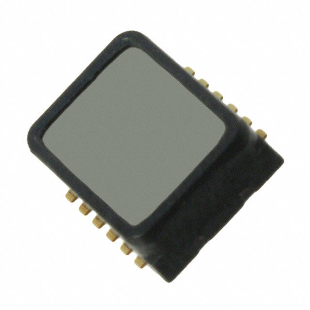
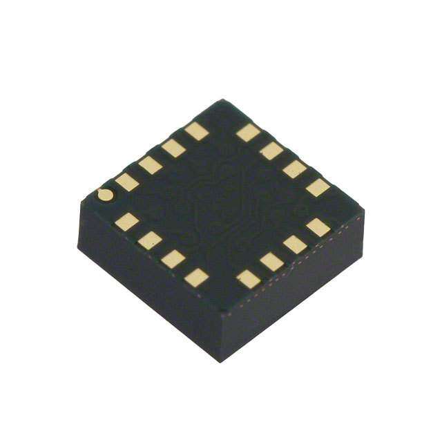
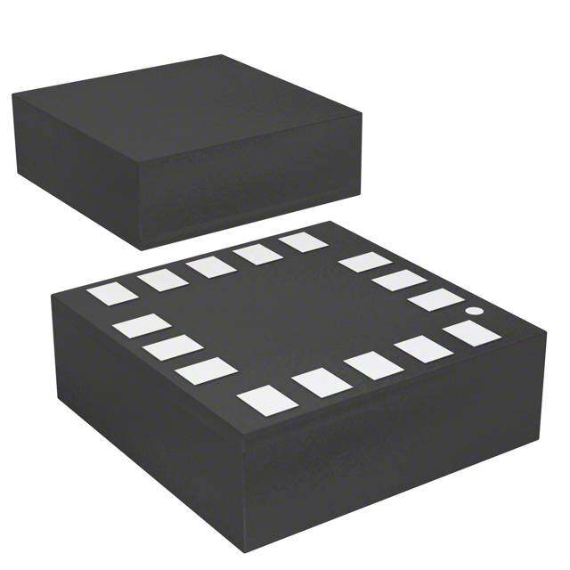
| 描述 | SENSOR ACCEL +/-100/50G 20-SOIC |
| 产品分类 | 加速计 |
| 品牌 | Freescale Semiconductor |
| 数据手册 | |
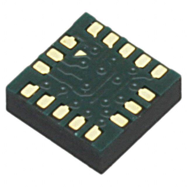
| 产品图片 |
|
| 产品型号 | MMA3202KEGR2 |
| rohs | 无铅 / 符合限制有害物质指令(RoHS)规范要求 |
| 产品系列 | MMA3202 |
| 供应商器件封装 | 20-SOIC W |
| 其它名称 | MMA3202KEGR2DKR |
| 加速度范围 | ±112.5g, 56.3g |
| 安装类型 | 表面贴装 |
| 封装/外壳 | 20-SOIC(0.295",7.50mm 宽) |
| 带宽 | 400Hz |
| 接口 | - |
| 标准包装 | 1 |
| 灵敏度 | 20mV/g,40mV/g |
| 电压-电源 | 4.75 V ~ 5.25 V |
| 轴 | X,Y |
| 输出类型 | 模拟 |


- 商务部:美国ITC正式对集成电路等产品启动337调查
- 曝三星4nm工艺存在良率问题 高通将骁龙8 Gen1或转产台积电
- 太阳诱电将投资9.5亿元在常州建新厂生产MLCC 预计2023年完工
- 英特尔发布欧洲新工厂建设计划 深化IDM 2.0 战略
- 台积电先进制程称霸业界 有大客户加持明年业绩稳了
- 达到5530亿美元!SIA预计今年全球半导体销售额将创下新高
- 英特尔拟将自动驾驶子公司Mobileye上市 估值或超500亿美元
- 三星加码芯片和SET,合并消费电子和移动部门,撤换高东真等 CEO
- 三星电子宣布重大人事变动 还合并消费电子和移动部门
- 海关总署:前11个月进口集成电路产品价值2.52万亿元 增长14.8%

PDF Datasheet 数据手册内容提取
Freescale Semiconductor Document Number: MMA3202KEG Data Sheet: Technical Data Rev 1, 11/2012 Surface Mount Micromachined Accelerometer MMA3202KEG The MMA3202 series of dual axis (X and Y) silicon capacitive, micromachined accelerometers features signal conditioning, a 4-pole low pass filter and temperature compensation and separate outputs for the two axes. Zero-g offset full scale span and filter cut-off are factory set and require no external devices. A MMA3202KEG: X-Y AXIS SENSITIVITY full system self-test capability verifies system functionality. MICROMACHINED ACCELEROMETER Features ±100/50g • Sensitivity in two separate axes: 100g X-axis and 50g Y-axis • Integral Signal Conditioning • Linear Output • Ratiometric Performance • 4th Order Bessel Filter Preserves Pulse Shape Integrity • Calibrated Self-test • Low Voltage Detect, Clock Monitor, and EPROM Parity Check Status • Transducer Hermetically Sealed at Wafer Level for Superior Reliability KEG SUFFIX (Pb-FREE) • Robust Design, High Shocks Survivability 20-LEAD SOIC CASE 475A-02 • Qualified AEC-100, Ref. F Grade 2 (-40°C/+105°C) Typical Applications • Vibration Monitoring and Recording • Impact Monitoring • Appliance Control • Mechanical Bearing Monitoring • Computer Hard Drive Protection • Computer Mouse and Joysticks • Virtual Reality Input Devices • Sports Diagnostic Devices and Systems ORDERING INFORMATION Device Temperature Range Case No. Package MMA3202EG – 40 to +125°C 475A-02 SOIC-20 MMA3202EGR2 – 40 to +125°C 475A-02 SOIC-20, Tape & Reel MMA3202KEG* – 40 to +125°C 475A-02 SOIC-20 MMA3202KEGR2* – 40 to +125°C 475A-02 SOIC-20, Tape & Reel *Part number sourced from a different facility AVDD VDD N/C 1 20 GND G-Cell Integrator Gain Filter Temp XOUT N/C 2 19 N/C Sensor Y N/C 3 18 N/C OUT N/C 4 17 N/C ST 5 16 N/C ST Control Logic & Self-Test EPROM Oscillator Clock XOUT 6 15 N/C Trim Circuits Generator V STATUS 7 14 N/C SS VSS 8 13 N/C VDD 9 12 N/C Status AVDD 10 11 YOUT Figure1. Simplified Accelerometer Functional Block Diagram Figure2. Pin Connections © 2007, 2012 Freescale Semiconductor, Inc. All rights reserved.
Table1. Maximum Ratings (Maximum ratings are the limits to which the device can be exposed without causing permanent damage.) Rating Symbol Value Unit Powered Acceleration (all axes) G 1500 g pd Unpowered Acceleration (all axes) G 2000 g upd Supply Voltage V –0.3 to +7.0 V DD Drop Test (1) D 1.2 m drop Storage Temperature Range T –40 to +125 °C stg 1. Dropped onto concrete surface from any axis. ELECTRO STATIC DISCHARGE (ESD) WARNING: This device is sensitive to electrostatic discharge. Although the accelerometers contain internal 2kV ESD performance or cause failure of the chip. When handling the protection circuitry, extra precaution must be taken by the accelerometer, proper ESD precautions should be followed user to protect the chip from ESD. A charge of over 2000 volts to avoid exposing the device to discharges which may be can accumulate on the human body or associated test detrimental to its performance. equipment. A charge of this magnitude can alter the MMA3202KEG Sensors 2 Freescale Semiconductor, Inc.
Table2. Operating Characteristics (Unless otherwise noted: –40°C T +105°C, 4.75 V 5.25, Acceleration = 0g, Loaded output.)(1) A DD Characteristic Symbol Min Typ Max Unit Operating Range(2) Supply Voltage(3) V 4.75 5.00 5.25 V DD Supply Current I 6 8 10 mA DD Operating Temperature Range T –40 — +125 °C A Acceleration Range X-axis g — 112.5 — g FS Acceleration Range Y-axis g — 56.3 — g FS Output Signal Zero g (T = 25°C, V = 5.0 V)(4) V 2.35 2.5 2.65 V A DD OFF Zero g V 0.46 V 0.50 V 0.54 V V OFF,V DD DD DD Sensitivity X-axis (T = 25°C, V = 5.0 V)(5) S 19 20 21 mV/g A DD Sensitivity Y-axis (T = 25°C, V = 5.0 V) S 38 40 42 mV/g A DD Sensitivity X-axis S 3.72 4 4.28 mV/g/V V Sensitivity Y-axis S 7.44 8 8.56 mV/g/V V Bandwidth Response f 360 400 440 Hz –3dB Nonlinearity NL –1.0 — +1.0 % FSO OUT Noise RMS (.01 Hz – 1 kHz) n — — 2.8 mVrms RMS Power Spectral Density n — 110 — V/(Hz1/2) PSD Clock Noise (without RC load on output)(6) n — 2.0 — mVpk CLK Self-Test Output Response(7) g 9.6 12 14.4 g ST Input Low V V — 0.3 V V IL SS DD Input High V 0.7 V — V V IH DD DD Input Loading(8) I –30 –100 –300 A IN Response Time(9) t — 2.0 – ms ST Status(10) (11) Output Low (I = 100 A) V — — 0.4 V load OL Output High (I = 100 A) V V –0.8 — — V load OH DD Minimum Supply Voltage (LVD Trip) V 2.7 3.25 4.0 V LVD Clock Monitor Fail Detection Frequency f 50 — 260 kHz min Output Stage Performance Electrical Saturation Recovery Time(12) t — 0.2 — ms DELAY Full Scale Output Range (I = 200 A) V 0.25 — V –0.25 V OUT FSO DD Capacitive Load Drive(13) C — — 100 pF L Output Impedence Z — 300 — O Mechanical Characteristics Transverse Sensitivity(14) V — — 5.0 % FSO XZ,YZ Package Resonance f — 10 — kHz PKG 1. For a loaded output the measurements are observed after an RC filter consisting of a 1 k resistor and a 0.01 F capacitor to ground. 2. These limits define the range of operation for which the part will meet specification. 3. Within the supply range of 4.75 and 5.25 volts, the device operates as a fully calibrated linear accelerometer. Beyond these supply limits the device may operate as a linear device but is not guaranteed to be in calibration. 4. The device can measure both + and – acceleration. With no input acceleration the output is at midsupply. For positive acceleration the output will increase above V /2 and for negative acceleration the output will decrease below V /2. DD DD 5. The device is calibrated at 20g. 6. At clock frequency 70 kHz. 7. V calculated with typical sensitivity. OFF 8. The digital input pin has an internal pull-down current source to prevent inadvertent self test initiation due to external board level leakages. 9. Time for the output to reach 90% of its final value after a self-test is initiated. 10. The Status pin output is not valid following power-up until at least one rising edge has been applied to the self-test pin. The Status pin is high whenever the self-test input is high, as a means to check the connectivity of the self-test and Status pins in the application. 11. The Status pin output latches high if a Low Voltage Detection or Clock Frequency failure occurs, or the EPROM parity changes to odd. The Status pin can be reset low if the self-test pin is pulsed with a high input for at least 100 s, unless a fault condition continues to exist. 12. Time for amplifiers to recover after an acceleration signal causing them to saturate 13. Preserves phase margin (60°) to guarantee output amplifier stability. 14. A measure of the device's ability to reject an acceleration applied 90° from the true axis of sensitivity. MMA3202KEG Sensors Freescale Semiconductor, Inc. 3
PRINCIPLE OF OPERATION The Freescale accelerometer is a surface-micromachined between the plates. The X-Y device contains two structures integrated-circuit accelerometer. at right angles to each other. The device consists of a surface micromachined The CMOS ASIC uses switched capacitor techniques to capacitive sensing cell (g-cell) and a CMOS signal measure the g-cell capacitors and extract the acceleration conditioning ASIC contained in a single integrated circuit data from the difference between the two capacitors. The package. The sensing element is sealed hermetically at the ASIC also signal conditions and filters (switched capacitor) wafer level using a bulk micromachined “cap'' wafer. the signal, providing a high level output voltage that is The g-cell is a mechanical structure formed from ratiometric and proportional to acceleration. semiconductor materials (polysilicon) using semiconductor processes (masking and etching). It can be modeled as two stationary plates with a moveable plate in-between. The Acceleration center plate can be deflected from its rest position by subjecting the system to an acceleration (Figure3). When the center plate deflects, the distance from it to one fixed plate will increase by the same amount that the distance to the other plate decreases. The change in distance is a measure of acceleration. The g-cell plates form two back-to-back capacitors (Figure4). As the center plate moves with acceleration, the Figure3.Transducer Figure4.Equivalent distance between the plates changes and each capacitor's Physical Model Circuit Model value will change, (C = A/D). Where A is the area of the plate, is the dielectric constant, and D is the distance SPECIAL FEATURES Filtering plate and the moveable plate. The resulting electrostatic The Freescale accelerometers contain an onboard 2-pole 1 V2 switched capacitor filter. A Bessel implementation is used force Fe= 2---A-d---2--causes the center plate to deflect. because it provides a maximally flat delay response (linear phase) thus preserving pulse shape integrity. Because the The resultant deflection is measured by the accelerometer's filter is realized using switched capacitor techniques, there is control ASIC and a proportional output voltage results. This no requirement for external passive components (resistors procedure assures that both the mechanical (g-cell) and and capacitors) to set the cut-off frequency. electronic sections of the accelerometer are functioning. Self-Test Status The sensor provides a self-test feature that allows the Freescale accelerometers include fault detection circuitry verification of the mechanical and electrical integrity of the and a fault latch. The Status pin is an output from the fault accelerometer at any time before or after installation. This latch, OR'd with self-test, and is set high whenever the feature is critical in applications such as automotive airbag following event occurs: systems where system integrity must be ensured over the life • Parity of the EPROM bits becomes odd in number. of the vehicle. A fourth “plate'' is used in the g-cell as a self- The fault latch can be reset by a rising edge on the self-test test plate. When the user applies a logic high input to the self- input pin, unless one (or more) of the fault conditions test pin, a calibrated potential is applied across the self-test continues to exist. MMA3202KEG Sensors 4 Freescale Semiconductor, Inc.
BASIC CONNECTIONS PINOUT DESCRIPTION PCB Layout STATUS P1 N/C 1 20 GND ST P0 N/C 2 19 N/C er M et X R A/D In ic N/C 3 18 N/C m OUT ro NS/CT 54 1167 NN//CC Accelero YOUT 1 Rk C 0.01 F A/D In controlle VSS C 0.1 F XOUT 6 15 N/C VSS 1 k C 0.01 F r VDD STATUS 7 14 N/C C 0.1 F V VSS 8 13 N/C DD V RH VDD 9 12 N/C C 0.1 F AVDD 10 11 YOUT Power Supply Table3. Pin Descriptions Pin No. Pin Name Description Figure5. Recommended PCB Layout for Interfacing Accelerometer to Microcontroller 1 thru 3 — Leave unconnected. NOTE: 4 — No internal connection. Leave • Use a 0.1 F capacitor on V to decouple the power DD unconnected. source. 5 ST Logic input pin used to initiate self-test. • Physical coupling distance of the accelerometer to the microcontroller should be minimal. 6 X Output voltage of the accelerometer. X OUT • Place a ground plane beneath the accelerometer to Direction. reduce noise, the ground plane should be attached to all 7 STATUS Logic output pin to indicate fault. of the open ended terminals shown in Figure5. • Use an RC filter of 1 k and 0.01 F on the output of the 8 V The power supply ground. SS accelerometer to minimize clock noise (from the switched 9 VDD The power supply input. capacitor filter circuit). • PCB layout of power and ground should not couple power 10 AV Power supply input (Analog). DD supply noise. 11 Y Output voltage of the accelerometer. Y OUT • Accelerometer and microcontroller should not be a high Direction. current path. 12 thru 16 — Used for factory trim. Leave • A/D sampling rate and any external power supply unconnected. switching frequency should be selected such that they do not interfere with the internal accelerometer sampling 17 thru 19 — No internal connection. Leave frequency. This will prevent aliasing errors. unconnected. 20 GND Ground. 7 V MMA3202EG Status DD Logic 5 ST R1 Input 9 VDD XOUT 6 1 k X Output Signal C1 10 AV 0.1 F DD C2 8 VSS 0.01 F R2 Y 11 1 k Y Output OUT Signal C3 0.01 F Figure4. SOIC Accelerometer with Recommended Connection Diagram MMA3202KEG Sensors Freescale Semiconductor, Inc. 5
Dynamic Acceleration Sensing Direction Y N/C 1 20 GND N/C 2 19 N/C N/C 3 18 N/C Acceleration of the package in the X and Y direction N/C 4 17 N/C Activation of Self test moves the (center plates move in the X ST 5 16 N/C X center plates in the X and Y X and Y direction) will result in XOUT 6 15 N/C direction, resulting in an increase an increase in the X and Y in the X and Y outputs. STATUS 7 14 N/C outputs. VSS 8 13 N/C VDD 9 12 N/C AVDD 10 11 YOUT Y 20-Pin SOIC Package N/C pins are recommended to be left FLOATING Top View Static Acceleration Sensing Direction 10 9 8 7 6 5 4 3 2 1 Direction of Earth’s gravity field.* 11 12 13 14 15 16 17 18 19 20 Front View Side View * When positioned as shown, the Earth’s gravity will result in a positive 1g output in the X channel. MMA3202KEG Sensors 6 Freescale Semiconductor, Inc.
MINIMUM RECOMMENDED FOOTPRINT FOR SURFACE MOUNTED APPLICATIONS Surface mount board layout is a critical portion of the total footprint, the packages will self-align when subjected to a design. The footprint for the surface mount packages must be solder reflow process. It is always recommended to design the correct size to ensure proper solder connection interface boards with a solder mask layer to avoid bridging and between the board and the package. With the correct shorting between solder pads. 0.050 in. 0.380 in. 1.27 mm 9.65 mm 0.024 in. 0.610 mm 0.080 in. 2.03 mm Figure6. Footprint SOIC-20 (Case 475A-02) MMA3202KEG Sensors Freescale Semiconductor, Inc. 7
PACKAGE DIMENSIONS PAGE 1 OF 2 CASE 475A-02 ISSUE C 20-LEAD SOIC MMA3202KEG Sensors 8 Freescale Semiconductor, Inc.
PACKAGE DIMENSIONS PAGE 2 OF 2 CASE 475A-02 ISSUE C 20-LEAD SOIC MMA3202KEG Sensors Freescale Semiconductor, Inc. 9
Table 4. Revision History Revision Revision Description of changes number date 1 11/2012 • Table 2. Operating Characteristics, added footnote for Self-Test Output Response, updated page 4: Principle of Operation MMA3202KEG Sensors Freescale Semiconductor, Inc. 10
How to Reach Us: Information in this document is provided solely to enable system and software implementers to use Freescale products. There are no express or implied copyright Home Page: licenses granted hereunder to design or fabricate any integrated circuits based on the freescale.com information in this document. Web Support: freescale.com/support Freescale reserves the right to make changes without further notice to any products herein. Freescale makes no warranty, representation, or guarantee regarding the suitability of its products for any particular purpose, nor does Freescale assume any liability arising out of the application or use of any product or circuit, and specifically disclaims any and all liability, including without limitation consequential or incidental damages. “Typical” parameters that may be provided in Freescale data sheets and/or specifications can and do vary in different applications, and actual performance may vary over time. All operating parameters, including “typicals,” must be validated for each customer application by customer’s technical experts. Freescale does not convey any license under its patent rights nor the rights of others. Freescale sells products pursuant to standard terms and conditions of sale, which can be found at the following address: freescale.com/salestermsandconditions. Freescale, the Freescale logo, Energy Efficient Solutions logo, are trademarks of Freescale Semiconductor, Inc., Reg. U.S. Pat. & Tm. Off. Xtrinsic is a trademark of Freescale Semiconductor, Inc. All other product or service names are the property of their respective owners. © 2012 Freescale Semiconductor, Inc. MMA3202KEG Rev. 1 11/2012