ICGOO在线商城 > 传感器,变送器 > 运动传感器 - 加速计 > FXLC95000CLR1
 Datasheet下载
- 型号: FXLC95000CLR1
- 制造商: Freescale Semiconductor
- 库位|库存: xxxx|xxxx
- 要求:
| 数量阶梯 | 香港交货 | 国内含税 |
| +xxxx | $xxxx | ¥xxxx |
查看当月历史价格
查看今年历史价格
FXLC95000CLR1产品简介:
ICGOO电子元器件商城为您提供FXLC95000CLR1由Freescale Semiconductor设计生产,在icgoo商城现货销售,并且可以通过原厂、代理商等渠道进行代购。 FXLC95000CLR1价格参考。Freescale SemiconductorFXLC95000CLR1封装/规格:运动传感器 - 加速计, Accelerometer X, Y, Z Axis ±2g, 4g, 8g 24-LLP-EP (4x5)。您可以下载FXLC95000CLR1参考资料、Datasheet数据手册功能说明书,资料中有FXLC95000CLR1 详细功能的应用电路图电压和使用方法及教程。
FXLC95000CLR1 是由 NXP USA Inc. 推出的一款高性能、低功耗的三轴数字加速度传感器,属于运动传感器中的加速计类别。该器件基于 MEMS 技术,具备高精度和出色的稳定性,适用于对空间占用和能耗要求严苛的应用场景。

其主要应用场景包括:便携式消费类电子产品(如智能手机、平板电脑、可穿戴设备)中的屏幕自动旋转、步数计数和手势识别;工业自动化领域中用于设备状态监测、振动检测和倾斜测量;在物联网(IoT)终端设备中实现运动唤醒和节能管理;还可用于智能家居设备(如智能门铃、安防摄像头)中的移动侦测功能,提升系统响应效率与安全性。

此外,FXLC95000CLR1 因其小型封装和高抗冲击能力,也适合应用于汽车电子中的非安全相关监测系统,如车载信息娱乐系统的运动感应或黑匣子中的行驶状态记录。整体而言,该传感器广泛服务于需要精准感知动态加速度变化的智能化系统,尤其适合注重低功耗与高集成度的设计需求。
| 参数 | 数值 |
| 产品目录 | |
| 描述 | MOTION SENSOR 3-AXIS CF V1 24LGA板机接口移动感应器和位置传感器 3-axis, Coldfire v1 core |
| 产品分类 | 加速计运动与定位传感器 |
| 品牌 | Freescale Semiconductor |
| 产品手册 | |
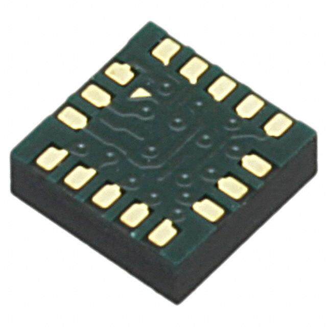
| 产品图片 |
|
| rohs | RoHS 合规性豁免无铅 / 符合限制有害物质指令(RoHS)规范要求 |
| 产品系列 | 板机接口移动感应器和位置传感器,Freescale Semiconductor FXLC95000CLR1- |
| 数据手册 | |
| 产品型号 | FXLC95000CLR1 |
| 产品种类 | 板机接口移动感应器和位置传感器 |
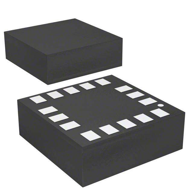
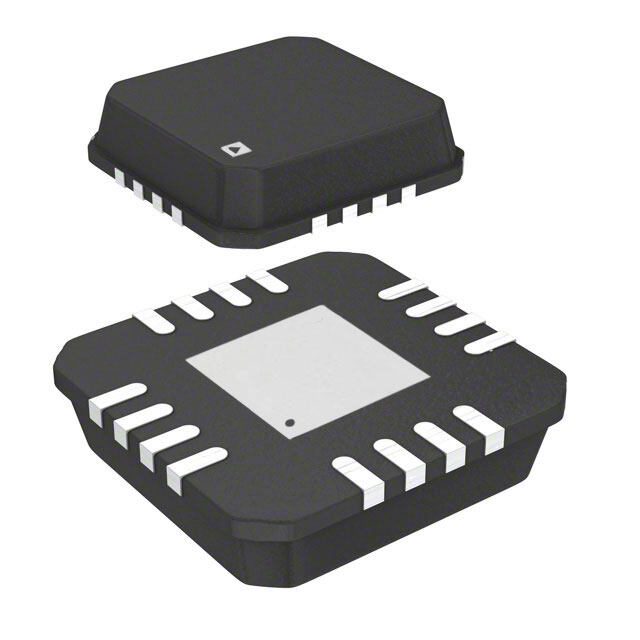
| 供应商器件封装 | 24-LLP-EP(4x5) |
| 其它名称 | FXLC95000CLR1DKR |
| 加速度范围 | ± 2g, 4g, 8g |
| 单位重量 | 33.800 mg |
| 商标 | Freescale Semiconductor |
| 安装类型 | 表面贴装 |
| 安装风格 | SMD/SMT |
| 封装 | Reel |
| 封装/外壳 | 24-TFLGA |
| 封装/箱体 | LGA-24 |
| 工厂包装数量 | 1000 |
| 带宽 | - |
| 接口 | I²C, SPI |
| 数字输出-位数 | 16 bit |
| 最大工作温度 | + 85 C |
| 最小工作温度 | - 40 C |
| 标准包装 | 1 |
| 灵敏度 | 0.061mg/LSB,0.122mg/LSB,0.244mg/LSB |
| 特点 | 3 Axis MEMS accelerometer and 32 bit ColdFire MCU |
| 电压-电源 | 1.71 V ~ 1.89 V |
| 电源电压-最大 | 3.6 V |
| 电源电压-最小 | 1.71 V |
| 轴 | X,Y,Z |
| 输出类型 | I²C, SPI |
| 配用 | /product-detail/zh/KITFXLC95000MAG/KITFXLC95000MAG-ND/4579633 |


- 商务部:美国ITC正式对集成电路等产品启动337调查
- 曝三星4nm工艺存在良率问题 高通将骁龙8 Gen1或转产台积电
- 太阳诱电将投资9.5亿元在常州建新厂生产MLCC 预计2023年完工
- 英特尔发布欧洲新工厂建设计划 深化IDM 2.0 战略
- 台积电先进制程称霸业界 有大客户加持明年业绩稳了
- 达到5530亿美元!SIA预计今年全球半导体销售额将创下新高
- 英特尔拟将自动驾驶子公司Mobileye上市 估值或超500亿美元
- 三星加码芯片和SET,合并消费电子和移动部门,撤换高东真等 CEO
- 三星电子宣布重大人事变动 还合并消费电子和移动部门
- 海关总署:前11个月进口集成电路产品价值2.52万亿元 增长14.8%


PDF Datasheet 数据手册内容提取
Freescale Semiconductor, Inc. FXLC95000CL Data Sheet: Technical Data Rev 1.2, 8/2013 Xtrinsic FXLC95000CL Intelligent, FXLC95000CL Motion-Sensing Platform The FXLC95000CL Intelligent, Motion-Sensing Platform is a breakthrough device with the integration of a 3-axis MEMS accelerometer and a 32-bit ColdFire MCU that enables autonomous, high-precision sensing solutions with local computing and sensors management capability in an open, easy to use, architecture. The FXLC95000CL hardware is user-programmable to create an 24-LEAD LGA 3 mm by 5 mm by 1 mm intelligent high-precision, flexible, motion-sensing platform. The Case 2208-01 user's firmware, together with the hardware device, can make system-level decisions required for sophisticated applications, such as gesture recognition, pedometer, and e-compass tilt compensation and calibration. Top View Taonrh deS PaFI X hmLigCohd9lyu5 l0ceo0, n0thf ipegl uaFrtXfaobLrlmCe9 dc5ea0cn0i s0ai coptn laa etsfn oagrnmin i enc.ta eUnlls imgineagnn tta hsgeee nM ssaienscgtoe hnr udI2baCry O8 / PDB_B O13 / SSB1 O12 / MISO1 sensors such as pressure sensors, magnetometers, and VSSA RGPI VDDA RGPI RGPI gyroscopes. The embedded microcontroller allows sensor RGPIO14 / SCL1 RGPIO11 / MOSI1 integration, initialization, calibration, data compensation, and RGPIO15 / SDA1 RGPIO10 / SCLK1 computation functions to be added to the platform, thereby off- VSSIO RGPIO7 / AN1+ / TPMCH1 loading those functions from the host processor. Total system VDDIO RGPIO6 / AN0- / TPMCH0 VDD RGPIO5 / PDB_A / INT_O power consumption is significantly reduced because the BKGD-MS / RGPIO9 VSS application processor stays powered down for longer periods of RESETB RGPIO4 / INT_I time. TCIeDnhoEaed)b e.Fl WeTXshLa icCrsru i9sos5trtao 0Dnm0de0eavCrersdLl o, t dopine mqtveueicgincertka iSltsyet updimdr doipoegl evrfaomemrloe Mmpnmtiec cdreuo nascttno oednmn tcrv ooeirlnmolefnirbgm e(uEdercednldeti p d(wsIDeitEh) SCL0 / RGPIO0 / SCLK VSS SDA0 / RGPIO1 / MOSI RGPIO2 / SCL1 / MISO RGPIO3 / SDA1 / SSB algorithms and features to exactly match their application needs. Pin Connections Hardware Features • 3-axis low noise accelerometer • ±2 g, ±4 g, ±8 g configurable dynamic ranges available • Up to 16-bit resolution • 32-bit MCU • Coldfire V1 CPU with MAC hardware unit • 128K Flash, 16K RAM, 16K ROM • 10-, 12-, 14-, and 16-bit, trimmed analog-to-digital converter (ADC) data formats available • Master and slave, I2C and SPI serial connectivity modules • Sleep and low power modes to enable local power Freescale reserves the right to change the detail specifications as may be required to permit improvements in the design of its products. © 2012–2013 Freescale Semiconductor, Inc. All rights reserved.
• Wide operating voltage and temperature range • 1.71 to 3.6 V I/O supply voltage • –40ºC to +85ºC operating temperature range • Small package footprint • 3 mm x 5 mm x 1 mm 24-pin LGA package Ordering Information Part number Temperature range Package description Shipping FXLC95000CLR1 –40°C to +85°C LGA-24 Tape and reel 2 Xtrinsic FXLC95000CL Intelligent, Motion-Sensing Platform, Rev1.2, 8/2013. Freescale Semiconductor, Inc.
Table of Contents 1 Typical Applications..............................................................4 5.2 Absolute maximum ratings..........................................21 2 Software Support..................................................................4 5.3 Operating conditions....................................................22 3 Related Documentation.........................................................5 5.4 General DC characteristics..........................................23 4 General Description..............................................................5 5.5 Supply current characteristics......................................23 4.1 Functional overview.....................................................5 5.6 Accelerometer transducer mechanical characteristics24 4.1.1 ROM content and usage..................................7 5.7 Temperature sensor characteristics............................25 4.2 Pinout...........................................................................7 5.8 ADC characteristics.....................................................25 4.2.1 Pin function description....................................9 5.9 AC electrical characteristics.........................................26 4.3 System connections.....................................................12 5.10 General timing control..................................................27 4.3.1 Power supply considerations...........................12 5.11 Interfaces.....................................................................28 4.3.2 General connections and layout 5.12 Flash parameters.........................................................31 recommendations............................................13 6 Package Information.............................................................32 4.3.3 I2C reset considerations..................................14 6.1 Product Identification Markings....................................32 4.3.4 FXLC95000CL as an intelligent slave..............14 6.2 Footprint and pattern information.................................32 4.3.5 FXLC95000CL as a sensor hub......................16 6.3 Tape and reel information............................................35 4.4 Sensing direction and output response.......................19 6.4 Package dimensions....................................................35 5 Mechanical and Electrical Specifications..............................20 7 Revision History....................................................................37 5.1 Definitions....................................................................21 Xtrinsic FXLC95000CL Intelligent, Motion-Sensing Platform, Rev1.2, 8/2013. 3 Freescale Semiconductor, Inc.
Typical Applications 1 Typical Applications This low-power intelligent sensor platform is optimized for a variety of applications. • Mobile phones/PMP/PDA/Digital cameras • E-Compass applications with tilt compensation • Smartbooks/e-readers/netbooks/laptops • Pedometers • Gaming and toys • Virtual-reality, 3D position feedback • Personal navigation devices (PNDs) • Activity monitoring in medical and fitness applications • Security • Fleet monitoring and tracking • Power tools and small appliances 2 Software Support The Xtrinsic Intelligent Sensing Framework (ISF) is a software framework built on top of Freescale’s MQX real time operating system (RTOS). ISF offers an open programming model with library support for FXLC95000CL devices. The flexibility of this open programming model allows the FXLC95000CL to be delivered ready to accept a customer’s choice of firmware images. A number of pre-built firmware images are available for download from the Freescale website, or, using CodeWarrior and ISF, a customer may create their own custom firmware image incorporating sensor processing algorithms of their own design. Sensor Adapter libraries for a number of additional Freescale sensors are also available for download enabling the FXLC95000CL to become a sensor hub. 4 Xtrinsic FXLC95000CL Intelligent, Motion-Sensing Platform, Rev1.2, 8/2013. Freescale Semiconductor, Inc.
Related Documentation 3 Related Documentation The FXLC95000CL device's features and operations are described in a variety of reference manuals, user guides, and application notes. To find the most-current versions of these documents: 1. Go to the Freescale homepage at freescale.com. 2. In the Keyword search box at the top of the page, enter the device number FXLC95000CL. 3. In the Refine Your Result pane on the left, click on the Documentation link. 4 General Description 4.1 Functional overview The FXLC95000CL platform consists of a three-axis, MEMS accelerometer and a mixed-signal ASIC with an integrated, 32-bit CPU. The mixed-signal ASIC can be utilized to measure and condition the outputs of the MEMS accelerometer, internal temperature sensor, or a differential analog signal from an external device. These measured values can be read at different sample rates through a subscription mechanism in the Intelligent Sensing Framework (ISF) and/or utilized internally by firmware for the FXLC95000CL device (Freescale supplied or user-written). Xtrinsic FXLC95000CL Intelligent, Motion-Sensing Platform, Rev1.2, 8/2013. 5 Freescale Semiconductor, Inc.
General Description INT_I BKGD/MS Interrupt 16 KB controller ColdFire ROM V1 CPU 128 KB 16 KB Flash RAM memory Analog Front End 16 Flash controller Temperature sensor 8 I2C master / SDA1,SCL1 3-axis Drive circuit ADC Peripheral 16 accelerometer bus interface 16 SPI master / MOSI, MISO, SCLK2. SSB2 transducer C2V Trim 8 2 x 8 Port control 8 16-bit modulo System Integration timer RESETB Module SSCSLBK SPI slave 16 PrDoeglraaym Bmloacbkle / PPDDBB__AB, MOSI MISO Control and 8 8 Two-channel / TPMCH0, mailbox TPM TPMCH1 register set 8 SDA0 I2C slave 8 Clock module SCL0 (16 MHz) SP_SCR[PS] Eclxotecrknal Icnlotecrknal 16 RGPIO[15:0] / RRGGPPIIOO01,5 ... , domain domain Figure 1. Block diagram of the FXLC95000CL A block level view of the FXLC95000CL platform is shown in Figure 1 and can be summarized at a high level as an analog/mixed mode subsystem associated with a digital engine. The analog sub-system is composed of: • A 3-axis MEMS transducer • An Analog Front End (AFE) with: • A capacitance-to-voltage converter • An analog-to-digital converter • A temperature sensor The digital sub-system is composed of: • A 32-bit, ColdFire V1 CPU with Background Debug Module (BDM) • Memory: RAM, ROM, and flash • Rapid General Purpose Input/Output (RGPIO) port control logic • Timer functions: • Modulo Timer Module (MTIM16) • Programmable Delay Timer (PDB) • General-Purpose Timer/Pulse-Width Modulation Module (TPM) 6 Xtrinsic FXLC95000CL Intelligent, Motion-Sensing Platform, Rev1.2, 8/2013. Freescale Semiconductor, Inc.
General Description • I2C master interface • Queued SPI master interface (This interface has both send and receive FIFOs of size 16 bit wordlength and 4 words depth each. No DMA.) • I2C or SPI slave interface • System Integration Module (SIM) • Clock-generation module The slave interfaces (either SPI or I2C) operate independently of the ColdFire CPU subsystem. This allows the host processor to access the slave interface at any time, including while the FXLC95000CL's CPU is in low-power, deep-sleep mode. Host access can be set to trigger a FXLC95000CL CPU wakeup. 4.1.1 ROM content and usage There are several classes of functions stored in ROM: • A Boot program, including ROM-based slave port command interpreter. • A collection of utilities which can be invoked via the ROM-based slave port command interpreter. • ROM functions which are callable from user code using the call_trap() function. For a detailed description of these items, refer to the FXLC95000CL Hardware Reference Manual ROM chapter. The FXLC95000CL device boots from a standard routine in ROM. This boot function is responsible for a number of initialization steps (in particular the state of GPIO8 pin is checked in order to select either I2C or SPI interface as serial communication Slave port), before transferring control if desired to user code in flash memory (when the Boot from Flash bit-field has been set). The ROM contains a simple command interpreter capable of running a number of ROM-based utility and test functions. These ROM-based functions support flash memory programming and erasing, the protection of flash, the device Reset, and the reading of device information. They also provide useful error codes. The FXLC95000CL platform is supplied with a fully erased flash memory. Users can take advantage of the ROM-based flash controller and slave port command-line interpreter to communicate with a virgin device and program custom firmware into the flash array. Xtrinsic FXLC95000CL Intelligent, Motion-Sensing Platform, Rev1.2, 8/2013. 7 Freescale Semiconductor, Inc.
General Description 4.2 Pinout B 1 O1 DB_ SSB MIS 8 / P 13 / 12 / O O O VSSA RGPI VDDA RGPI RGPI RGPIO14 / SCL1 RGPIO11 / MOSI1 RGPIO15 / SDA1 RGPIO10 / SCLK1 VSSIO RGPIO7 / AN1+ / TPMCH1 VDDIO RGPIO6 / AN0- / TPMCH0 VDD RGPIO5 / PDB_A / INT_O BKGD-MS / RGPIO9 VSS RESETB RGPIO4 / INT_I SCL0 / RGPIO0 / SCLK VSS SDA0 / RGPIO1 / MOSI RGPIO2 / SCL1 / MISO RGPIO3 / SDA1 / SSB Figure 2. Device pinout (top view) Table 1. Pin functions Pin # Default Pin Pin Function Pin Function Description Function1 #2 #3 1 SCL12 RGPIO14 Master I2C Clock / RGPIO14 2 SDA13 RGPIO15 Master I2C Data / RGPIO15 3 V I/O ground SSIO 4 V I/O power supply DDIO 5 V Digital power supply DD 6 BKGD/MS RGPIO9 Background debug - Mode select / RGPIO9 7 RESETB4 Active low reset with internal, pullup resistor 8 SCL0 RGPIO0 SCLK Serial clock for slave I2C / RGPIO0 / Serial clock for slave SPI 9 V Digital ground SS 10 SDA0 RGPIO1 MOSI Serial data for slave I2C / RGPIO1 / SPI Master Output Slave Input 11 RGPIO2 SCL1 MISO RGPIO2 / Serial clock for master I2C / SPI Master Input Slave Output 12 RGPIO3 SDA1 SSB RGPIO3 / Serial data for master I2C / SPI slave select 13 RGPIO4 INT_I RGPIO4 / Interrupt input 14 V Must be connected to GND externally SS 15 RGPIO5 PDB_A INT_O RGPIO5 / PDB_A / Interrupt output Table continues on the next page... 8 Xtrinsic FXLC95000CL Intelligent, Motion-Sensing Platform, Rev1.2, 8/2013. Freescale Semiconductor, Inc.
General Description Table 1. Pin functions (continued) Pin # Default Pin Pin Function Pin Function Description Function1 #2 #3 16 RGPIO6 AN0- TPMCH0 RGPIO6 / ADC Input 0 / TPM Channel 0 17 RGPIO7 AN1+ TPMCH1 RGPIO7 / ADC Input 1 / TPM Channel 1 18 SCLK1 RGPIO10 master queued SPI clock / RGPIO10 19 MOSI1 RGPIO11 master queued SPI Master Output Slave Input / RGPIO11 20 MISO1 RGPIO12 master queued SPI Master Input Slave Output / RGPIO12 21 SSB1 RGPIO13 master queued SPI slave select / RGPIO13 22 V Analog power DDA 235 RGPIO8 PDB_B RGPIO8 / PDB_B 24 V Analog ground SSA 1. Default Pin Function 1 represents the reset state of the device. Pin functions may be changed via the SIM pin mux- control registers. Drive strength and pullup controls are programmed by the port control registers. 2. SCL1 is available for use on pin (RGPIO14) only when SIM_PMCR1[A2] is not equal to "01". That setting would enable it for pin 11 (RGPIO2). 3. SDA1 is available for use on pin (RGPIO15) only when SIM_PMCR1[A3] is not equal to "01". That setting would enable it for pin 12 (RGPIO3). 4. RESETB defaults to input only, but can be configured as an open-drain, bidirectional pin. 5. GPIO8/PDB_B = LOW at startup indicates that SPI should be used as slave instead of the I2C module. 4.2.1 Pin function description Descriptions of the pin functions available on this device are provided in this section. Sixteen of the device pins are multiplexed with Rapid GPIO (RGPIO) functions. The Default Pin Function column of Table 1 lists which function is active when the device exits the reset state. User firmware can use the Pin Mux Control registers in the System Integration Module (SIM) to change pin assignments for these pins after reset. V and V DDIO SSIO I/O power and ground. V ranges from 1.71V to 3.6V for this device. The device DDIO will not load the I2C bus if V is not connected. Parasitic paths to supply this DDIO power domain from other pins is not recommended. V and V DD SS Digital power and ground. V is nominally 1.8V for this device. Parasitic paths to DD supply this power domain from other pins is not recommended. V and V DDA SSA Xtrinsic FXLC95000CL Intelligent, Motion-Sensing Platform, Rev1.2, 8/2013. 9 Freescale Semiconductor, Inc.
General Description Analog power and ground. V is nominally 1.8V for this device. It is recommended DDA that this supply voltage be filtered to remove any digital noise that may be present on the supply. RESETB The RESETB pin is an open-drain, bidirectional pin. At power up, it is configured strictly as an input pin. Setting RCSR[DR] (Reset Control & Status Register “Drive Reset” bit) to one will cause the RESET function to become bidirectional. Using this feature, FXLC95000CL can reset external devices whenever it is reset for any purpose other than power-on-reset. Slave I2C: SDA0, SCL0 Slave I2C data and clock signals. FXLC95000CL may be controlled via this serial port or via the slave SPI interface. At reset, SDA0 and SCL0 are open-drain, bidirectional in input mode, with the pullup resistor disabled. Master I2C: SDA1, SCL1 Master I2C data and clock signals. Because the FXLC95000CL contains a 32-bit ColdFire V1 CPU, it is fully capable of mastering other devices in the system via this serial port. State at reset: active. SCL1 and SDA1 are configured on pins 1 and 2, respectively. The alternate functionality on these pins is RGPIO14 and RGPIO15. Analog-to-Digital Conversion: AN0, AN1 The on-chip ADC can be used to perform a differential analog-to-digital conversion based upon the voltage present across pins AN0(-) and AN1(+). Conversions for these pins are at the same Sample Data Rate (SDR) as the MEMS transducer signals. State at reset: Inactive. AN[1:0] are secondary functions on RGPIO[7:6], which own the pins at reset. Rapid General Purpose I/O: RGPIO[15:0] The ColdFire V1 CPU has a feature called “Rapid GPIO” or RGPIO. This is a 16-bit input/output port with single-cycle write, set, clear, and toggle functions available to the CPU. The FXLC95000CL brings out all 16 bits of that port as pins of the device. State at reset: • RGPIO[15:14]: inactive. SDA1 and SCL1 own the pin at reset. 10 Xtrinsic FXLC95000CL Intelligent, Motion-Sensing Platform, Rev1.2, 8/2013. Freescale Semiconductor, Inc.
General Description • RGPIO[13:10, 8:2]: Pin mux registers for these bits are configured as RGPIO. Pullups are disabled. RGPIO functionality can be enabled via RGPIO_ENB[13:10, 8:2]. • RGPIO[9]: Inactive. BKGD/MS owns the pin at reset • RGPIO[1:0]: inactive. SDA0 and SCL0 own the pin at reset. Configuration details: • RGPIO[15:14] are configured as Master I2C port at reset when RGPIO_ENB[15:14]=00 and PMCR[A3]=PMCR[A2]=00 or 10. They can only be configured as RGPIO when PMCR[A3]=PMCR[A2]=01. RGPIO_ENB[15:14] must also be set to 11 for them to assume RGPIO functionality. • RGPIO_ENB[13:10] are used to configure RGPIO[13:10]. • Pin function selections are made via the SIM pin mux registers for RGPIO[9:0]. Interrupts: INT_I This input pin may be used to wake the CPU from a deep-sleep mode. It can be programmed to trigger on either rising or falling edge or high or low level. This pin operates as a level 7 (high priority) interrupt. Interrupts: INT_O RGPIO5 (pin 11) can be configured to function as an interrupt output pin. This interrupt can be asserted via software when a command response packet has been stored on the slave port mailboxes and is ready for the host to read. The host will see the interrupt and can read the data from the FXLC95000CL platform. The FXLC95000CL will automatically clear the interrupt once it recognizes that the response packet is being transmitted. This clearing action occurs while the packet is being read and prevents the host from falsely recognizing the same interrupt after the packet read is complete. State at reset: Pin muxing is set to RGPIO5 mode. Debug/Mode Control: BKGD/MS At power-up, this pin operates as Mode Select. If low during power-up, the CPU will boot into debug halt mode. If high, the CPU will boot normally and run code. After power-on reset, this pin operates as a bidirectional, single-wire Background Debug port. CodeWarrior uses the Background Debug port to download code into on-chip RAM and flash, and for debugging that code using breakpoints and single stepping. State at reset: Mode Select (MS). MS = 1'b0, at exit from reset → boot to debug halt mode. Xtrinsic FXLC95000CL Intelligent, Motion-Sensing Platform, Rev1.2, 8/2013. 11 Freescale Semiconductor, Inc.
General Description MS = 1'b1, at exit from reset → boot to run mode. State after reset: BKGD. The BKGD pin is a bidirectional, pseudo-open-drain pin used for communications with a debug environment. Programmable Delay Block: PDB_A, PDB_B These are the two outputs of the programmable delay block (PDB). Normally, the PDB is used to schedule internal events at some fixed interval(s) relative to start of either the analog or digital phase. By bringing the PDB outputs to these pins, it becomes possible for the FXLC95000CL to initiate some external event, also relative to start of analog or digital phase. For more information, refer to the FXLC95000CL Hardware Reference Manual. Timer: TPMCH0 and TPMCH1 These pins are the outputs for a general modulo 16 timer and general input/output capture (TPM) and pulse width modulation (PWM) functions. Slave SPI Interface: SCLK, MOSI, MISO, SSB Slave SPI clock, master-output slave-input, master-input slave-output, and slave-select signals. The FXLC95000CL may be controlled via this serial port or via the slave I2C interface. State at reset: In reset, these pins are configured according to I2C and RGPIO[3:2] functions listed above. The pin may be reconfigured for SPI use as part of the boot process. Master SPI Interface: SCLK1, MOSI1, MISO1, SSB1 Master SPI clock, master-output slave-input, master-input slave-output, and slave-select signals. State at reset: In reset, these pins are configured as RGPIO[13:10] functions listed above. 4.3 System connections The FXLC95000CL platform offers the choice of connecting to a host processor through either an I2C or SPI interface. It can also act as a master controller for I2C or SPI peripherals and analog sensors. 12 Xtrinsic FXLC95000CL Intelligent, Motion-Sensing Platform, Rev1.2, 8/2013. Freescale Semiconductor, Inc.
General Description 4.3.1 Power supply considerations • An internal circuit powered by V provides the FXLC95000CL with a power- DDA on-reset signal. For this signal to be properly recognized, it is important that V DD is powered up before or simultaneously with V . DDA • The voltage potential difference between V and V must not exceed ±0.1 V. DD DDA The simplest way to accomplish this is to power both pins from the same voltage source. • When using the same voltage source, some digital noise might reach the analog section. To prevent this, connect a small inductor or ferrite bead in serial with both the V and V traces. Additionally, two ceramic capacitors (of DDA SSA approximately 1 µF, and 100 nF, respectively) can be used to efficiently bypass the power and ground of both digital and analog supply rails. • V must rise up before or simultaneously with V /V . DDIO DDA DD 4.3.2 General connections and layout recommendations • Provide a low-impedance path from the board power supply to each power pin (VDD, VDDA, and VDDIO) on the device and from the board ground to each ground pin (VSS, VSSA, and VSSIO). • The minimum bypass requirement is to place 0.01 – 0.1 μF capacitors positioned as close as possible to the package supply pins. The recommended bypass configuration is to place one bypass capacitor on each of the VDD/VSS pairs, including VDDA/ VSSA. Ceramic and tantalum capacitors tend to provide better tolerances. • Ensure that capacitor leads, associated printed circuit traces, and vias that connect to the chip VDD and VSS (GND) pins are as short as possible. • Bypass the power and ground. It is suggested that a high-frequency bypass capacitor be placed close to and on each power pin. Bulk capacitance also is suggested, with it evenly distributed around the power and ground planes of the board. • Take special care to minimize noise levels on the VDDA and VSSA pins. An isolation circuit consisting of a Ferrite Bead and capacitors is suggested, to ensure that the voltage supplying the analog input is noise free. • Use separate power planes for VDD and VDDA and separate ground planes for VSS and VSSA. Connect the separate analog and digital power and ground planes as close as possible to power supply outputs. If both analog circuit and digital circuit are powered by the same power supply, it is advisable to connect a small inductor or ferrite bead in serial with both VDDA and VSSA traces. Xtrinsic FXLC95000CL Intelligent, Motion-Sensing Platform, Rev1.2, 8/2013. 13 Freescale Semiconductor, Inc.
General Description • It is highly desirable to physically separate analog components from noisy digital components by ground planes. Do not place an analog trace in parallel with digital traces. It is also desirable to place an analog ground trace around an analog signal trace to isolate it from digital traces. • If in-circuit debug capability is desired, provide an interface to the BKGD/MS pin. • Select resistors R2 and R3 in Figure 3 to match requirements stated in the I2C standard. An example value of 4.7kΩ is appropriate for the configuration shown. • Use the PCB footprint, solder mask, and solder stencil shown in Footprint and pattern information. 4.3.3 I2C reset considerations If there is a reset during a slave I2C read transaction, then the slave device state machine will hang the bus, because it is waiting for the master clock. The host-driven reset signal provides an external way to reset the I2C state machine. 4.3.4 FXLC95000CL as an intelligent slave I2C pullup resistors, a ferrite bead, and a few bypass capacitors are all that are required to attach this device to a host platform. The basic configuration of the I2C interface is shown in Figure 3. The voltage level on pin 23 (RGPIO8) selects the slave-port format: I2C or SPI. The RGPIO pins can also be programmed to generate interrupts to the host platform, in response to the occurrence of application events. In this case, the pins should be routed to the external interrupt pins of the host processor. 14 Xtrinsic FXLC95000CL Intelligent, Motion-Sensing Platform, Rev1.2, 8/2013. Freescale Semiconductor, Inc.
General Description C1 1.8 V 1 µF FB 1.8V VDDIO 1 2 C2 0.1 µF C3 C4 C5 C6 VDDIO 0.1 µF 1 µF 0.1 µF 1 µF R1 10 KΩ U1 FXLC95000 4 3 2 1 0 2 2 2 2 2 1 VSSA RGPIO8 / PDB_B VDDA RGPIO13 / SSB1 RGPIO12 / MISO1 19 RGPIO14 / SCL1 RGPIO11 / MOSI1 2 18 V V 1.8V V RGPIO15 / SDA1 RGPIO10 / SCLK1 DDIO DDIO DDIO BDM 3 17 header VSSIO RGPIO7 / AN1+ / TPMCH1 R1 7KΩ 4 VDDIO RGPIO6 / AN0- / TPMCH0 16 5 15 R6 VDD RGPIO5 / PDB_A / INT_O 1 KΩ 6 14 BKGD / MS / RGPIO9 VSS Pin 1 7 13 RESETB RGPIO10 / INT_I O0 / O1 / L1 / A1 / (OEpCMti7oC n al Mreasneutal VDDIO SCL0 / RGPISCLK VSS SDA0 / RGPIMOSI RGPIO2 / SCMISO RGPIO3 / SDSSB push button 0 1 2 filter) 8 9 1 1 1 R2 R3 4.7 KΩ 4.7 KΩ I2C_CLK I2C_DATA INT_OUT Notes: VDD= 1.8V Pn = RGPIOn VDDA= 1.8V (n from 0 to 15) V = 1.71V to 3.6V DDIO Quiet V for best performance. DDA Figure 3. FXLC95000CL as a slave (I2C interface) The basic configuration of the SPI interface is shown in Figure 4. The RGPIO pins can also be programmed to generate interrupts to the host platform, in response to the occurrence of application events. In this case, the pins should be routed to the external interrupt pins of the host processor. Xtrinsic FXLC95000CL Intelligent, Motion-Sensing Platform, Rev1.2, 8/2013. 15 Freescale Semiconductor, Inc.
General Description C1 1.8 V 1 µF FB 1.8V VDDIO 1 2 C2 0.1 µF C3 C4 C5 C6 0.1 µF 1 µF 0.1 µF 1 µF R1 10 KΩ U1 FXLC95000 4 3 2 1 0 2 2 2 2 2 1 VSSA RGPIO8 / PDB_B VDDA RGPIO13 / SSB1 RGPIO12 / MISO1 19 RGPIO14 / SCL1 RGPIO11 / MOSI1 2 18 V V 1.8V V RGPIO15 / SDA1 RGPIO10 / SCLK1 DDIO DDIO DDIO 3 17 VSSIO RGPIO7 / AN1+ / TPMCH1 R7 4 16 1 KΩ VDDIO RGPIO6 / AN0- / TPMCH0 5 15 R6 VDD RGPIO5 / PDB_A / INT_O 1 KΩ 6 14 BKGD / MS / RGPIO9 VSS 7 13 RESET RESETB RGPIO10 / INT_I O0 / O1 / L1 / A1 / SCL0 / RGPISCLK VSS SDA0 / RGPIMOSI RGPIO2 / SCMISO RGPIO3 / SDSSB 0 1 2 8 9 1 1 1 Slave SPI interface SPI_CLK SPI_DI (MOSI) SPI_DO (MISO) SPI_EN Notes: V = 1.8V Slave interface select DD VDDA= 1.8V 1 = I2C VDDIO= 1.7V to 3.6V 2 = SPI Quiet VDDAfor best performance. Figure 4. FXLC95000CL as a slave (SPI interface) 4.3.5 FXLC95000CL as a sensor hub The FXLC95000CL device includes a 32-bit ColdFire V1 CPU associated with an ample amount of RAM and flash memory, a master I2C and SPI bus, and external differential analog inputs. These are the key hardware components that transform FXLC95000CL into an efficient and versatile sensor hub. The FXLC95000CL Xtrinsic 16 Xtrinsic FXLC95000CL Intelligent, Motion-Sensing Platform, Rev1.2, 8/2013. Freescale Semiconductor, Inc.
General Description Intelligent Sensing Platform can interface and manage almost any type of sensor, digital or analog, such as pressure sensors, magnetometers, gyroscopes, and humidity sensors. The system supports external sensors interfacing to FXLC95000CL concurrently, via a combination of master SPI and master I2C interfaces, and external differential analog inputs. Besides FXLC95000CL rich connectivity, the 32-bit core and hardware Multiply Accumulator (MAC) provide the processing power to collect, manipulate and fuse all sensors measurement locally and make appropriate decisions to optimize overall system power consumption. For example, FXLC95000CL can be programmed to operate effectively as a power controller for handheld units by enabling the host platform to put itself to sleep, with confidence that the FXLC95000CL will issue a wake-up request when an external event requires the host's attention. Figure 5 shows the FXLC95000CL being used in this sensor hub configuration. Note the simple connections. Only a few bypass capacitors, a ferrite bead, and pullup resistors for the I2C buses are required. • Slave I2C interface is dedicated to communication with the host processor. Interrupt output line INT_O can be involved as well. • Master SPI, Master I2C, AN0/AN1 and interrupt input line INT_I are available to interface a variety of external sensors Xtrinsic FXLC95000CL Intelligent, Motion-Sensing Platform, Rev1.2, 8/2013. 17 Freescale Semiconductor, Inc.
General Description 1.8V C1 FB 1 µF 1 2 1.8V VDDIO C2 VDDIO 0.1 µF C3 C4 C5 C6 R1 0.1 µF 1 µF 0.1 µF 1 µF 10 KΩ U1 4 3 2 1 0 FXLC95000 2 2 2 2 2 Master SPI interface VSSA RGPIO8/PDB_B VDDARGPIO13/SSB1RGPIO12/MISO1 Optional 1 19 RGPIO14/SCL1 RGPIO11/MOSI1 2 18 VDDIO VDDIO 1.8V VDDIO RGPIO15/SDA1 RGPIO10/SCLK1 3 17 VSSIO RGPIO7/AN1+/TPMCH1 4 VDDIO RGPIO6/AN0-/TPMCH016 1 RK6Ω 1 RK7Ω 5 VDD RGPIO5/PDB_A/INT_O15 Optional Optional 6 BKGD/MS/RGPIO9 VSS14 RESET 7 RESETB RGPIO10/INT_I13 VDDIO SCL0/RGPIO0/SCLK VSS SDA0/RGPIO1/MOSIRGPIO2/SCL1/MISORGPIO3/SDA1/SSB VDDIO Optional R2 R3 8 9 10 11 12 R4 R5 Slave I2C interface 4.7 KΩ 4.7 KΩ 4.7 KΩ 4.7 KΩ I2C_CLK I2C_DATA Master I2C interface Alternate I2C interface on pins 1 and 2 Notes: VDD= 1.8V Slave interface select V = 1.8V 1 = I2C DDA V = 1.7V to 3.6V 2 = SPI DDIO Quiet VDDAfor best performance. Figure 5. FXLC95000CL as a sensor hub (I2C interface) 18 Xtrinsic FXLC95000CL Intelligent, Motion-Sensing Platform, Rev1.2, 8/2013. Freescale Semiconductor, Inc.
General Description C1 FB 1.8V 1 µF 1 2 1.8V VDDIO C2 0.1 µF C3 C4 C5 C6 R1 0.1 µF 1 µF 0.1 µF 1 µF 10 KΩ U1 FXLC95000 24 23 22 21 20 VSSA RGPIO8/PDB_BVDDA GPIO13/SSB1 GPIO12/MISO1 Master SPI inStPeI_rSfaSc (eSlave Select) R R SPI_DI (MISO) 1 19 RGPIO14/SCL1 RGPIO11/MOSI1 SPI_DO (MOSI) 2 18 VDDIO VDDIO 1.8V VDDIO RGPIO15/SDA1 RGPIO10/SCLK1 SPI_CLK 3 17 VSSIO RGPIO7/AN1+/TPMCH1 Analog input + 4VDDIO RGPIO6/AN0-/TPMCH016 Analog input - R1 6KΩ R1 7KΩ 5VDD RGPIO5/PDB_A/INT_O15 6 14 BKGD/MS/RGPIO9 VSS 7 13 RESETB RGPIO10/INT_I INT_IN SCL0/RGPIO0/SCLKVSSSDA0/RGPIO1/MOSI RGPIO2/SCL1/MISO RGPIO3/SDA1/SSB 8 9 10 11 12 Slave SPI interface Master I2C interface SPI_CLK Alternate I2C interface on pins 1 and 2 SPI_DI (MOSI) VDDIO SPI_DO (MISO) SPI_EN R4 R5 INT_OUT 4.7 KΩ 4.7 KΩ Notes: V = 1.8V Slave interface select DD VDDA= 1.8V 1 = I2C VDDIO= 1.7V to 3.6V 2 = SPI Quiet VDDAfor best performance. Figure 6. FXLC95000CL as a sensor hub (SPI interface) Xtrinsic FXLC95000CL Intelligent, Motion-Sensing Platform, Rev1.2, 8/2013. 19 Freescale Semiconductor, Inc.
Mechanical and Electrical Specifications 4.4 Sensing direction and output response Top view Side view Portrait Up Back Pin 1 Gravity Xout @ 0g Yout@ 0g Zout @ -1g Xout @ -1g Yout@ 0g Zout @ 0g Landscape Left Landscape Right Front Xout @ 0g Yout@ 0g Xout @ 0g Xout @ 0g Zout @ +1g Yout@ +1g Yout@ -1g Zout @ 0g Zout @ 0g Z Portrait Down Y Xout @ +1g X Yout@ 0g Zout @ 0g (Top view) Reference frame for acceleration measurement Figure 7. Sensing direction and output response Table 2. ± 1 g field-measured results g range Full Scale1 ± 1g1 ± 2 g ± 32,767 ± 16,384 ± 4 g ± 32,767 ± 8192 ± 8 g ± 32,767 ± 4095 1. Measured data in counts (16-bit word) after trimming. 5 Mechanical and Electrical Specifications This section contains electrical specification tables and reference timing diagrams for the FXLC95000CL platform, including detailed information on power considerations, DC/AC electrical characteristics, and AC timing specifications. 20 Xtrinsic FXLC95000CL Intelligent, Motion-Sensing Platform, Rev1.2, 8/2013. Freescale Semiconductor, Inc.
Mechanical and Electrical Specifications 5.1 Definitions cross-axis sensitivity The proportionality constant that relates a variation of accelerometer output to cross acceleration. This sensitivity varies with the direction of cross acceleration and is primarily due to misalignment. deep-sleep mode The device’s lowest power state, when the system clock is stopped and the device performs no functions. In this mode, only a few exception events can wake the device. full range The maximum level of acceleration supported by the accelerometer's output signal, typically specified in ±g. For example, the output of an accelerometer program in ±2 g mode will be linear when subjected to accelerations within ±2 g. If the acceleration is larger than ±2 g, the output will not be linear and may rail. hardware compensated Sensor modules on this device include hardware correction factors for gain and offset errors which are calibrated during factory test using a least-squares fit of the raw sensor data. nonlinearity A measurement of deviation from perfect sensitivity. Ideally, the relationship between input and output is linear and described by the sensitivity of the device. pin group Device pins are clustered into a number of logical pin groupings in order to simplify and standardize electrical data sheet parameters. Pin groups are defined in Table 6. sensitivity Describes the gain of the sensor and can be determined by applying a 1 g acceleration to it, such as the earth's gravitational field. The sensitivity of the sensor can be determined by subtracting the -1 g acceleration value from the +1 g acceleration value and dividing by two. software compensated In addition to the first-order hardware gain and offset calibration features, Freescale implements advanced, nonlinear calibration functions to improve sensor performance. warm-up time The time—from the initial application of power—for a sensor to reach specified performance under specified operating conditions. zero-g offset Describes the deviation of an actual output signal from the ideal output signal, if no acceleration is present. The expected ideal output signal, in this case, would be zero. A deviation from ideal value is called zero-g offset. Offset is, to some extent, a result of stress on the MEMS sensor and, therefore, the offset can slightly change after mounting the sensor onto a printed circuit board or exposing it to extensive mechanical stress. 5.2 Absolute maximum ratings Absolute maximum ratings are stress ratings only and functional operation at the maximum ratings is not guaranteed. Stress beyond the limits specified here may affect device reliability or cause permanent damage to the device. For functional operating conditions, refer to the remaining tables in this section. Xtrinsic FXLC95000CL Intelligent, Motion-Sensing Platform, Rev1.2, 8/2013. 21 Freescale Semiconductor, Inc.
Mechanical and Electrical Specifications This device contains circuitry protecting against damage due to high static voltage or electrical fields. However, it is advised that normal precautions be taken to avoid application of any voltages higher than maximum-rated voltages to this high-impedance circuit. Reliability of operation is enhanced if unused inputs are tied to an appropriate logic voltage level (for instance, either V or V ). SS DD Table 3. Absolute maximum ratings Rating Symbol Condition Minimum Maximum Unit Digital supply voltage V — –0.3 2.0 V DD Analog supply voltage V — –0.3 2.0 V DDA I/O buffer supply voltage V — –0.1 4.0 V DDIO Voltage difference V to V V – V — –0.1 0.1 V DD DDA DDA DD Voltage difference V to V V – V — –0.1 0.1 V SS SSA SSA SS Input voltage V — –0.3 V + 0.3 V In DDIO Input/Output pin clamp current I — –20 20 mA C Output voltage range V Open-drain mode –0.3 V + 0.3 V OUTOD DDIO Storage temperature T — –40 +125 °C STG Mechanical shock SH — — 5k g Drop test DR Drop onto concrete slab — 1.8 m Table 4. ESD and latch-up protection characteristics Rating Symbol Min Max Unit Human body model (HBM) V ±2000 — V HBM Machine model (MM) V ±200 — V MM Charge device model (CDM) V ±500 — V CDM Latch-up current at T = 85 °C I ±100 — mA LU Caution This device is sensitive to mechanical shock, improper handling can cause permanent damage to the part. Caution This is an ESD sensitive device, improper handling can cause permanent damage to the part. 22 Xtrinsic FXLC95000CL Intelligent, Motion-Sensing Platform, Rev1.2, 8/2013. Freescale Semiconductor, Inc.
Mechanical and Electrical Specifications 5.3 Operating conditions Table 5. Nominal operating conditions Rating Symbol Min Typ Max Unit Digital supply voltage V 1.71 1.8 1.89 V DD Analog supply voltage V 1.71 1.8 1.89 V DDA I/O buffer supply voltage V 1.71 3.3 3.6 V DDIO Input voltage high V 0.7 * V — V + 0.1 V IH DDIO DDIO Input voltage low V V – 0.3 — 0.3 * V V IL SS DDIO Operating temperature T –40 25 85 °C A 5.4 General DC characteristics Table 6. DC characteristics Characteristic Symbol Condition(s)1 Min Typ Max Unit Output voltage high V Pin Groups 1 and 32, 3 V – 0.5 — — V OH DD Low drive strength ILOAD = –2 mA High drive strength ILOAD = –3 mA Output voltage low V Pin Groups 1 and 32, 3 — — 0.5 V OL Low drive strength ILOAD = 2 mA High drive strength ILOAD = 3 mA Total package output low current I — — — 24 mA OHT Max total I for all pins OL Total package output high current I — — — 24 mA OHT Max total I for all pins OH Hi-Z (off state) leakage current |I | Pin Group 3 input — 0.1 1 μA OZ resistors disabled3 V = V or V IN DD SS Pullup resistor R When enabled 17.5 — 52.5 KΩ PU (Pins RESETB and BKGD/MS) Power-on-reset voltage V — — 1.50 — V POR Power-on-reset hysteresis V — — 100 — mV POR-hys Input pin capacitance C — — 7 — pF IN Output pin capacitance C — — 7 — pF OUT 1. All conditions at nominal supply: V = V = 1.8 V and V = 3.3 V. DD DDA DDIO 2. Pin Group 1 = RESETB. 3. Pin Group 3 = RGPIO[15:0]. Xtrinsic FXLC95000CL Intelligent, Motion-Sensing Platform, Rev1.2, 8/2013. 23 Freescale Semiconductor, Inc.
Mechanical and Electrical Specifications 5.5 Supply current characteristics Table 7. Supply current characteristics Characteristic Symbol Condition(s)1 Min Typ Max Unit Supply current in STOP mode2 I Internal clocks disabled — 2 — μA NC DD-SNC Supply current in STOP mode3 I Intenal clock in slow — 15 — μA SC DD-SSC speed mode Supply current in RUN mode4 I Internal clock in fast — 5.4 — mA DD-R mode 1. All conditions at nominal supply: V = V = 1.8 V and V = 3.3 V. DD DDA DDIO 2. STOP : Stop mode, no clock. NC 3. STOP : Stop mode, slow clock. SC 4. RUN: Normal fast mode. Total current with the analog section active, 16 bits ADC resolution selected, MAC unit used, and all peripheral clocks enabled. 5.6 Accelerometer transducer mechanical characteristics Table 8. Accelerometer characteristics Characteristic Symbol Condition(s)1 Min Typ Max Unit A ±2 g — ±2 — FR Full range ±4 g — ±4 — g ±8 g — ±8 — Sensitivity/resolution A ±2 g — 0.061 — mg/LSB SENS (16 bits ADC resolution) ±4 g — 0.122 — (after trimming) ±8 g — 0.244 — Zero-g level offset accuracy OFF ±2 g –100 — +100 mg PBM (pre-board mount) ±4 g ±8 g Nonlinearity A ±2 g — ±0.25 — % A NL FR Best fit straight line ±4 g — ±0.5 — ±8 g — ±1 — Sensitivity change versus TC ±2 g — ±0.17 — %/°C SA temperature Zero-g level change versus TC — — ±0.2 — mg/°C Off temperature2 Zero-g level offset accuracy OFF ±2 g –100 — +100 mg BM (post-board mount) ±4 g ±8 g Output data bandwidth BW — — ODR/23 — Hz Noise density Noise ±2g, ODR=488Hz, — 100 — µg/sqrt(Hz) 4xoversampling4 — 3.12 — mg (RMS) Table continues on the next page... 24 Xtrinsic FXLC95000CL Intelligent, Motion-Sensing Platform, Rev1.2, 8/2013. Freescale Semiconductor, Inc.
Mechanical and Electrical Specifications Table 8. Accelerometer characteristics (continued) Characteristic Symbol Condition(s)1 Min Typ Max Unit ±8g, ODR=488Hz, — 120 — µg/sqrt(Hz) 4xoversampling4 — 3.75 — mg (RMS) Cross-axis sensitivity — — –5 — 5 % 1. All conditions at nominal supply: V = V = 1.8V and V = 3.3V. DD DDA DDIO 2. Relative to 25°C. 3. ODR: Output Data Rate or the sampled data rate of the system. 4. Performance specification is with CPU being inactive during sensor data acquisition 5.7 Temperature sensor characteristics Table 9. Temperature sensor characteristics Characteristic Symbol Condition(s)1 Min Typ Max Unit Full scale range T — –40 — +85 °C FSR Sensitivity TSENS 16 bit data word — 0.0025 — °C/LSB Non-linearity T — — ±2.4 — % FSR NL 1. All conditions at nominal supply: V = V = 1.8 V and V = 3.3 V. DD DDA DDIO 5.8 ADC characteristics Table 10. ADC characteristics Characteristic Symbol Condition(s)1 Min Typ Max Unit External input voltage V Voltage at AN0 or AN1 0.2 — 1.1 V AI External differential input voltage2 V AN1 – AN0 –0.9 — 0.9 V ADI Full-scale range V — — 1.8 — V FS Programmable resolution R — 10 14 16 bits ES Conversion Time @ 14 bits t — — 207 — μs c resolution (three-sample frame, XYZ) Integral nonlinearity INL Full scale — ±15 — LSB Differential nonlinearity DNL — — ±2 — LSB Input leakage I — — — ±2 μA IA Total capacitance C — — 7 — pF in Series resistance R — — 6 — kΩ in 1. All conditions at nominal supply: V = V = 1.8 V, V = 3.3 V, and R = 14 unless otherwise noted. DD DDA DDIO ES 2. The external ADC input pins go through a buffer line that is powered by V . Noise on the V line degrades the DDIO DDIO external ADC signal. Xtrinsic FXLC95000CL Intelligent, Motion-Sensing Platform, Rev1.2, 8/2013. 25 Freescale Semiconductor, Inc.
Mechanical and Electrical Specifications 5.8.1 ADC Sample Rates The system clock is 16 MHz with the first sample rate generated by dividing the system clock by 4096 (16 MHz / 4096 = 3906.25 Hz). Subsequent sample rates are all a sequence of divide-by-two. The FXLC95000CL platform's internal frame timer supports the following sample rates (frames per second (fps)): 3906.25 fps 1953.13 fps 976.56 fps 488.28 fps 244.14 fps 122.07 fps 61.04 fps 30.52 fps 15.26 fps 7.63 fps 3.81 fps 1.91 fps 0.95 fps 0.48 fps 0.24 fps Notes • At the fastest sampling rate of 3906.25 Hz, there is not enough time to complete the ADC conversions’ highest- bit resolution, so only 10-,12-,and 14-bit resolutions are available at that rate. All of the ADC resolutions (10-,12-, 14-, and 16-bit) are available at all other sample rates. • Freescale's Intelligent Sensor Framework (ISF) uses the software-triggered sample mode, using the MTIM16 timer to set the sample period. This allows the specification of sample periods to microsecond resolution. 26 Xtrinsic FXLC95000CL Intelligent, Motion-Sensing Platform, Rev1.2, 8/2013. Freescale Semiconductor, Inc.
Mechanical and Electrical Specifications 5.9 AC electrical characteristics Tests are conducted using the input levels specified in Table 5. Unless otherwise specified, propagation delays are measured from one 50% point to the next 50% point, and rise and fall times are measured between the 10% and 90% points, as shown in Figure 8. Figure 8. Input signal measurement references Figure 9 shows the definitions of the following signal states: • Data Active state, when a bus or signal is driven, and enters a low impedance state • Data Tri-stated, when a bus or signal is placed in a high impedance state • Data Valid state, when a signal level has reached V or V OL OH • Data Invalid state, when a signal level is in transition between V and V OL OH Figure 9. Signal states 5.10 General timing control Table 11. General timing characteristics Characteristic Symbol Condition(s)1 Min Typ Max Unit V rise time T 10% to 90% — — 1 ms DD rvdd POR release delay2 T Power-up 0.35 — 1.5 ms POR Table continues on the next page... Xtrinsic FXLC95000CL Intelligent, Motion-Sensing Platform, Rev1.2, 8/2013. 27 Freescale Semiconductor, Inc.
Mechanical and Electrical Specifications Table 11. General timing characteristics (continued) Characteristic Symbol Condition(s)1 Min Typ Max Unit Warm-up time T From STOP with No Clock — 7 — sample WU periods Frequency of operation F Full-speed clock — 16 — MHz OPH F Slow-speed clock — 62.5 — KHz OPL System clock period t Full-speed clock — 62.5 — ns CYCH t Slow-speed clock — 16 — μs CYCL Full/Slow clock ratio — — — 256 — Oscillator frequency absolute — Full-speed clock –5 — +5 % accuracy @ 25°C Oscillator frequency variation over — Slow-speed clock –6 — +6 % temperature (–40°C to 85°C vs. ambient) Minimum RESET Assertion t — 4T3 — — — RA Duration 1. All conditions at nominal supply: V = V = 1.8 V and V = 3.3 V. DD DDA DDIO 2. Time measured from V = V until the internal reset signal is released. DD POR 3. T = Period of one system clock cycle. In full-speed mode, T is nominally 62.5 ns. In slow-speed mode, T is nominally 16 μs. 5.11 Interfaces The FXLC95000CL may be controlled via its included slave I2C module that can be active 100% of the time. The FXLC95000 also includes a master I2C that should be used only when the system clock is running at full speed. The master interface is intended to be used to communicate with other, external sensors. Figure 10. I2C standard and fast-mode timing 28 Xtrinsic FXLC95000CL Intelligent, Motion-Sensing Platform, Rev1.2, 8/2013. Freescale Semiconductor, Inc.
Mechanical and Electrical Specifications 5.11.1 Slave I2C Table 12. I2C speed ranges Mode Max Baud Minimum Minimum SCL Minimum SCL Min Data Set- Min/Max Data Hold Rate Bit Time Low High up Time Time (f ) (t ) (t ) (t ) (t ) SCL LOW HIGH SU; DAT HD; DAT Standard 100 KHz 10 μs 4.7 μs 4 μs 250 ns 0 μs/3.45 μs1 Fast 400 KHz 2.5 μs 1.3 μs 0.6 μs 100 ns 0 μs/0.9 μs1 Fast + 1 MHz 1 μs 500 ns 260 ns 50 ns 0 μs/0.45 μs1 High-speed 2.0 MHz 0.5 μs 200 ns 200 ns 10 ns 0 ns/70 ns (100 pf)2 supported 1. The maximum t must be at least a transmission time less than t or t . For details, see the I2C HD;DAT VD;DAT VD;ACK standard. 2. Timing met with IFE = 0, DS = 1, and SE = 1. For more information, refer to Port Control Registers in the FXLC95000CL Hardware Reference Manual. 5.11.2 Master I2C Timing The master I2C should only be used when the system clock is running at full speed. Do not attempt to use the master I2C across frames in which a portion of the time is spent in low-speed mode. Table 13. Master I2C timing Characteristic Symbol Standard Mode Fast Mode Unit Min Max Min Max SCL clock frequency f 0 100 0 400 kHz SCL Hold time (repeated) START condition. After t 4.0 — 0.6 — μs HD; STA this period, the first clock pulse is generated. LOW period of the SCL clock t 4.7 — 1.3 — μs LOW HIGH period of the SCL clock t 4.0 — 0.6 — μs HIGH Set-up time for a repeated START condition t 4.7 — 0.6 — μs SU; STA Data Hold Time for I2C bus devices t 01 3.452 01 0.92 μs HD; DAT Data set-up time t 250 — 1003, 4 — ns SU; DAT Set-up time for STOP condition t 4.0 — 0.6 — μs SU; STO Bus free time between STOP and START t 4.7 — 1.3 — μs BUF condition Pulse width of spikes that must be suppressed t N/A N/A 0 50 μs SP by the input filter 1. The master mode I2C deasserts ACK of an address byte simultaneously with the falling edge of SCL. If no slaves acknowledge this address byte, a negative hold time can result, depending on the edge rates of the SDA and SCL lines. 2. The maximum t must be met only if the device does not stretch the LOW period (t ) of the SCL signal. HD; DAT LOW Xtrinsic FXLC95000CL Intelligent, Motion-Sensing Platform, Rev1.2, 8/2013. 29 Freescale Semiconductor, Inc.
Mechanical and Electrical Specifications 3. Set-up time in slave-transmitter mode is 1 system-clock period (16 MHz = 62.5 ns). There is no FIFO on the I2C. 4. A fast-mode, I2C bus device can be used in a standard mode I2C bus system, but the requirement t ≥ 250 ns SU; DAT must then be met. This will automatically be the case if the device does not stretch the LOW period of the SCL signal. According to the standard mode, I2C bus specification, if such a device stretches the LOW period of the SCL signal, it must output the next data bit to the SDA line trmax + t ; DAT = 1000 + 250 = 1250 ns before the SCL line is released. SU 5.11.3 SPI interfaces (slave and master) Figure 11 and Table 14 describe the timing requirements for the SPI system. SS (input) 1 12 11 3 SCLK (input) 2 4 4 8 7 9 10 10 MISO SLAVE MSB OUT BIT 6...1 SLAVE LSB OUT Not defined (see note) (output) 5 6 MOSI MSB IN BIT 6...1 LSB IN (input) Note: Not defined—normally the MSB of the character just received. Figure 11. Slave and master SPI timing Table 14. Slave and master SPI timing Drawing Function Symbol Min Max Unit Number — Operating frequency f 0 F /4 Hz op OPH 1 SCLK period t 4 — t SCLK CYCH 2 Enable lead time t 0.5 — t Lead CYCH 3 Enable lag time t 0.5 — t Lag CYCH 4 Clock (SCLK) high or low time t 200 — ns WSCLK Table continues on the next page... 30 Xtrinsic FXLC95000CL Intelligent, Motion-Sensing Platform, Rev1.2, 8/2013. Freescale Semiconductor, Inc.
Mechanical and Electrical Specifications Table 14. Slave and master SPI timing (continued) Drawing Function Symbol Min Max Unit Number 5 Data set-up time (inputs) t 15 — ns SU 6 Data hold time (inputs) t 25 — ns HI 7 Access time t — 25 ns a 8 MISO Disable Time t — 25 ns dis 9 Data valid (after SCLK edge) t — 25 ns v 10 Data hold time (outputs) t 0 — ns HO 11 Rise time Input t — 25 ns RI Output t — 25 ns RO 12 Fall time Input t — 25 ns FI Output t — 25 ns FO 5.12 Flash parameters The FXLC95000CL platform has 128 KB of internal flash memory. There are ROM functions that allow the erasing and programming of the flash memory. A chip supply voltage of 1.8 V is sufficient for the flash programming voltage. The smallest block of memory that can be written is four bytes and those four bytes must be aligned on a four byte boundary. The largest block of memory that can be programmed is 256 bytes and the block must start at a 256-byte boundary. Flash programming blocks must start on a 4-byte boundary and cannot cross a 256- byte page boundary. Table 15. Flash parameters Parameter Value Word depth 32,768 Row size 256 bytes Page erase size (Erase block size) 4 rows = 1024 bytes Maximum page programming size 1 row = 256 bytes Minimum word programming size 4 bytes Memory organization 32,768 × 32 bits = 128 KB total Endurance 20,000 cycles minimum Data retention > 100 years at room temperature Xtrinsic FXLC95000CL Intelligent, Motion-Sensing Platform, Rev1.2, 8/2013. 31 Freescale Semiconductor, Inc.
Package Information 6 Package Information The FXLC95000CL is contained in a 24 pin, 3 mm by 5 mm by 1 mm LGA package. 6.1 Product Identification Markings Top View Freescale code 263 FXLC950 Part number SBWGVW Trace code Wafer lot Date code Assembly split lot 32 Xtrinsic FXLC95000CL Intelligent, Motion-Sensing Platform, Rev1.2, 8/2013. Freescale Semiconductor, Inc.
Package Information 6.2 Footprint and pattern information Package footprint PCB Copper pattern 0.250 1.225 0.250 1.375 20 21 22 23 24 0.100 0.650 + 0.350 + 19 + 1 + 0.250 0.250 18 2 0.500 17 + 3 16 + + 4 + + 15 5 14 6 2.225 2.375 13 7 + + + + 12 11 10 9 8 0.100 0.500 0.375 PCB solder-mask pattern PCB stencil pattern(2) 2.450 0.220 1.375 0.850 + 0.620 + 0.225 + 1.375 3.450 + + + 2.375 2.375 0.850 + + + Notes: 1. All measurements are in millimeters. 2. There is a 0.015 mm shrink on each direction from Copper footprin.t Xtrinsic FXLC95000CL Intelligent, Motion-Sensing Platform, Rev1.2, 8/2013. 33 Freescale Semiconductor, Inc.
Package Information Overlay drawing Zoom-in drawing 3.000 0.250 0.100 + + + + + 0.200 + + + + + + + 0.100 + + 0.225 + + + + 5.000 + + 5.600 + + + + 0.015 + + + + + + + + + + + 3.600 Note: All measurements are in millimeters. 34 Xtrinsic FXLC95000CL Intelligent, Motion-Sensing Platform, Rev1.2, 8/2013. Freescale Semiconductor, Inc.
Package Information 6.3 Tape and reel information 6.3.1 Tape dimensions (1) (2) 1) ( Notes: 1.Measured from center line of sprocket hole to center line of pocket. 2.Cumulative tolerance of 1 0 sprocket holes is +0.20. 3. Other material available. 4.All dimensions in millimeters, unless otherwise stated. 6.3.2 Device orientation Reel Sprocket hole Pin 1 location Xtrinsic FXLC95000CL Intelligent, Motion-Sensing Platform, Rev1.2, 8/2013. 35 Freescale Semiconductor, Inc.
Package Information 6.4 Package dimensions Case 2208-01, Issue O, 24-lead LGA 36 Xtrinsic FXLC95000CL Intelligent, Motion-Sensing Platform, Rev1.2, 8/2013. Freescale Semiconductor, Inc.
Revision History 7 Revision History Revision Revision Description number date 1.0 May 2013 Initial Public Release 1.1 August • Changed Zero-g level change versus temperature (TC ) specification in Table 8 Off 2013 • Added RMS noise specification for ±2 g and ±8 g in Table 8 • Removed footnote in Table 9 • Restated non-linearity in different units (% FSR) in Table 9 1.2 August • Changed Zero-g level change versus temperature (TC ) specification in Table 8. Off 2013 • Changed Sensitivity TSENS specification in Table 9. Xtrinsic FXLC95000CL Intelligent, Motion-Sensing Platform, Rev1.2, 8/2013. 37 Freescale Semiconductor, Inc.
How to Reach Us: Information in this document is provided solely to enable system and software implementers to use Freescale products. There are no express Home Page: or implied copyright licenses granted hereunder to design or fabricate freescale.com any integrated circuits based on the information in this document. Web Support: Freescale reserves the right to make changes without further notice to freescale.com/support any products herein. Freescale makes no warranty, representation, or guarantee regarding the suitability of its products for any particular purpose, nor does Freescale assume any liability arising out of the application or use of any product or circuit, and specifically disclaims any and all liability, including without limitation consequential or incidental damages. “Typical” parameters that may be provided in Freescale data sheets and/or specifications can and do vary in different applications, and actual performance may vary over time. All operating parameters, including “typicals,” must be validated for each customer application by customer's technical experts. Freescale does not convey any license under its patent rights nor the rights of others. Freescale sells products pursuant to standard terms and conditions of sale, which can be found at the following address: freescale.com/SalesTermsandConditions. Freescale, the Freescale logo, CodeWarrior, ColdFire, and Energy Efficient Solutions logo are trademarks of Freescale Semiconductor, Inc., Reg. U.S. Pat. & Tm. Off. Xtrinsic is a trademark of Freescale Semiconductor, Inc. All other product or service names are the property of their respective owners. © 2012–2013 Freescale Semiconductor, Inc. Document Number FXLC95000CL Revision 1.2, 8/2013