ICGOO在线商城 > 集成电路(IC) > PMIC - LED 驱动器 > LP5521TM/NOPB

 Datasheet下载
- 型号: LP5521TM/NOPB
- 制造商: Texas Instruments
- 库位|库存: xxxx|xxxx
- 要求:
| 数量阶梯 | 香港交货 | 国内含税 |
| +xxxx | $xxxx | ¥xxxx |
查看当月历史价格
查看今年历史价格
LP5521TM/NOPB产品简介:
ICGOO电子元器件商城为您提供LP5521TM/NOPB由Texas Instruments设计生产,在icgoo商城现货销售,并且可以通过原厂、代理商等渠道进行代购。 LP5521TM/NOPB价格参考。Texas InstrumentsLP5521TM/NOPB封装/规格:PMIC - LED 驱动器, LED 驱动器 IC 3 输出 DC DC 稳压器 开关电容器(充电泵) I²C 调光 25.5mA 20-TuSMD。您可以下载LP5521TM/NOPB参考资料、Datasheet数据手册功能说明书,资料中有LP5521TM/NOPB 详细功能的应用电路图电压和使用方法及教程。
LP5521TM/NOPB 是由德州仪器(Texas Instruments)生产的一款 PMIC - LED 驱动器,广泛应用于需要高效、精确的多通道 LED 驱动和控制的场景。以下是其主要应用场景:

1. 消费类电子产品
   LP5521TM/NOPB 常用于智能手机、平板电脑和其他便携式设备中的背光驱动和指示灯控制。它支持多达 9 个独立可编程的 PWM(脉宽调制)LED 通道,能够为显示屏或键盘背光提供灵活的亮度调节和色彩混合功能。

2. RGB 彩色照明
   该器件非常适合用于 RGB 彩色照明应用,例如氛围灯、装饰灯或智能灯具。通过内置的 I²C 接口,用户可以轻松配置每个 LED 的电流和亮度,实现复杂的动态灯光效果。

3. 汽车内饰照明
   在汽车领域,LP5521TM/NOPB 可用于车内氛围灯、仪表盘背光以及按钮指示灯等。它的低功耗特性和高精度电流控制能力使其成为理想选择,同时支持多种亮度模式以适应不同驾驶环境。

4. 工业与医疗设备显示
   对于需要可靠 LED 控制的工业面板、医疗仪器显示器或状态指示灯,这款芯片提供了稳定的性能和高可靠性,确保在各种工作条件下正常运行。

5. 可穿戴设备
   在健身追踪器、智能手表等可穿戴设备中,LP5521TM/NOPB 能够驱动小型 LED 模块,用于显示通知、心率监测或其他交互功能,同时保持较低的功耗以延长电池寿命。

总结来说,LP5521TM/NOPB 凭借其多通道设计、可编程性及高效的驱动能力,在需要复杂 LED 控制的消费电子、汽车、工业和医疗等领域具有广泛的应用价值。
| 参数 | 数值 |
| 产品目录 | 集成电路 (IC)光电子产品 |
| 描述 | IC LED DRIVER RGB 25-USMDLED照明驱动器 3 Ch Prog Led Driver |
| 产品分类 | |
| 品牌 | Texas Instruments |
| 产品手册 | http://www.ti.com/litv/snvs441f |
| 产品图片 |
|
| rohs | 符合RoHS无铅 / 符合限制有害物质指令(RoHS)规范要求 |
| 产品系列 | LED照明电子器件,LED照明驱动器,Texas Instruments LP5521TM/NOPB- |
| 数据手册 | |
| 产品型号 | LP5521TM/NOPB |
| 产品目录页面 | |
| 产品种类 | LED照明驱动器 |
| 供应商器件封装 | 20-TuSMD |
| 其它名称 | LP5521TM/NOPBTR |
| 内部驱动器 | 是 |
| 包装 | 带卷 (TR) |
| 商标 | Texas Instruments |
| 安装类型 | 表面贴装 |
| 安装风格 | SMD/SMT |
| 宽度 | 1.72 mm |
| 封装 | Reel |
| 封装/外壳 | 20-WFBGA |
| 封装/箱体 | DSBGA-20 |
| 工作温度 | -30°C ~ 85°C |
| 工作频率 | 1.25 MHz |
| 工厂包装数量 | 250 |
| 恒压 | - |
| 恒流 | 是 |
| 拓扑 | PWM,切换式电容器(充电泵) |
| 拓扑结构 | Boost |
| 最大工作温度 | + 85 C |
| 最大电源电流 | 1500 uA |
| 最小工作温度 | - 30 C |
| 标准包装 | 250 |
| 电压-电源 | 2.7 V ~ 5.5 V |
| 电压-输出 | 4.55V |
| 类型 | Capacitive |
| 类型-初级 | 背光 |
| 类型-次级 | RGB,白色 LED |
| 系列 | LP5521 |
| 输入电压 | 2.7 V to 5.5 V |
| 输出数 | 3 |
| 输出电流 | 25.5 mA |
| 输出端数量 | 3 Output |
| 输出类型 | Current Mode |
| 频率 | 1.25MHz |
| 高电平输出电流 | 25500 uA |


- 商务部:美国ITC正式对集成电路等产品启动337调查
- 曝三星4nm工艺存在良率问题 高通将骁龙8 Gen1或转产台积电
- 太阳诱电将投资9.5亿元在常州建新厂生产MLCC 预计2023年完工
- 英特尔发布欧洲新工厂建设计划 深化IDM 2.0 战略
- 台积电先进制程称霸业界 有大客户加持明年业绩稳了
- 达到5530亿美元!SIA预计今年全球半导体销售额将创下新高
- 英特尔拟将自动驾驶子公司Mobileye上市 估值或超500亿美元
- 三星加码芯片和SET,合并消费电子和移动部门,撤换高东真等 CEO
- 三星电子宣布重大人事变动 还合并消费电子和移动部门
- 海关总署:前11个月进口集成电路产品价值2.52万亿元 增长14.8%


PDF Datasheet 数据手册内容提取
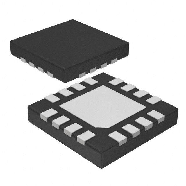
Product Sample & Technical Tools & Support & Folder Buy Documents Software Community LP5521 SNVS441I–JANUARY2007–REVISEDNOVEMBER2016 LP5521 Three-Channel RGB, White-LED Driver With Internal Program Memory and Integrated Charge Pump 1 Features 3 Description • AdaptiveChargePumpWith1× and1.5×Gain The LP5521 is a three-channel LED driver designed 1 to produce variety of lighting effects for mobile ProvidesUpto95%LEDDriveEfficiency devices. A high-efficiency charge pump enables LED • ChargePumpwithSoftStartandOvercurrent, driving over full Li-Ion battery voltage range. The Short-CircuitProtection device has a program memory for creating variety of • LowInputRippleandEMI lighting sequences. When program memory has been loaded, LP5521 can operate autonomously without • VerySmallSolutionSize,NoInductororResistors processorcontrolallowingpowersavings. Required • 200-nATypicalShutdownCurrent The device maintains excellent efficiency over a wide operating range by automatically selecting proper • AutomaticPowerSaveMode charge pump gain based on LED forward voltage • I2C-CompatibleInterface requirements and is able to automatically enter • IndependentlyProgrammableConstantCurrent power-save mode, when LED outputs are not active Outputswith8-BitCurrentSettingand8-BitPWM andthusloweringcurrentconsumption. Control Three independent LED channels have accurate • TypicalLEDOutputSaturationVoltage50mVand programmable current sources and PWM control. CurrentMatching1% Each channel has program memory for creating desiredlightingsequenceswithPWMcontrol. • ThreeProgramExecutionEngineswithFlexible InstructionSet The LP5521 has a flexible digital interface. Trigger • AutonomousOperationWithoutExternalControl I/O and a 32-kHz clock input allow synchronization between multiple devices. Interrupt output can be • LargeSRAMProgramMemory used to notify processor, when LED sequence has • TwoGeneralPurposeDigitalOutputs ended. The LP5521 has four pin selectable I2C- compatible addresses. This allows connecting up to 2 Applications four parallel devices in one I2C-compatible bus. GPO and INT pins can be used as a digital control pin for • FunandIndicatorLights otherdevices. • LCDSub-DisplayBacklighting The LP5521 requires only four small, low-cost • KeypadRGBBacklightingandPhoneCosmetics ceramiccapacitors. • Vibra,Speakers,WaveformGenerator Comprehensive application tools are available, • BloodGlucoseMeter including command compiler for easy LED sequence • HandheldPOSTerminals programming. • ElectronicAccessControl DeviceInformation(1) • WhereRGBIndicationisNeeded PARTNUMBER PACKAGE BODYSIZE TypicalApplicationCircuit LP5521TM DSBGA(20) 2.093mm×1.733mm(MAX) CFLY1 CFLY2 LP5521YQ WQFN(24) 5.00mm×4.00mm(NOM) 0.47 µF 0.47 µF (1) For all available packages, see the orderable addendum at CFLY1P CFLY1N CFLY2P CFLY2N COUT theendofthedatasheet. + CIN VDD VOUT 1 µF - 1 µF SCL RGB LED 0...25.5 mA/LED SDA R EN LP5521 MCU CLK_32K G INT B TRIG ADDR_SEL0 GPO ADDR_SEL1 GNDs Copyright © 2016, Texas Instruments Incorporated 1 An IMPORTANT NOTICE at the end of this data sheet addresses availability, warranty, changes, use in safety-critical applications, intellectualpropertymattersandotherimportantdisclaimers.PRODUCTIONDATA.
LP5521 SNVS441I–JANUARY2007–REVISEDNOVEMBER2016 www.ti.com Table of Contents 1 Features.................................................................. 1 7.4 DeviceFunctionalModes........................................18 2 Applications........................................................... 1 7.5 Programming...........................................................19 3 Description............................................................. 1 7.6 RegisterMaps.........................................................28 4 RevisionHistory..................................................... 2 8 ApplicationandImplementation........................ 36 8.1 ApplicationInformation............................................36 5 PinConfigurationandFunctions......................... 3 8.2 TypicalApplications................................................36 6 Specifications......................................................... 5 8.3 InitializationSetup...................................................39 6.1 AbsoluteMaximumRatings .....................................5 9 PowerSupplyRecommendations...................... 40 6.2 ESDRatings..............................................................5 10 Layout................................................................... 40 6.3 RecommendedOperatingConditions.......................5 6.4 ThermalInformation..................................................6 10.1 LayoutGuidelines.................................................40 6.5 ElectricalCharacteristics...........................................6 10.2 LayoutExample....................................................40 6.6 ChargePumpElectricalCharacteristics...................7 11 DeviceandDocumentationSupport................. 41 6.7 LEDDriverElectricalCharacteristics(R,G,B 11.1 DeviceSupport......................................................41 Outputs).....................................................................7 11.2 DocumentationSupport........................................41 6.8 LogicInterfaceCharacteristics..................................7 11.3 ReceivingNotificationofDocumentationUpdates41 6.9 I2CTimingRequirements(SDA,SCL)......................8 11.4 CommunityResources..........................................41 6.10 TypicalCharacteristics............................................9 11.5 Trademarks...........................................................41 7 DetailedDescription............................................ 11 11.6 ElectrostaticDischargeCaution............................41 7.1 Overview.................................................................11 11.7 Glossary................................................................41 7.2 FunctionalBlockDiagram.......................................11 12 Mechanical,Packaging,andOrderable 7.3 FeatureDescription.................................................12 Information........................................................... 41 4 Revision History ChangesfromRevisionH(May2016)toRevisionI Page • Changedwordingoftitle ........................................................................................................................................................ 1 ChangesfromRevisionG(September2014)toRevisionH Page • AddedseveralnewApplications............................................................................................................................................ 1 • ChangedBodySizeofDSBGApackagetoMAXdimensions .............................................................................................. 1 • ChangedHandlingRatingstoESDRatingstable ................................................................................................................. 5 • ChangedR valueforDSBGAfrom50–90°C/Wto70.7°C/WandWQFNfrom37–90°C/Wto38.4°C/W;add θJA additionalthermalinformation................................................................................................................................................ 6 • AddedCommunityResources ............................................................................................................................................. 41 ChangesfromRevisionF(February2013)toRevisionG Page • AddedPinConfigurationandFunctionssection,HandlingRatingtable,FeatureDescriptionsection,Device FunctionalModes,ApplicationandImplementationsection,PowerSupplyRecommendationssection,Layout section,DeviceandDocumentationSupportsection,andMechanical,Packaging,andOrderableInformation section ................................................................................................................................................................................... 1 2 SubmitDocumentationFeedback Copyright©2007–2016,TexasInstrumentsIncorporated ProductFolderLinks:LP5521
LP5521 www.ti.com SNVS441I–JANUARY2007–REVISEDNOVEMBER2016 5 Pin Configuration and Functions YFQPackage 20-PinDSBGA YFQPackage TopView 20-PinDSBGA BottomView 4 C2FPLY C1FPLY VDD GND TRIG TRIG GND VDD CFLY CFLY 4 1P 2P 3 C2FNLY C1FNLY GND C32LKK INT INT CLK GND CFLY CFLY 3 32K 1N 2N ADDR ADDR 2 VOUT SEL1 SEL0 GPO EN EN GPO ADDR ADDR VOUT 2 SEL0 SEL1 1 B G R SCL SDA 1 SDA SCL R G B A B C D E E D C B A NJAPackage 24-PinWQFN NJAPackage TopView 24-PinWQFN BottomView 19 18 17 16 15 14 13 13 14 15 16 17 18 19 20 12 12 20 21 11 11 21 22 10 10 22 23 9 9 23 24 8 8 24 1 2 3 4 5 6 7 7 6 5 4 3 2 1 Pin 1 Pin 1 PinFunctionsLP5521TM PIN TYPE(1) DESCRIPTION NUMBER NAME 1A B A Currentsourceoutput 1B G A Currentsourceoutput 1C R A Currentsourceoutput 1D SCL I I2CSerialinterfaceclockinput 1E SDA I/OD I2CSerialinterfacedatainput/output 2A VOUT A Chargepumpoutput 2B ADDR_SEL1 I I2Caddressselectinput 2C ADDR_SEL0 I I2Caddressselectinput 2D GPO O Generalpurposeoutput 2E EN I Chipenable 3A CFLY2N A Negativeterminalofchargepumpflycapacitor2 3B CFLY1N A Negativeterminalofchargepumpflycapacitor1 3C GND G Ground 3D CLK_32K I 32-kHzclockinput (1) A:AnalogPin,G:GroundPin,P:PowerPin,I:InputPin,I/O:Input/OutputPin,O:OutputPin,OD:OpenDrainPin Copyright©2007–2016,TexasInstrumentsIncorporated SubmitDocumentationFeedback 3 ProductFolderLinks:LP5521
LP5521 SNVS441I–JANUARY2007–REVISEDNOVEMBER2016 www.ti.com PinFunctionsLP5521TM(continued) PIN TYPE(1) DESCRIPTION NUMBER NAME 3E INT OD/O Interruptoutput/GeneralPurposeOutput 4A CFLY2P A Positiveterminalofchargepumpflycapacitor2 4B CFLY1P A Positiveterminalofchargepumpflycapacitor1 4C VDD P Powersupplypin 4D GND G Ground 4E TRIG I/OD Triggerinput/output PinFunctionsLP5521YQ PIN TYPE(1) DESCRIPTION NUMBER NAME 1 CFLY2P A Positivepinofchargepumpflycapacitor2 2 CFLY1P A Positivepinofchargepumpflycapacitor1 3 VDD P Powersupplypin 4 GND G Ground 5 CLK_32K I 32-kHzclockinput 6 INT OD/O Interruptoutput/Generalpurposeoutput 7 TRIG I/OD Triggerinput/output 8 N/C 9 N/C 10 N/C 11 N/C 12 N/C 13 SDA I/OD I2Cserialinterfacedatainput/output 14 EN I Chipenable 15 SCL I I2CSerialinterfaceclockinput 16 GPO O Generalpurposeoutput 17 R A Currentsourceoutput 18 G A Currentsourceoutput 19 B A Currentsourceoutput 20 ADDR_SEL0 I I2Caddressselectinput 21 ADDR_SEL1 I I2Caddressselectinput 22 VOUT A Chargepumpoutput 23 CFLY2N A Negativepinofchargepumpflycapacitor2 24 CFLY1N A Negativepinofchargepumpflycapacitor1 (1) A:AnalogPin,G:GroundPin,P:PowerPin,I:InputPin,I/O:Input/OutputPin,O:OutputPin,OD:OpenDrainPin 4 SubmitDocumentationFeedback Copyright©2007–2016,TexasInstrumentsIncorporated ProductFolderLinks:LP5521
LP5521 www.ti.com SNVS441I–JANUARY2007–REVISEDNOVEMBER2016 6 Specifications 6.1 Absolute Maximum Ratings overoperatingfree-airtemperaturerange(unlessotherwisenoted)(1)(2)(2)(3) MIN MAX UNIT V(V ,V ,R,G,B) –0.3 6 V DD OUT Voltageonlogicpins –0.3 V +0.3with6Vmaximum V DD Continuouspowerdissipation(4) InternallyLimited Junctiontemperature,T 125 °C J-MAX Maximumleadtemperature(soldering) See(5) Storagetemperature,T –65 150 °C stg (1) StressesbeyondthoselistedunderAbsoluteMaximumRatingsmaycausepermanentdamagetothedevice.Thesearestressratings only,andfunctionaloperationofthedeviceattheseoranyotherconditionsbeyondthoseindicatedunderRecommendedOperating Conditionsisnotimplied.Exposuretoabsolute-maximum-ratedconditionsforextendedperiodsmayaffectdevicereliability. (2) AllvoltagesarewithrespecttothepotentialattheGNDpins. (3) IfMilitary/Aerospacespecifieddevicesarerequired,contacttheTexasInstrumentsSalesOffice/Distributorsforavailabilityand specifications. (4) Internalthermalshutdowncircuitryprotectsthedevicefrompermanentdamage.ThermalshutdownengagesatT =150°C(typical)and J disengagesatT =130°C(typical). J (5) Fordetailedsolderingspecificationsandinformation,pleaserefertoDSBGAWaferLevelChipScalePackage(SNVA009)orLeadless LeadframePackage(LLP)(SNOA401). 6.2 ESD Ratings VALUE UNIT Human-bodymodel(HBM),perANSI/ESDA/JEDECJS-001(1) ±2000 V(ESD) Electrostaticdischarge Charged-devicemodel(CDM),perJEDECspecificationJESD22- V C101(2) ±200 (1) JEDECdocumentJEP155statesthat500-VHBMallowssafemanufacturingwithastandardESDcontrolprocess. (2) JEDECdocumentJEP157statesthat250-VCDMallowssafemanufacturingwithastandardESDcontrolprocess. 6.3 Recommended Operating Conditions overoperatingfree-airtemperaturerange(unlessotherwisenoted)(1)(2)(2) MIN MAX UNIT V 2.7 5.5 V DD RecommendedchargepumploadcurrentI 0 100 mA OUT Junctiontemperature,T , –30 125 °C J Ambienttemperature,T (3) –30 85 °C A (1) StressesbeyondthoselistedunderAbsoluteMaximumRatingsmaycausepermanentdamagetothedevice.Thesearestressratings only,andfunctionaloperationofthedeviceattheseoranyotherconditionsbeyondthoseindicatedunderRecommendedOperating Conditionsisnotimplied.Exposuretoabsolute-maximum-ratedconditionsforextendedperiodsmayaffectdevicereliability. (2) AllvoltagesarewithrespecttothepotentialattheGNDpins. (3) Inapplicationswherehighpowerdissipationand/orpoorpackagethermalresistanceispresent,themaximumambienttemperaturemay havetobederated.Maximumambienttemperature(T )isdependentonthemaximumoperatingjunctiontemperature(T = A-MAX J-MAX-OP 125°C),themaximumpowerdissipationofthedeviceintheapplication(P ),andthejunction-toambientthermalresistanceofthe D-MAX part/packageintheapplication(R ),asgivenbythefollowingequation:T =T –(R ×P ). θJA A-MAX J-MAX-OP θJA D-MAX Copyright©2007–2016,TexasInstrumentsIncorporated SubmitDocumentationFeedback 5 ProductFolderLinks:LP5521
LP5521 SNVS441I–JANUARY2007–REVISEDNOVEMBER2016 www.ti.com 6.4 Thermal Information LP5521 THERMALMETRIC(1) YFQ(DSBGA) NJA(WQFN) UNIT 20PINS 24PINS R Junction-to-ambientthermalresistance 70.7 38.4 °C/W θJA R Junction-to-case(top)thermalresistance 0.5 27.3 °C/W θJC(top) R Junction-to-boardthermalresistance 12.1 15.4 °C/W θJB ψ Junction-to-topcharacterizationparameter 0.2 0.2 °C/W JT ψ Junction-to-boardcharacterizationparameter 12.0 15.4 °C/W JB R Junction-to-case(bottom)thermalresistance n/a 3.1 °C/W θJC(bot) (1) Formoreinformationabouttraditionalandnewthermalmetrics,seetheSemiconductorandICPackageThermalMetricsapplication report,SPRA953. 6.5 Electrical Characteristics Unlessotherwisenoted,specificationsapplytotheLP5521FunctionalBlockDiagramwith:2.7V≤V ≤5.5V,C =C = DD OUT IN 1μF,C =C =0.47μF;limitsareforT =25°Cunlessspecifiedinthetestconditions.(1)(2)(3) FLY1 FLY2 J SYMBOL PARAMETER TESTCONDITIONS MIN TYP MAX UNIT Standbysupplycurrent EN=0(pin),CHIP_EN=0(bit),external32 0.2 kHzclockrunningornotrunning EN=0(pin),CHIP_EN=0(bit),external32- μA kHzclockrunningornotrunning,–30°C<T < 2 A 85°C EN=1(pin),CHIP_EN=0(bit),external32- 1 μA kHzclocknotrunning EN=1(pin),CHIP_EN=0(bit),external32- 1.4 μA kHzclockrunning IVDD Normalmodesupplycurrent ChargepumpandLEDdriversdisabled 0.25 mA Chargepumpin1xmode,noload,LEDdrivers 0.7 mA disabled Chargepumpin1.5xmode,noload,LED 1.5 mA driversdisabled Chargepumpin1xmode,noload,LEDdrivers 1.2 mA enabled Powersavemodesupply External32-kHzclockrunning 10 μA current Internaloscillatorrunning 0.25 mA Internaloscillatorfrequency –4% 4% ƒ OSC accuracy –30°C<T <85°C –7% 7% A (1) AllvoltagesarewithrespecttothepotentialattheGNDpins. (2) MinimumandMaximumlimitsarespecifiedbydesign,test,orstatisticalanalysis. (3) Low-ESRSurface-MountCeramicCapacitors(MLCCs)usedinsettingelectricalcharacteristics. 6 SubmitDocumentationFeedback Copyright©2007–2016,TexasInstrumentsIncorporated ProductFolderLinks:LP5521
LP5521 www.ti.com SNVS441I–JANUARY2007–REVISEDNOVEMBER2016 6.6 Charge Pump Electrical Characteristics LimitsareforT =25°Cunlessspecifiedinthetestconditions.(1) J SYMBOL PARAMETER TESTCONDITION MIN TYP MAX UNIT R Chargepumpoutput Gain=1.5× 3.5 Ω OUT resistance Gain=1× 1 Ω f Switchingfrequency 1.25 MHz SW –30°C<T <85°C –7% 7% A I Groundcurrent Gain=1.5× 1.2 mA GND Gain=1× 0.5 mA V turn-ontimefromcharge V =3.6V,CHIP_EN=H t OUT DD 100 μs ON pumpoffto1.5xmode I =60mA OUT V Chargepumpoutputvoltage V =3.6V,noload,Gain=1.5× 4.55 V OUT DD (1) Input,output,andflycapacitorsshouldbeofthetypeX5RorX7RlowESRceramiccapacitor. 6.7 LED Driver Electrical Characteristics (R, G, B Outputs) LimitsareforT =25°Cunlessspecifiedinthetestconditions. J SYMBOL PARAMETER TESTCONDITION MIN TYP MAX UNIT I R,G,Bpinleakagecurrent 0.1 µA LEAKAGE –30°C<T <85°C 1 A I Maximumsourcecurrent OutputsR,G,B 25.5 mA MAX I Accuracyofoutputcurrent Outputcurrentsetto17.5mA,V =3.6V –4% 4% OUT DD Outputcurrentsetto17.5mA,V =3.6V, –5% 5% DD –30°C<T <85°C A I Matching(1) I =17.5mA,V =3.6V 1% 2% MATCH OUT DD f LEDPWMswitching PWM_HF=1 LED 558 Hz frequency Frequencydefinedbyinternaloscillator PWM_HF=0 Frequencydefinedby32-kHzclock 256 Hz (internalorexternal) V Saturationvoltage(2) I setto17.5mA 50 100 mV SAT OUT (1) Matchingisthemaximumdifferencefromtheaverageofthethreeoutput'scurrents. (2) SaturationvoltageisdefinedasthevoltagewhentheLEDcurrenthasdropped10%fromthevaluemeasuredatV –1V. OUT 6.8 Logic Interface Characteristics (V(EN)=1.65V...V ,andlimitsapplythroughambienttemperaturerange–30°C<T <+85°C,unlessotherwisenoted. DD A PARAMETER TESTCONDITIONS MIN TYP MAX UNIT LOGICINPUTEN V Inputlowlevel 0.5 V IL V Inputhighlevel 1.2 V IH I Logicinputcurrent –1 1 µA I t Inputdelay (1) T =25°C 2 µs DELAY J (1) TheI2C-compatiblehostshouldallowatleast1msbeforesendingdatatotheLP5521aftertherisingedgeoftheenableline. Copyright©2007–2016,TexasInstrumentsIncorporated SubmitDocumentationFeedback 7 ProductFolderLinks:LP5521
LP5521 SNVS441I–JANUARY2007–REVISEDNOVEMBER2016 www.ti.com Logic Interface Characteristics (continued) (V(EN)=1.65V...V ,andlimitsapplythroughambienttemperaturerange–30°C<T <+85°C,unlessotherwisenoted. DD A PARAMETER TESTCONDITIONS MIN TYP MAX UNIT LOGICINPUTSCL,SDA,TRIG,CLK_32K V Inputlowlevel 0.2×V(EN) V IL V Inputhighlevel 0.8×V(EN) V IH I Inputcurrent –1 1 µA I ƒ Clockfrequency T =25°C 32 kHz CLK_32K J ƒ Clockfrequency 400 kHz SCL LOGICOUTPUTSDA,TRIG,INT I =3mA(pullupcurrent), OUT 0.3 T =25°C J V Outputlowlevel I =3mA(pull-upcurrent) 0.5 V OL OUT I Outputleakagecurrent 1 µA L LOGICINPUTADDR_SEL0,ADDR_SEL1 V Inputlowlevel 0.2×V V IL DD V Inputhighlevel 0.8×V V IH DD I Inputcurrent –1 1 µA I LOGICOUTPUTGPO,INT(INGPOSTATE) I =3mA,T =25°C 0.3 OUT J V Outputlowlevel I =3mA 0.5 V OL OUT T =25°C V –0.3 J DD V Outputhighlevel I =–2mA V –0.5 V OH OUT DD I Outputleakagecurrent 1 µA L 6.9 I2C Timing Requirements (SDA, SCL) LimitsareforT =25°C(1) J MIN MAX UNIT ƒ Clockfrequency 400 kHz SCL 1 Holdtime(repeated)STARTcondition 0.6 µs 2 Clocklowtime 1.3 µs 3 Clockhightime 600 ns 4 SetuptimeforarepeatedSTARTcondition 600 ns 5 Dataholdtime 50 ns 6 Dataset-uptime 100 ns 7 RisetimeofSDAandSCL 20+0.1C 300 ns b 8 FalltimeofSDAandSCL 15+0.1C 300 ns b 9 Set-uptimeforSTOPcondition 600 ns 10 Bus-freetimebetweenaSTOPandaSTARTcondition 1.3 µs C Capacitiveloadforeachbusline 10 200 pF b (1) Verifiedbydesign. Figure1. I2CTimingDiagram 8 SubmitDocumentationFeedback Copyright©2007–2016,TexasInstrumentsIncorporated ProductFolderLinks:LP5521
LP5521 www.ti.com SNVS441I–JANUARY2007–REVISEDNOVEMBER2016 6.10 Typical Characteristics Unlessotherwisespecified:V =3.6V DD Figure2.LEDDriveEfficiencyvsInputVoltageAutomatic Figure3.LEDCurrentvsOutputPinHeadroomVoltage GainChange Figure4.LEDCurrentvsCurrentRegisterCode Figure5.LEDCurrentvsSupplyVoltage Figure6.ChargePumpEfficiencyvsLoadCurrent Figure7.ChargePumpEfficiencyvsInputVoltage1.5x Mode Copyright©2007–2016,TexasInstrumentsIncorporated SubmitDocumentationFeedback 9 ProductFolderLinks:LP5521
LP5521 SNVS441I–JANUARY2007–REVISEDNOVEMBER2016 www.ti.com Typical Characteristics (continued) Unlessotherwisespecified:V =3.6V DD Figure8.ChargePumpOutputVoltagevsLoadCurrent Figure9.ChargePumpOutputVoltagevsInputVoltage AutomaticGainChangefrom1xto1.5x Figure10.ChargePumpAutomaticGainChangeHysteresis Figure11.ChargePumpStart-Upin1.5×Mode:NoLoad Figure12.ChargePumpAutomaticGainChange Figure13.StandbyCurrentvsInputVoltage (LEDV =3.6V) F 10 SubmitDocumentationFeedback Copyright©2007–2016,TexasInstrumentsIncorporated ProductFolderLinks:LP5521
LP5521 www.ti.com SNVS441I–JANUARY2007–REVISEDNOVEMBER2016 7 Detailed Description 7.1 Overview The LP5521 is a three-channel LED driver designed to produce variety of lighting effects for mobile devices. A high-efficiency charge pump enables LED driving over full Li-Ion battery voltage range. The device has a program memory for creating variety of lighting sequences. When program memory has been loaded, the LP5521canoperateautonomouslywithoutprocessorcontrolallowingpowersavings. The device maintains excellent efficiency over a wide operating range by automatically selecting proper charge pump gain based on LED forward voltage requirements. the LP5521 is able to automatically enter power-save mode,whenLEDoutputsarenotactiveandthusloweringcurrentconsumption. Three independent LED channels have accurate programmable current sources and PWM control. Each channel hasprogrammemoryforcreatingdesiredlightingsequenceswithPWMcontrol. The LP5521 has a flexible digital interface. A trigger I/O and 32-kHz clock input allow synchronization between multiple devices. Interrupt output can be used to notify processor, when LED sequence has ended. LP5521 has four pin-selectable I2C-compatible addresses. This allows connecting up to four parallel devices in one I2C- compatiblebus.GPOandINTpinscanbeusedasadigitalcontrolpinforotherdevices. TheLP5521requiresonlyfoursmallandlow-costceramiccapacitors. Comprehensive application tools are available, including command compiler for easy LED sequence programming. 7.2 Functional Block Diagram CFLY1 CFLY2 0.47 µF 0.47 µF REF TSD CLK CHARGE PUMP VOUT POR DET 1x/1.5x VDD COUT + CIN BIAS OSC 1 µF - 1 µF PROGRAM MEMORY Command based ADDR_SEL0 PWM pattern generator ADDR_SEL1 VDD_ IO IDAC SCL I2C VDD SDA EN VOUT R Control MCU CLK_32K D INT A VOUT G TRIG VOUT B GPO LP5521 GND Copyright © 2016, Texas Instruments Incorporated Copyright©2007–2016,TexasInstrumentsIncorporated SubmitDocumentationFeedback 11 ProductFolderLinks:LP5521
LP5521 SNVS441I–JANUARY2007–REVISEDNOVEMBER2016 www.ti.com 7.3 Feature Description 7.3.1 ChargePumpOperationalDescription The LP5521 includes a pre-regulated switched-capacitor charge pump with a programmable voltage multiplicationof1and1.5×. In 1.5× mode by combining the principles of a switched-capacitor charge pump and a linear regulator, the device generates a regulated 4.5-V output from Li-Ion input voltage range. A two-phase non-overlapping clock generated internally controls the operation of the charge pump. During the charge phase, both flying capacitors (C and C ) are charged from input voltage. In the pump phase that follows, the flying capacitors are FLY1 FLY2 discharged to output. A traditional switched capacitor charge pump operating in this manner uses switches with very low on-resistance, ideally 0 Ω, to generate an output voltage that is 1.5× the input voltage. The LP5521 regulates the output voltage by controlling the resistance of the input-connected pass-transistor switches in the chargepump. 7.3.1.1 OutputResistance Atlowerinputvoltages,thechargepumpoutputvoltagemaydegradeduetoeffectiveoutputresistance(R )of OUT the charge pump. The expected voltage drop can be calculated by using a simple model for the charge pump showninFigure14. Charge Pump VIN 9¶ 1.5 [(cid:3)9¶ VOUT REG 1.5 x R OUT Copyright © 2016, Texas Instruments Incorporated Figure14. ChargePumpBlockDiagram The model shows a linear pre-regulation block (REG), a voltage multiplier (1.5×), and an output resistance (R ). Output resistance models the output voltage drop that is inherent to switched capacitor converters. The OUT output resistance is 3.5 Ω (typical) and is function of switching frequency, input voltage, capacitance value of the flying capacitors, internal resistances of switches, and ESR of flying capacitors. When the output voltage is in regulation, the regulator in the model controls the voltage V’ to keep the output voltage equal to 4.5 V (typical). With increased output current, the voltage drop across R increases. To prevent drop in output voltage, the OUT voltage drop across the regulator is reduced, V’ increases, and V remains at 4.5 V. When the output current OUT increases to the point that there is zero voltage drop across the regulator, V’ equals the input voltage, and the output voltage is on the edge of regulation. Additional output current causes the output voltage to fall out of regulation, so that the operation is similar to a basic open-loop 1.5× charge pump. In this mode, output current results in output voltage drop proportional to the output resistance of the charge pump. The out-of-regulation outputvoltagecanbeapproximatedby:V =1.5×V – I ×R . OUT IN OUT OUT 7.3.1.2 ControllingChargePump ThechargepumpiscontrolledwithtwoCP_MODEbitsinregister08H.Whenbothbitsarelow,thechargepump is disabled, and the output voltage is pulled down with 300 kΩ. Charge pump can be forced to bypass mode, so that battery voltage is going directly to RGB outputs. In 1.5× mode output voltage is boosted to 4.5 V. In automatic mode, charge pump operation mode is defined by LED outputs saturation described in LED Forward VoltageMonitoring.Table1listsoperationmodesandselectionbits. Table1.CONFIGRegister(08H) NAME BIT DESCRIPTION CP_MODE 4:3 Chargepumpoperationmode 00b=OFF 01b=Forcedtobypassmode(1×) 10b=Forcedto1.5×mode 11b=Automaticmodeselection 12 SubmitDocumentationFeedback Copyright©2007–2016,TexasInstrumentsIncorporated ProductFolderLinks:LP5521
LP5521 www.ti.com SNVS441I–JANUARY2007–REVISEDNOVEMBER2016 7.3.1.3 LEDForwardVoltageMonitoring When charge pump automatic mode selection is enabled, voltages over LED drivers are monitored. If drivers do not have enough headroom, charge pump gain is set to 1.5×. Driver saturation monitor does not have a fixed voltage limit, since saturation voltage is a function of temperature and current. Charge pump gain is set to 1×, whenbatteryvoltageishighenoughtosupplyallLEDs. In automatic gain change mode, charge pump is switched to bypass mode (1×), when LEDs are inactive for over 50ms. Charge pump gain control utilizes digital filtering to prevent supply voltage disturbances from triggering gain changes. If the R driver current source is connected to a battery (address 08H, bit R_TO_BATT = 1), voltage monitoringisdisabledinRoutput,butstillfunctionalinBandGoutputs. LEDforwardvoltagemonitoringandgaincontrolblockdiagramisshowninFigure15. VOUT PWM Charge Current Pump Source MODE VOFS Saturation - Monitor R/G/B + Comparator - Digital Filter Control Registers Program Command Mode Memory Look-ahead Control Copyright © 2016, Texas Instruments Incorporated Figure15. VoltageMonitoringBlockDiagramforOneOutput 7.3.2 LEDDriverOperationalDescription The LP5521 LED drivers are constant current sources with 8-bit PWM control. Output current can be programmedwithI2Cregisterupto25.5mA.Currentsettingresolutionis100μA(8-bitcontrol). R driver has two modes: current source can be connected to the battery (V ) or to the charge pump output. If a DD current source is connected to the battery, automatic charge pump gain control is not used for this output. This approach provides better efficiency when LED with low V is connected to R driver, and battery voltage is high F enough to drive this LED in all conditions. R driver mode can be selected with I2C register bit. When address 08H, bit R_TO_BATT = 1, R current source is connected to battery. When it is 0 (default), R current source is connected to charge pump same way as in G and B drivers. G and B drivers are always connected to charge pumpoutput. Some LED configuration examples are given in Table 2. When LEDs with low V are used, charge pump can be F operating in bypass mode (1×). This eliminates the need of having double drivers for all outputs; one connected tobatteryandanotherconnectedtochargepumpoutput.WhenLP5521isdrivingaRGBLED,Rchannelcanbe configured to use battery power. This configuration increases power efficiency by minimizing the voltage drop acrosstheLEDdriver. Table2.LEDConfigurationExamples CONFIGURATION ROUTPUTTOBATT ROUTPUTTOCP CPMODE RGBLEDwithlowV red X Auto(1×or1.5×) F 3×lowV LED X 1× F 3×whiteLED X Auto(1×or1.5×) 1×lowV LED(Routput) X Disabled F Copyright©2007–2016,TexasInstrumentsIncorporated SubmitDocumentationFeedback 13 ProductFolderLinks:LP5521
LP5521 SNVS441I–JANUARY2007–REVISEDNOVEMBER2016 www.ti.com PWM frequency is either 256 Hz or 558 Hz, frequency is set with PWM_HF bit in register 08H. When PWM_HF is 0, the frequency is 256 Hz, and when bit is 1, the PWM frequency is 558 Hz. Brightness adjustment is either linear or logarithmic. This can be set with register 00H LOG_EN bit. When LOG_EN = 0 linear adjustment scale is used, and when LOG_EN = 1 logarithmic scale is used. By using logarithmic scale the visual effect seems lineartotheeye.RegistercontrolbitsarepresentedinTable3,Table4,andTable5: Table3.R_CURRENTRegister(05H),G_CURRENTregister(06H),B_CURRENTregister(07H): NAME BIT DESCRIPTION CURRENT 7:0 Currentsetting bin hex dec mA 00000000 00 0 0.0 00000001 01 1 0.1 00000010 02 2 0.2 00000011 03 3 0.3 00000100 04 4 0.4 00000101 05 5 0.5 00000110 06 6 0.6 ... ... ... ... 10101111 AF 175 17.5(def) ... ... ... ... 11111011 FB 251 25.1 11111100 FC 252 25.2 11111101 FD 253 25.3 11111110 FE 254 25.4 11111111 FF 255 25.5 Table4.ENABLERegister(00H): NAME BIT DESCRIPTION LOG_EN 7 LogarithmicPWMadjustmentenablebit 0=Linearadjustment 1=Logarithmicadjustment Table5.CONFIGRegister(08H): NAME BIT DESCRIPTION PWM_HF 6 PWMclockfrequency 0=256Hz,frequencydefinedbythe32-kHzclock(internalorexternal) 1=558Hz,frequencydefinedbyinternaloscillator 100 95 90 85 80 75 70 65 % 60 SS 55 E HTN 50 LOG_EN = 0 G 45 RI B 40 LOG_EN = 1 35 30 25 20 15 10 5 0 0 16 32 48 64 80 96 112128 144 160176 192 208 224 240255 CONTROL (DEC) Figure16. LogarithmicandLinearPWMAdjustmentCurves 14 SubmitDocumentationFeedback Copyright©2007–2016,TexasInstrumentsIncorporated ProductFolderLinks:LP5521
LP5521 www.ti.com SNVS441I–JANUARY2007–REVISEDNOVEMBER2016 7.3.3 AutomaticPowerSave Automatic power save mode is enabled when PWRSAVE_EN bit in register address 08H is 1. Almost all analog blocks are powered down in power save, if external clock is used. Only charge pump protection circuits remain active. However if internal clock has been selected only charge pump and led drivers are disabled during power save since digital part of the LED controller need to remain active. In both cases charge pump enters 'weak 1×' mode. In this mode charge pump utilizes a passive current limited keep-alive switch, which keeps the output voltageatbatterylevel. During program execution LP5521 can enter power save if there is no PWM activity in R, G and B outputs. To preventshortpowersavesequencesduringprogramexecution,LP5521hascommandlook-aheadfilter.Inevery instruction cycle R, G, B commands are analyzed, and if there is sufficient time left with no PWM activity, the device enters power save. In power save program execution continues uninterruptedly. When a command that requires PWM activity is executed, fast internal start-up sequence will be started automatically. Table 6 describe commandsandconditionsthatcanactivatepowersave.Allchannels(R,G,B)needtomeetpowersavecondition inordertoenablepowersave. Table6.LEDControllerOperation LEDCONTROLLEROPERATION POWERSAVECONDITION MODE(R,G,B_MODE) 00b Disabledmodeenablespowersave 01b LoadprogramtoSRAMmodepreventspowersave RunprogrammodeenablespowersaveifthereisnoPWMactivityandcommand 10b look-aheadfilterconditionismet 11b DirectcontrolmodeenablespowersaveifthereisnoPWMactivity COMMAND POWERSAVECONDITION NoPWMactivityandcurrentcommandwaittimelongerthan50ms.Ifprescale=1 Wait thenwaittimeneedstobelongerthan80ms. RampCommandPWMvaluereachesminimum0andcurrentcommandexecution Ramp timeleftmorethan50ms.Ifprescale=1thentimeleftneedstobemorethan80ms. Trigger NoPWMactivityduringwaitfortriggercommandexecution. End NoPWMactivityorResetbit=1 SetPWM EnablespowersaveifPWMsetto0andnextcommandgeneratesatleast50mswait Othercommands Noeffecttopowersave SeeapplicationnoteLP5521PowerEfficiencyConsiderations(SNVA185)formoreinformation. 7.3.4 ExternalClockDetection The presence of external clock can be detected by the LP5521. Program execution is clocked with internal 32 kHz clock or with external clock. Clocking is controlled with register address 08H bits, INT_CLK_EN and CLK_DET_ENasseenonthefollowingtable. External clock can be used if clock is present at CLK_32K pin. External clock frequency must be 32 kHz for the program execution / PWM timing to be like specified. If higher or lower frequency is used, it will affect the program engine execution speed. If other than 32 kHz clock frequency is used, the program execution timings must be scaled accordingly. The external clock detector block only detects too low clock frequency (< 15 kHz). If external clock frequency is higher than specified, the external clock detector notifies that external clock is present.ExternalclockstatuscanbecheckedwithreadonlybitEXT_CLK_USEDinregisteraddress0CH,when the external clock detection is enabled (CLK_DET_EN bit = high). If EXT_CLK_USED = 1, then the external clockisdetectedanditisusedfortiming,ifautomaticclockselectionisenabled(seeTable7). If external clock is stuck-at-zero or stuck-at-one, or the clock frequency is too low, the clock detector indicates thatexternalclockisnotpresent. If external clock is not used on the application, connect the CLK_32K pin to GND to prevent floating of this pin andextracurrentconsumption. Copyright©2007–2016,TexasInstrumentsIncorporated SubmitDocumentationFeedback 15 ProductFolderLinks:LP5521
LP5521 SNVS441I–JANUARY2007–REVISEDNOVEMBER2016 www.ti.com Table7.CONFIGRegister(08H): NAME BIT DESCRIPTION LEDcontrollerclocksource 00b=Externalclocksource(CLK_32K) CLK_DET_EN, 1:0 01b=Internalclock INT_CLK_EN 10b=Automaticselection 11b=Internalclock 7.3.5 LogicInterfaceOperationalDescription LP5521 features a flexible logic interface for connecting to processor and peripheral devices. Communication is done with I2C compatible interface and different logic input/output pins makes it possible to synchronize operationofseveraldevices. 7.3.5.1 I/OLevels I2C interface, CLK_32K and TRIG pins input levels are defined by EN pin. Using EN pin as voltage reference for logic inputs simplifies PWB routing and eliminates the need for dedicated V pin. Figure 17 describes EN pin IO connections. VDD Input Buffer EN Level Shifter SDA Level Shifter SCL Copyright © 2016, Texas Instruments Incorporated Figure17. UsingENPinasDigitalI/OVoltageReference ADDR_SEL0/1arereferencedtoV voltage.GPOpinlevelisdefinedbyV voltage. DD DD 7.3.5.2 GPO/INTPins LP5521 has one General Purpose Output pin (GPO); the INT pin can also be configured as a GPO pin. When INT is configured as GPO output, its level is defined by the V voltage. State of the pins can be controlled with DD GPOregister(0EH).GPOpinsaredigitalCMOSoutputsandnopulluporpulldownresistorsareneeded. When INT pin GPO function is disabled, it operates as an open drain pin. INT signal is active low; that is, when interruptsignalissent,thepinispulledtoGND.Externalpullupresistorisneededforproperfunctionality. Table8.GPORegister(0EH) NAME BIT DESCRIPTION EnableINTpinGPOfunction INT_AS_GPO 2 0=INTpinfunctionsasaINTpin 1=INTpinfunctionsasaGPOpin 0=GPOpinstateislow GPO 1 1=GPOpinstateishigh 0=INTpinstateislow(INT_AS_GPO=1) INT 0 1=INTpinstateishigh(INT_AS_GPO=1) 16 SubmitDocumentationFeedback Copyright©2007–2016,TexasInstrumentsIncorporated ProductFolderLinks:LP5521
LP5521 www.ti.com SNVS441I–JANUARY2007–REVISEDNOVEMBER2016 7.3.5.3 TRIGPin The TRIG pin can function as an external trigger input or output. External trigger signal is active low; that is, when trigger is sent or received the pin is pulled to GND. TRIG is an open-drain pin and external pullup resistor is needed for trigger line. External trigger input signal must be at least two 32-kHz clock cycles long to be recognized. Trigger output signal is three 32-kHz clock cycles long. If TRIG pin is not used on application, connectedtheTRIGpintoGNDtopreventfloatingofthispinandextracurrentconsumption. 7.3.5.4 ADDR_SEL0,1Pins TheADDR_SEL0,1pinsdefinethechipI2Caddress.PinsarereferencedtoV signallevel.SeeI2C-Compatible DD SerialBusInterface forI2Caddressdefinitions. 7.3.5.5 CLK_32KPin The CLK_32K pin is used for connecting an external 32-kHz clock to LP5521. External clock can be used to synchronize the sequence engines of several LP5521. Using external clock can also improve automatic power save mode efficiency, because internal clock can be switched off automatically when device has entered power save mode, and external clock is present. See application note LP5521 Power Efficiency Considerations (SNVA185)formoreinformation. Device can be used without the external clock. If external clock is not used on the application, connect the CLK_32KpintoGNDtopreventfloatingofthispinandextracurrentconsumption. Copyright©2007–2016,TexasInstrumentsIncorporated SubmitDocumentationFeedback 17 ProductFolderLinks:LP5521
LP5521 SNVS441I–JANUARY2007–REVISEDNOVEMBER2016 www.ti.com 7.4 Device Functional Modes 7.4.1 ModesofOperation RESET: IntheRESETmodealltheinternalregistersareresettothedefaultvalues.Resetisdonealwaysif ResetRegister(0DH)iswrittenFFHorinternalpoweronreset(POR)isactivated.PORactivates whensupplyvoltageisconnectedorwhenthesupplyvoltageV fallsbelow1.5Vtypical(0.8V DD minimum).OnceV risesabove1.5V,PORinactivates,andthechipcontinuestotheSTANDBY DD mode.CHIP_ENcontrolbitislowafterPORbydefault. STANDBY: TheSTANDBYmodeisenterediftheregisterbitCHIP_ENorENpinisLOWandResetisnot active.Thisisthelowpowerconsumptionmode,whenallcircuitfunctionsaredisabled.Registers canbewritteninthismodeifENpinishigh.Controlbitsareeffectiveafterstart-up. START-UP: WhenCHIP_ENbitiswrittenhighandENpinishigh,theINTERNALSTARTUPSEQUENCE powersupalltheneededinternalblocks(V ,bias,oscillator,etc.).Start-updelayisaftersetting REF ENpinhighis1ms(typical).Start-updelayaftersettingCHIP_ENto1is500 μs(typical).Ifthe chiptemperaturerisestoohigh,thethermalshutdown(TSD)disablesthechipoperation,andthe chipstateisinSTART-UPmodeuntilnoTSDeventispresent.(1) NORMAL: DuringNORMALmodetheusercontrolsthechipusingtheControlRegisters.IfENpinissetlow, theCHIP_ENbitisresetto0. POWERSAVE:InPOWERSAVEmodeanalogblocksaredisabledtominimizepowerconsumption.See AutomaticPowerSaveforfurtherinformation. POR RESET I2C reset=H and EN=H (pin) or POR=H STANDBY EN=H (pin) and CHIP_EN=H (bit) EN=L (pin) or CHIP_EN=L (bit) INTERNAL STARTUP SEQUENCE TSD = H TSD = L NORMAL MODE Enter power save Exit power save POWER SAVE Figure18. ModesofOperation (1) Internalthermalshutdowncircuitryprotectsthedevicefrompermanentdamage.ThermalshutdownengagesatT =150°C(typical)and J disengagesatT =130°C(typical). J 18 SubmitDocumentationFeedback Copyright©2007–2016,TexasInstrumentsIncorporated ProductFolderLinks:LP5521
LP5521 www.ti.com SNVS441I–JANUARY2007–REVISEDNOVEMBER2016 7.5 Programming 7.5.1 I2C-CompatibleSerialBusInterface 7.5.1.1 InterfaceBusOverview The I2C compatible synchronous serial interface provides access to the programmable functions and registers on the device. This protocol uses a two-wire interface for bidirectional communications between the IC's connected to the bus. The two interface lines are the serial data line (SDA), and the serial clock line (SCL). These lines shouldbeconnectedtoapositivesupply,viaapullupresistorandremainHIGHevenwhenthebusisidle. Every device on the bus is assigned a unique address and acts as either a Master or a Slave depending on whetheritgeneratesorreceivestheserialclock(SCL). 7.5.1.2 DataTransactions One data bit is transferred during each clock pulse. Data is sampled during the high state of the serial clock (SCL). Consequently, throughout the high period of the clock the data should remain stable. Any changes on the SDA line during the high state of the SCL and in the middle of a transaction, aborts the current transaction. New data should be sent during the low SCL state. This protocol permits a single data line to transfer both command/controlinformationanddatausingthesynchronousserialclock. SCL SDA data data data data data change valid change valid change allowed allowed allowed Figure19. DataValidity Each data transaction is composed of a start condition, a number of byte transfers (set by the software) and a stop condition to terminate the transaction. Every byte written to the SDA bus must be 8 bits long and is transferred with the most significant bit first. After each byte, an acknowledge signal must follow. The following sectionsprovidefurtherdetailsofthisprocess. Transmitter Stays off the Outputnsmitter AcknBouwsle Ddugrein Cgl othcek Data y Tra b a OutputReceiver Acknowfrolemd gRee Sceigivnearl Datby L C 1 2 3...6 7 8 9 S S Start Condition Figure20. AcknowledgeSignal The Master device on the bus always generates the start and stop conditions (control codes). After a start condition is generated, the bus is considered busy and it retains this status until a certain time after a stop condition is generated. A high-to-low transition of the data line (SDA) while the clock (SCL) is high indicates a startcondition.Alow-to-hightransitionoftheSDAlinewhiletheSCLishighindicatesastopcondition. Copyright©2007–2016,TexasInstrumentsIncorporated SubmitDocumentationFeedback 19 ProductFolderLinks:LP5521
LP5521 SNVS441I–JANUARY2007–REVISEDNOVEMBER2016 www.ti.com Programming (continued) SDA SCL S P START condition STOP condition Figure21. StartandStopConditions In addition to the first start condition, a repeated start condition can be generated in the middle of a transaction. Thisallowsanotherdevicetobeaccessed,oraregisterreadcycle. 7.5.1.3 AcknowledgeCycle The acknowledge cycle consists of two signals: the acknowledge clock pulse the master sends with each byte transferred,andtheacknowledgesignalsentbythereceivingdevice. The master generates the acknowledge clock pulse on the ninth clock pulse of the byte transfer. The transmitter releases the SDA line (permits it to go high) to allow the receiver to send the acknowledge signal. The receiver must pull down the SDA line during the acknowledge clock pulse and ensure that SDA remains low during the high period of the clock pulse, thus signaling the correct reception of the last data byte and its readiness to receivethenextbyte. 7.5.1.4 AcknowledgeAfterEveryByte Rule The master generates an acknowledge clock pulse after each byte transfer. The receiver sends an acknowledge signalaftereverybytereceived. There is one exception to the acknowledge after every byte rule. When the master is the receiver, it must indicate to the transmitter an end of data by not-acknowledging (negative acknowledge) the last byte clocked out of the slave. This negative acknowledge still includes the acknowledge clock pulse (generated by the master), buttheSDAlineisnotpulleddown. 7.5.1.5 AddressingTransferFormats Each device on the bus has a unique slave address. The LP5521 operates as a slave device with the 7-bit address. The LP5521 I2C address is pin selectable from four different choices. If 8-bit address is used for programming,the8thbitis1forreadand0forwrite.Table9 showsthe8-bitI2Caddresses. Table9.8-BitI2CAddresses ADDR_SEL I2CADDRESSWRITE I2CADDRESSREAD [1:0] (8bits) (8bits) 00 01100100=64H 01100101=65H 01 01100110=66H 01100111=67H 10 01101000=68H 01101001=69H 11 01101010=6AH 01101011=6BH Before any data is transmitted, the master transmits the address of the slave being addressed. The slave device sendsanacknowledgesignalontheSDAline,onceitrecognizesitsaddress. The slave address is the first seven bits after a start condition. The direction of the data transfer (R/W) depends onthebitsentaftertheslaveaddress —theeighthbit. Whentheslaveaddressissent,eachdeviceinthesystemcomparesthisslaveaddresswithitsown.Ifthereisa match, the device considers itself addressed and sends an acknowledge signal. Depending upon the state of the R/Wbit(1:read,0:write),thedeviceactsasatransmitterorareceiver. 20 SubmitDocumentationFeedback Copyright©2007–2016,TexasInstrumentsIncorporated ProductFolderLinks:LP5521
LP5521 www.ti.com SNVS441I–JANUARY2007–REVISEDNOVEMBER2016 MSB LSB ADR6 ADR5 ADR4 ADR3 ADR2 ADR1 ADR0 R/W Bit7 bit6 bit5 bit4 bit3 bit2 bit1 bit0 2 IC SLAVE address (chip address) Figure22. I2CChipAddress 7.5.1.6 ControlRegisterWriteCycle • Masterdevicegeneratesstartcondition. • Masterdevicesendsslaveaddress(7bits)andthedatadirectionbit(r/w=0). • Slavedevicesendsacknowledgesignaliftheslaveaddressiscorrect. • Mastersendscontrolregisteraddress(8bits). • Slavesendsacknowledgesignal. • Mastersendsdatabytetobewrittentotheaddressedregister. • Slavesendsacknowledgesignal. • If master will send further data bytes the control register address is incremented by one after acknowledge signal. • Writecycleendswhenthemastercreatesstopcondition. 7.5.1.7 ControlRegisterReadCycle • Masterdevicegeneratesastartcondition. • Masterdevicesendsslaveaddress(7bits)andthedatadirectionbit(r/w=0). • Slavedevicesendsacknowledgesignaliftheslaveaddressiscorrect. • Mastersendscontrolregisteraddress(8bits). • Slavesendsacknowledgesignal. • Masterdevicegeneratesrepeatedstartcondition. • Mastersendstheslaveaddress(7bits)andthedatadirectionbit(r/w=1). • Slavesendsacknowledgesignaliftheslaveaddressiscorrect. • Slavesendsdatabytefromaddressedregister. • If the master device sends acknowledge signal, the control register address is incremented by one. Slave devicesendsdatabytefromaddressedregister. • Read cycle ends when the master does not generate acknowledge signal after data byte and generates stop condition. ADDRESSMODE <StartCondition> <SlaveAddress><r/w=0>[Ack] <RegisterAddr.>[Ack] <RepeatedStartCondition> DataRead <SlaveAddress><r/w=1>[Ack] [RegisterData]<AckorNAck> …additionalreadsfromsubsequentregisteraddresspossible <StopCondition> <StartCondition> <SlaveAddress><r/w=’0’>[Ack] <RegisterAddr.>[Ack] DataWrite <RegisterData>[Ack] …additionalwritestosubsequentregisteraddresspossible <StopCondition> Copyright©2007–2016,TexasInstrumentsIncorporated SubmitDocumentationFeedback 21 ProductFolderLinks:LP5521
LP5521 SNVS441I–JANUARY2007–REVISEDNOVEMBER2016 www.ti.com <>Datafrommaster[]Datafromslave ack from slave ack from slave ack from slave start MSB Chip id LSB w ack MSB Register Addr LSB ack MSB Data LSB ack stop SCL SDA start id = 011 0010b w ack address = 02H ack address 02H data ack stop Figure23. RegisterWriteFormat When a READ function is to be accomplished, a WRITE function must precede the READ function, as shown in Figure24. ack from slave ack from slave repeated start ack from slave data from slave nack from master start MSB Chip id LSB w MSB Register Addr LSB rs MSB Chip Address LSB r MSB Data LSB stop SCL SDA start id = 011 0010b w ack address = 00H ack rs id = 011 0010b r ack address 00H data nack stop w=write(SDA=0) r=read(SDA=1) ack=acknowledge(SDApulleddownbyeithermasterorslave rs=repeatedstart id=7-bitchipaddress Figure24. RegisterReadFormat 7.5.2 LEDControllerOperationModes Operation modes are defined in register address 01H. Each output channel (R, G, B) operation mode can be configured separately. MODE registers are synchronized to a 32-kHz clock. Delay between consecutive I2C writestoOP_MODEregister(01H)needtobelongerthan153 µs(typical). Table10.OP_MODERegister(01H): NAME BIT DESCRIPTION R_MODE 5:4 Rchanneloperationmode 00b=Disabled,resetRchannelPC 01b=LoadprogramtoSRAM,resetRchannelPC 10b=RunprogramdefinedbyR_EXEC 11b=Directcontrol,resetRchannelPC G_MODE 3:2 Gchanneloperationmode 00b=Disabled,resetGchannelPC 01b=LoadprogramtoSRAM,resetGchannelPC 10b=RunprogramdefinedbyG_EXEC 11b=Directcontrol,resetGchannelPC B_MODE 1:0 Bchanneloperationmode 00b=Disabled,resetBchannelPC 01b=LoadprogramtoSRAM,resetBchannelPC 10b=RunprogramdefinedbyB_EXEC 11b=Directcontrol,resetBchannelPC 22 SubmitDocumentationFeedback Copyright©2007–2016,TexasInstrumentsIncorporated ProductFolderLinks:LP5521
LP5521 www.ti.com SNVS441I–JANUARY2007–REVISEDNOVEMBER2016 7.5.2.1 Disabled Each channel can be configured to disabled mode. LED output current is 0 during this mode. Disabled mode resetsPCofrespectivechannel. 7.5.2.2 LOADProgram LP5521 can store 16 commands for each channel (R, G, B). Each command consists of 16 bits. Because one register has only 8 bits, one command requires two I2C register addresses. In order to reduce program load time LP5521 supports address auto incrementation. Register address is incremented after each 8 data bits. Whole programmemorycanbewritteninoneI2Cwritesequence. Program memory is defined in the LP5521 register table, 10H to 2FH for R channel, 30H to 4FH for G channel and 50H to 6FH for B channel. In order to be able to access program memory at least one channel operation modeneedstobeLOADProgram. Memory writes are allowed only to the channel in LOAD mode. All channels are in hold while one or several channels are in LOAD program mode, and PWM values are frozen for the channels which are not in LOAD mode. Program execution continues when all channels are out of LOAD program mode. LOAD Program mode resetsPCofrespectivechannel. 7.5.2.3 RUNProgram RUN Program mode executes the commands defined in program memory for respective channel (R, G, B). Execution register bits in ENABLE register define how program is executed. Program start position can be programmed to Program Counter register (see the following tables). By manually selecting the PC start value, user can write different lighting sequences to the memory, and select appropriate sequence with the PC register. Ifprogramcounterrunstoend(15)thenextcommandwillbeexecutedfromprogramlocation0. If internal clock is used in the RUN program mode, operation mode needs to be written disabled (00b) before disabling the chip (with CHIP_EN bit or EN pin) to ensure that the sequence starts from the correct program counter(PC)valuewhenrestartingthesequence. PC registers are synchronized to 32 kHz clock. Delay between consecutive I2C writes to PC registers (09H, 0AH, 0BH)needtobelongerthan153 µs(typ.). Note that entering LOAD program or Direct Control Mode from RUN PROGRAM mode is not allowed. Engine execution mode should be set to Hold, and Operation Mode to disabled, when changing operation mode from RUNmode. Table11.RChannelPCRegister(09H),GCHANNELPCRegister(0AH),BCHANNELPCRegister(0BH) NAME BIT DESCRIPTION PC 3:0 Programcountervaluefrom0to15d Table12.ENABLERegister(00H) NAME BIT DESCRIPTION R_EXEC 5:4 Rchannelprogramexecution 00b=Hold:WaituntilcurrentcommandisfinishedthenstopwhileEXECmodeishold.PCcanberead orwrittenonlyinthismode. 01b=Step:ExecuteinstructiondefinedbycurrentRchannelPCvalue,incrementPCandchange R_EXECto00b(Hold) 10b=Run:StartatprogramcountervaluedefinedbycurrentRchannelPCvalue 11b=ExecuteinstructiondefinedbycurrentRchannelPCvalueandchangeR_EXECto00b(Hold) G_EXEC 3:2 Gchannelprogramexecution 00b=Hold:WaituntilcurrentcommandisfinishedthenstopwhileEXECmodeishold.PCcanberead orwrittenonlyinthismode. 01b=Step:ExecuteinstructiondefinedbycurrentGchannelPCvalue,incrementPCandchange G_EXECto00b(Hold) 10b=Run:StartatprogramcountervaluedefinedbycurrentGchannelPCvalue 11b=ExecuteinstructiondefinedbycurrentGchannelPCvalueandchangeG_EXECto00b(Hold) Copyright©2007–2016,TexasInstrumentsIncorporated SubmitDocumentationFeedback 23 ProductFolderLinks:LP5521
LP5521 SNVS441I–JANUARY2007–REVISEDNOVEMBER2016 www.ti.com Table12.ENABLERegister(00H)(continued) NAME BIT DESCRIPTION B_EXEC 1:0 Bchannelprogramexecution 00b=Hold:WaituntilcurrentcommandisfinishedthenstopwhileEXECmodeishold.PCcanberead orwrittenonlyinthismode. 01b=Step:ExecuteinstructiondefinedbycurrentBchannelPCvalue,incrementPCandchange B_EXECto00b(Hold) 10b=Run:StartatprogramcountervaluedefinedbycurrentBchannelPCvalue 11b=ExecuteinstructiondefinedbycurrentBchannelPCvalueandchangeB_EXECto00b(Hold) EXEC registers are synchronized to 32-kHz clock. Delay between consecutive I2C writes to ENABLE register (00H)needtobelongerthan488μs(typ.). 7.5.2.3.1 DIRECTControl When R, G or B channel mode is set to 11b, the LP5521 drivers work in direct control mode. LP5521 LED channels can be controlled independently through I2C. For each channel there is a PWM control register and a output current control register. With output current control register is set what is the maximum output current with 8-bit resolution, step size is 100 μA. Duty cycle can be set with 8-bit resolution. Direct control mode resets respectivechannel’sPC.PWMcontrolbitsarepresentedinTable13: Table13.R_PWMRegister(02H),G_PWMRegister(03H),B_PWMRegister(04H): NAME BIT DESCRIPTION PWM 7:0 LEDPWMvalueduringdirectcontroloperationmode 00000000b=0% 11111111b=100% If charge pump automatic gain change is used in this mode, then PWM values need to be written 0 before changingthedrivers’ operationmodetodisabled(00b)toensureproperautomaticgainchangeoperation. 7.5.3 LEDControllerProgrammingCommands LP5521 has three independent programmable channels (R, G, B). Trigger connections between channels are common for all channels. All channels have own program memories for storing complex patterns. Brightness controlandpatternsaredonewith8-bitPWMcontrol(256steps)togetaccurateandsmoothcolorcontrol. Programexecutionistimedwith32768Hzclock.Thisclockcanbegeneratedinternallyorexternal32kHzclock can be connected to CLK_32K pin. Using external clock enables synchronization of LED timing to this clock rather than internal clock. Selection of the clock is made with address 08H bits INT_CLK_EN and CLK_DET_EN. SeeExternalClockDetectionfordetails. Supported commands are listed in Table 14. Command compiler is available for easy sequence programming. With Command compiler it is possible to write sequences with simple ASCII commands, which are then converted to binary or hex format. See application note "LP5521 Programming Considerations"forexamplesofCommandcompilerusage. Table14.LEDControllerProgrammingCommands Command 15 14 13 12 11 10 9 8 7 6 5 4 3 2 1 0 Ramp Pre- 0 Steptime Sign Increment(numberofsteps) Wait scale SetPWM 0 1 0 PWMValue Goto 0 0 0 0 0 0 0 0 0 0 0 Start Branch 1 0 1 Loopcount x Step/commandnumber End 1 1 0 Int Reset X Trigger 1 1 1 Waitfortriggeronchannels5-0 Sendtriggeronchannels5-0 X 24 SubmitDocumentationFeedback Copyright©2007–2016,TexasInstrumentsIncorporated ProductFolderLinks:LP5521
LP5521 www.ti.com SNVS441I–JANUARY2007–REVISEDNOVEMBER2016 Xmeansdonotcarewhether1or0. 7.5.3.1 RAMP/WAIT Ramp command generates a PWM ramp starting from current value. At each ramp step the output is incremented by one. Time for one step is defined with Prescale and Step time bits. Minimum time for one step is 0.49 ms and maximum time is 63 × 15.6 ms = 1 second/step, so it is possible to program very fast and also very slow ramps. Increment value defines how many steps are taken in one command. Number of actual steps is Increment + 1. Maximum value is 127d, which corresponds to half of full scale (128 steps). If during ramp command PWM reaches minimum/maximum (0/255) ramp command is executed to the end, and PWM stays at minimum/maximum. This enables ramp command to be used as combined ramp and wait command in a single instruction. Rampcommandcanbeusedaswaitinstructionwhenincrementiszero. Setting register 00H bit LOG_EN sets the scale from linear to logarithmic. When LOG_EN = 0 linear scale is used, and when LOG_EN = 1 logarithmic scale is used. By using logarithmic scale the visual effect of the ramp commandseemslineartotheeye. Table15.Ramp/WaitCommand 15 14 13 12 11 10 9 8 7 6 5 4 3 2 1 0 Pre- 0 Steptime Sign Increment scale NAME VALUE(d) DESCRIPTION 0 Dividesmasterclock(32768Hz)by16=2048Hz,0.49mscycletime Prescale 1 Dividesmasterclock(32768Hz)by512=64Hz,15.6mscycletime Onerampincrementdonein(steptime)x(clockafterprescale)Note:0meansSet Steptime 1-63 PMWcommand. 0 IncreasePWMoutput Sign 1 DecreasePWMoutput Increment 0-127 ThenumberofstepsisIncrement+1.Note:0isawaitinstruction. Applicationexample: Forexampleiffollowingparametersareusedforramp: • Prescale=1 →cycletime=15.6ms • Steptime=2→time=15.6msx2=31.2ms • Sign=0 →risingramp • Increment=4→5cycles Rampcommandwillbe:0100001000000100b=4204H If current PWM value is 3, and the first command is as described above and next command is a ramp with otherwisesameparameters,butwithSign=1(Command=4284H),theresultwillbelikeinFigure25: PWM Control End of 1st Ramp command, End of 2nd Ramp command, Value start next command start next command Rising ramp, 8 Sign = 0 7 6 Increment = 4 5 => 5 cycles 4 Current value 3 Downward 2 Step time = 31.2 ms ramp, Sign = 1 1 Steps 1 2 3 4 5 6 7 8 9 10 Figure25. Exampleof2SequentialRampCommands. Copyright©2007–2016,TexasInstrumentsIncorporated SubmitDocumentationFeedback 25 ProductFolderLinks:LP5521
LP5521 SNVS441I–JANUARY2007–REVISEDNOVEMBER2016 www.ti.com 7.5.3.2 SetPWM Set PWM output value from 0 to 255. Command takes sixteen 32 kHz clock cycles (= 488 μs). Setting register 00HbitLOG_ENsetsthescalefromlineartologarithmic. Table16.SetPWMCommand 15 14 13 12 11 10 9 8 7 6 5 4 3 2 1 0 0 1 0 0 0 0 0 0 PWMvalue 7.5.3.3 GotoStart Go to start command resets Program Counter register and continues executing program from the 00H location. Command takes sixteen 32 kHz clock cycles. Note that default value for all program memory registers is 0000H, whichisGotostartcommand. Gotostartcommand 15 14 13 12 11 10 9 8 7 6 5 4 3 2 1 0 0 0 0 0 0 0 0 0 0 0 0 0 0 0 0 0 7.5.3.4 Branch When branch command is executed, the 'step number' value is loaded to PC and program execution continues from this location. Looping is done by the number defined in loop count parameter. Nested looping is supported (loopinsideloop).Thenumberofnestedloopsisnotlimited.Commandtakessixteen32-kHzclockcycles. Table17.BranchCommand 15 14 13 12 11 10 9 8 7 6 5 4 3 2 1 0 1 0 1 Loopcount X X X Stepnumber NAME VALUE(d) DESCRIPTION loopcount 0-63 Thenumberofloopstobedone.0meansinfiniteloop. stepnumber 0-15 Thestepnumbertobeloadedtoprogramcounter. 7.5.3.5 End End program execution, resets the program counter and sets the corresponding EXEC register to 00b (hold). Commandtakessixteen32-kHzclockcycles. Table18.EndCommand 15 14 13 12 11 10 9 8 7 6 5 4 3 2 1 0 1 1 0 int reset X X X X X X X X X X X NAME VALUE DESCRIPTION 0 Nointerruptwillbesent. int SendinterrupttoprocessorbypullingtheINTpindownandsettingcorrespondingstatus 1 registerbithightonotifythatprogramhasended.Interruptcanonlybeclearedbyreading interruptstatusregister0CH. 0 KeepthecurrentPWMvalue. reset 1 SetPWMvalueto0. 26 SubmitDocumentationFeedback Copyright©2007–2016,TexasInstrumentsIncorporated ProductFolderLinks:LP5521
LP5521 www.ti.com SNVS441I–JANUARY2007–REVISEDNOVEMBER2016 Xmeansdonotcarewhether1or0. 7.5.3.6 Trigger Wait or send triggers can be used to, for example, synchronize operation between different channels. Send trigger command takes sixteen 32-kHz clock cycles, and wait for trigger takes at least sixteen 32 kHz clock cycles. The receiving channel stores sent triggers. Received triggers are cleared by wait for trigger command if received triggers match to channels defined in the command. Channel waits for until all defined triggers have beenreceived. External trigger input signal must be at least two 32-kHz clock cycles (= 61 μs typical) long to be recognized. Trigger output signal is three 32-kHz clock cycles (92 μs typical) long. External trigger signal is active low; that is, when trigger is sent/received the pin is pulled to GND. Sent external trigger is masked; that is, the device which has sent the trigger does not recognize it. If send and wait external trigger are used on the same command, the sendexternaltriggerisexecutedfirst,thenthewaitexternaltrigger. Table19.TriggerCommand 15 14 13 12 11 10 9 8 7 6 5 4 3 2 1 0 waittrigger<5:0> sendtrigger<5:0> 1 1 1 X EXT X B G R EXT X B G R NAME VALUE(d) DESCRIPTION Waitfortriggerforthechannel(s)defined.Severaltriggerscanbedefinedinthesame waittrigger<5:0> 0-31 command.Bit0isR,bit1isG,bit2isBandbit5isexternaltriggerI/O.Bits3and4 arenotinuse. Sendtriggerforthechannel(s)defined.Severaltriggerscanbedefinedinthesame sendtrigger<5:0> 0-31 command.Bit0isR,bit1isG,bit2isBandbit5isexternaltriggerI/O.Bits3and4 arenotinuse. Xmeansdonotcarewhether1or0. Copyright©2007–2016,TexasInstrumentsIncorporated SubmitDocumentationFeedback 27 ProductFolderLinks:LP5521
LP5521 SNVS441I–JANUARY2007–REVISEDNOVEMBER2016 www.ti.com 7.6 Register Maps Table20.LP5521ControlRegisterNamesandDefaultValues ADDR REGISTER D7 D6 D5 D4 D3 D2 D1 D0 DEFAULT (HEX) 00 ENABLE LOG_EN CHIP_EN R_EXEC[1:0] G_EXEC[1:0] B_EXEC[1:0] 00000000 01 OPMODE R_MODE[1:0] G_MODE[1:0] B_MODE[1:0] 00000000 02 RPWM R_PWM[7:0] 00000000 03 GPWM G_PWM[7:0] 00000000 04 BPWM B_PWM[7:0] 00000000 05 RCURRENT R_CURRENT[7:0] 10101111 06 GCURRENT G_CURRENT[7:0] 10101111 07 BCURRENT B_CURRENT[7:0] 10101111 08 CONFIG PWM_HF PWRSAVE_EN CP_MODE[1:0] R_TO_BATT CLK_DET_EN INT_CLK_EN 00000000 09 RPC R_PC[3:0] 00000000 0A GPC G_PC[3:0] 00000000 0B BPC B_PC[3:0] 00000000 0C STATUS EXT_CLK_USED R_INT G_INT B_INT 00000000 0D RESET RESET[7:0] 00000000 0E GPO INT_AS_GPO GPO INT 00000000 10 PROGMEMR CMD_R1[15:8] 00000000 11 PROGMEMR CMD_R1[7:0] 00000000 ... 2E PROGMEMR CMD_R16[15:8] 00000000 2F PROGMEMR CMD_R16[7:0] 00000000 30 PROGMEMG CMD_G1[15:8] 00000000 31 PROGMEMG CMD_G1[7:0] 00000000 ... 4E PROGMEMG CMD_G16[15:8] 00000000 4F PROGMEMG CMD_G16[7:0] 00000000 50 PROGMEMB CMD_B1[15:8] 00000000 51 PROGMEMB CMD_B1[7:0] 00000000 ... 6E PROGMEMB CMD_B16[15:8] 00000000 6F PROGMEMB CMD_B16[7:0] 00000000 28 SubmitDocumentationFeedback Copyright©2007–2016,TexasInstrumentsIncorporated ProductFolderLinks:LP5521
LP5521 www.ti.com SNVS441I–JANUARY2007–REVISEDNOVEMBER2016 7.6.1 EnableRegister(Enable) Address00H Resetvalue00H Table21.EnableRegister 7 6 5 4 3 2 1 0 LOG_EN CHIP_EN R_EXEC[1] R_EXEC[0] G_EXEC[1] G_EXEC[0] B_EXEC[1] B_EXEC[0] NAME BIT ACCESS ACTIVE DESCRIPTION LOG_EN 7 R/W High LogarithmicPWMadjustmentgenerationenable Masterchipenable.Enablesdeviceinternalstartupsequence.Startupdelay CHIP_EN 6 R/W High aftersettingCHIP_ENis500μs.SeeOperationforfurtherinformation. SettingENpinlowresetstheCHIP_ENstateto0. Rchannelprogramexecution. 00b=Hold:WaituntilcurrentcommandisfinishedthenstopwhileEXEC modeishold.PCcanbereadorwrittenonlyinthismode. 01b=Step:ExecuteinstructiondefinedbycurrentRchannelPCvalue, R_EXEC 5:4 R/W incrementPCandchangeR_EXECto00b(Hold) 10b=Run:StartatprogramcountervaluedefinedbycurrentRChannelPC value 11b=ExecuteinstructiondefinedbycurrentRchannelPCvalueandchange R_EXECto00b(Hold) Gchannelprogramexecution 00b=Hold:WaituntilcurrentcommandisfinishedthenstopwhileEXEC modeishold.PCcanbereadorwrittenonlyinthismode. 01b=Step:ExecuteinstructiondefinedbycurrentGchannelPCvalue, G_EXEC 3:2 R/W incrementPCandchangeG_EXECto00b(Hold) 10b=Run:StartatprogramcountervaluedefinedbycurrentGChannelPC value 11b=ExecuteinstructiondefinedbycurrentGchannelPCvalueand changeG_EXECto00b(Hold) Bchannelprogramexecution 00b=Hold:WaituntilcurrentcommandisfinishedthenstopwhileEXEC modeishold.PCcanbereadorwrittenonlyinthismode. 01b=Step:ExecuteinstructiondefinedbycurrentBchannelPCvalue, B_EXEC 1:0 R/W incrementPCandchangeB_EXECto00b(Hold) 10b=Run:StartatprogramcountervaluedefinedbycurrentBChannelPC value 11b=ExecuteinstructiondefinedbycurrentBchannelPCvalueandchange B_EXECto00b(Hold) EXEC registers are synchronized to 32 kHz clock. Delay between consecutive I2C writes to ENABLE register (00H)needtobelongerthan488μs(typ). Copyright©2007–2016,TexasInstrumentsIncorporated SubmitDocumentationFeedback 29 ProductFolderLinks:LP5521
LP5521 SNVS441I–JANUARY2007–REVISEDNOVEMBER2016 www.ti.com 7.6.2 OperationModeRegister(OPMode) Address01H Resetvalue00H Table22.OPModeRegister 7 6 5 4 3 2 1 0 R_MODE[1] R_MODE[0] G_MODE[1] G_MODE[0] B_MODE[1] B_MODE[0] NAME BIT ACCESS ACTIVE DESCRIPTION Rchanneloperationmode 00b=Disabled R_MODE 5:4 R/W 01b=LoadprogramtoSRAM,resetRchannelPC 10b=RunprogramdefinedbyR_EXEC 11b=Directcontrol Gchanneloperationmode 00b=Disabled G_MODE 3:2 R/W 01b=LoadprogramtoSRAM,resetGchannelPC 10b=RunprogramdefinedbyG_EXEC 11b=Directcontrol Bchanneloperationmode 00b=Disabled B_MODE 1:0 R/W 01b=LoadprogramtoSRAM,resetBchannelPC 10b=RunprogramdefinedbyB_EXEC 11b=Directcontrol MODE registers are synchronized to 32 kHz clock. Delay between consecutive I2C writes to OP_MODE register (01H)needtobelongerthan153μs(typ). 7.6.3 RChannelPWMControl(R_PWM) Address02H Resetvalue00H Table23.RPWMRegister 7 6 5 4 3 2 1 0 R_PWM[7:0] NAME BIT ACCESS ACTIVE DESCRIPTION R_PWM 7:0 R/W RChannelPWMvalueduringdirectcontroloperationmode 30 SubmitDocumentationFeedback Copyright©2007–2016,TexasInstrumentsIncorporated ProductFolderLinks:LP5521
LP5521 www.ti.com SNVS441I–JANUARY2007–REVISEDNOVEMBER2016 7.6.4 GChannelPWMControl(G_PWM) Address03H Resetvalue00H Table24.GPWMRegister 7 6 5 4 3 2 1 0 G_PWM[7:0] NAME BIT ACCESS ACTIVE DESCRIPTION G_PWM 7:0 R/W GChannelPWMvalueduringdirectcontroloperationmode 7.6.5 BChannelPWMControl(B_PWM) Address04H Resetvalue00H Table25.BPWMRegister 7 6 5 4 3 2 1 0 B_PWM[7:0] NAME BIT ACCESS ACTIVE DESCRIPTION B_PWM 7:0 R/W BChannelPWMvalueduringdirectcontroloperationmode 7.6.6 RChannelCurrent(R_CURRENT) Address05H ResetValueAFH Table26.RCURRENTRegister 7 6 5 4 3 2 1 0 R_CURRENT[7:0] NAME BIT ACCESS ACTIVE DESCRIPTION Currentsetting 00000000b=0.0mA 00000001b=0.1mA 00000010b=0.2mA 00000011b=0.3mA 00000100b=0.4mA 00000101b=0.5mA 00000110b=0.6mA R_CURRENT 7:0 R/W ... 10101111b=17.5mA(default) ... 11111011b=25.1mA 11111100b=25.2mA 11111101b=25.3mA 11111110b=25.4mA 11111111b=25.5mA Copyright©2007–2016,TexasInstrumentsIncorporated SubmitDocumentationFeedback 31 ProductFolderLinks:LP5521
LP5521 SNVS441I–JANUARY2007–REVISEDNOVEMBER2016 www.ti.com 7.6.7 GChannelCurrent(G_CURRENT) Address06H ResetValueAFH Table27.GCURRENTRegister 7 6 5 4 3 2 1 0 G_CURRENT[7:0] NAME BIT ACCESS ACTIVE DESCRIPTION Currentsetting 00000000b=0.0mA 00000001b=0.1mA 00000010b=0.2mA 00000011b=0.3mA 00000100b=0.4mA 00000101b=0.5mA 00000110b=0.6mA G_CURRENT 7:0 R/W ... 10101111b=17.5mA(default) ... 11111011b=25.1mA 11111100b=25.2mA 11111101b=25.3mA 11111110b=25.4mA 11111111b=25.5mA 7.6.8 BChannelCurrent(B_CURRENT) Address07H ResetvalueAFH Table28.BCURRENTRegister 7 6 5 4 3 2 1 0 B_CURRENT[7:0] NAME BIT ACCESS ACTIVE DESCRIPTION Currentsetting 00000000b=0.0mA 00000001b=0.1mA 00000010b=0.2mA 00000011b=0.3mA 00000100b=0.4mA 00000101b=0.5mA 00000110b=0.6mA B_CURRENT 7:0 R/W ... 10101111b=17.5mA(default) ... 11111011b=25.1mA 11111100b=25.2mA 11111101b=25.3mA 11111110b=25.4mA 11111111b=25.5mA 32 SubmitDocumentationFeedback Copyright©2007–2016,TexasInstrumentsIncorporated ProductFolderLinks:LP5521
LP5521 www.ti.com SNVS441I–JANUARY2007–REVISEDNOVEMBER2016 7.6.9 ConfigurationControl(CONFIG) Address08H Resetvalue00H Table29.CONFIGRegister 7 6 5 4 3 2 1 0 PWM_HF PWRSAVE_EN CP_MODE[1:0] R_TO_BATT CLK_DET_EN INT_CLK_EN NAME BIT ACCESS ACTIVE DESCRIPTION PWMclock PWM_HF 6 R/W High 0=256HzPWMclockused(CLK_32K) 1=558HzPWMclockused(internaloscillator) PWRSAVE_EN 5 R/W High Powersavemodeenable Chargepumpoperationmode 00b=OFF CP_MODE 4:3 R/W 01b=Forcedtobypassmode(1x) 10b=Forcedto1.5xmode 11b=Automaticmodeselection Rchannelsupplyconnection R_TO_BATT 2 R/W High 0=Routputconnectedtochargepump 1=Routputconnectedtobattery LEDControllerclocksource 00b=Externalclocksource(CLK_32K) CLK_DET_EN, 1:0 R/W 01b=Internalclock INT_CLK_EN 10b=Automaticselection 11b=Internalclock 7.6.10 RChannelProgramCounterValue(RChannelPC) Address09H Resetvalue00H Table30.RChannelPCRegister 7 6 5 4 3 2 1 0 R_PC[3] R_PC[2] R_PC[1] R_PC[0] NAME BIT ACCESS ACTIVE DESCRIPTION R_PC 3:0 R/W Rchannelprogramcountervalue PC registers are synchronized to a 32-kHz clock. Delay between consecutive I2C writes to PC registers needs to belongerthan153μs(typ.).PCregistercanbereadorwrittenonlywhenEXECmodeis'hold'. Copyright©2007–2016,TexasInstrumentsIncorporated SubmitDocumentationFeedback 33 ProductFolderLinks:LP5521
LP5521 SNVS441I–JANUARY2007–REVISEDNOVEMBER2016 www.ti.com 7.6.11 GChannelProgramCounterValue(GChannelPC) Address0AH Resetvalue00H Table31.GChannelPCRegister 7 6 5 4 3 2 1 0 G_PC[3] G_PC[2] G_PC[1] G_PC[0] NAME BIT ACCESS ACTIVE DESCRIPTION G_PC 3:0 R/W Gchannelprogramcountervalue PC registers are synchronized to 32 kHz clock. Delay between consecutive I2C writes to PC registers needs to belongerthan153μs(typ.).PCregistercanbereadorwrittenonlywhenEXECmodeis'hold'. 7.6.12 BChannelProgramCounterValue(BChannelPC) Address0BH Resetvalue00H Table32.BChannelPCRegister 7 6 5 4 3 2 1 0 B_PC[3] B_PC[2] B_PC[1] B_PC[0] NAME BIT ACCESS ACTIVE DESCRIPTION B_PC 3:0 R/W Bchannelprogramcountervalue PC registers are synchronized to a 32-kHz clock. Delay between consecutive I2C writes to PC registers must be longerthan153μs(typ.).PCregistercanbereadorwrittenonlywhenEXECmodeis'hold'. 7.6.13 Status/InterruptRegister Address0CH Resetvalue00H Table33.STATUS/INTERRUPTRegister 7 6 5 4 3 2 1 0 EXT_CLK R_INT G_INT B_INT USED NAME BIT ACCESS ACTIVE DESCRIPTION EXT_CLK Externalclockstate USED 3 R 0=Internal32kHzclockused 1=External32kHzclockused R_INT 2 R High InterruptfromRchannel G_INT 1 R High InterruptfromGchannel B_INT 0 R High InterruptfromBchannel Note: Register INT bits will be cleared when read operation to Status/Interrupt register occurs. INT output pin (activelow)willgohighafterreadoperation. 34 SubmitDocumentationFeedback Copyright©2007–2016,TexasInstrumentsIncorporated ProductFolderLinks:LP5521
LP5521 www.ti.com SNVS441I–JANUARY2007–REVISEDNOVEMBER2016 7.6.14 RESETRegister Address0DH Resetvalue00H Table34.RESETRegister 7 6 5 4 3 2 1 0 RESET RESET RESET RESET RESET RESET RESET RESET NAME BIT ACCESS ACTIVE DESCRIPTION RESET 7:0 W ResetallregistervalueswhenFFHiswritten.NoacknowledgefromLP5521 afterwrite. 7.6.15 GPORegister Address0EH Resetvalue00H Table35.GPORegister 7 6 5 4 3 2 1 0 INT_AS_GPO GPO INT NAME BIT ACCESS ACTIVE DESCRIPTION INT_AS_GPO 2 R/W High EnableINTpinGPOfunction GPOpinstate: GPO 1 R/W High 0=LOW 1=HIGH INTpinstate(whenINT_AS_GPO=1): INT 0 R/W High 0=LOW 1=HIGH 7.6.16 ProgramMemory Address10H–6FH Resetvalues00H PleaseseeLEDControllerProgrammingCommandsforfurtherinformation. Command 15 14 13 12 11 10 9 8 7 6 5 4 3 2 1 0 Ramp Pre- 0 Steptime Sign Increment Wait scale SetPWM 0 1 0 PWMValue GotoStart 0 0 0 0 0 0 0 0 0 0 0 Branch 1 0 1 LoopCount X Stepnumber End 1 1 0 Int Reset X Trigger 1 1 1 Waitfortriggeronchannels5-0 Sendtriggeronchannels5-0 X Copyright©2007–2016,TexasInstrumentsIncorporated SubmitDocumentationFeedback 35 ProductFolderLinks:LP5521
LP5521 SNVS441I–JANUARY2007–REVISEDNOVEMBER2016 www.ti.com 8 Application and Implementation NOTE Information in the following applications sections is not part of the TI component specification, and TI does not warrant its accuracy or completeness. TI’s customers are responsible for determining suitability of components for their purposes. Customers should validateandtesttheirdesignimplementationtoconfirmsystemfunctionality. 8.1 Application Information The LP5521 is designed as a autonomous lighting controller for mobile devices. These devices need extremely small form factor; therefore, the LP5521 is designed to require only 4 small capacitors: input, output, and two fly- capacitors for charge pump. If charge pump is not needed in the application (input voltage is high enough for driving LEDs), the charge pump capacitors can be omitted thus reducing the solution size even further. LED can beRGBLEDoranycolorifdesired. 8.2 Typical Applications Application with Charge Pump shows an example of typical application which uses charge pump to get high enoughvoltagetodriveLEDs.ThedeviceispoweredfromsingleLi-Ionbatterywithvoltagerangeof2.7Vto4.2 V. 8.2.1 ApplicationwithChargePump CFLY1 CFLY2 0.47 µF 0.47 µF CFLY1P CFLY1N CFLY2P CFLY2N COUT 1 µF + CIN VDD VOUT - 1 µF SCL RGB LED 0...25.5 mA/LED SDA R EN LP5521 MCU G CLK_32K INT B TRIG ADDR_SEL0 GPO ADDR_SEL1 GNDs Copyright © 2016, Texas Instruments Incorporated Figure26. LP5521TypicalApplicationSchematicWithChargePump 8.2.1.1 DesignRequirements DESIGNPARAMETER EXAMPLEVALUE Inputvoltagerange 2.7Vto4.2V(singleLi-Ioncellbattery) LEDV (maximum) 3.6V F LEDcurrent 25.5mAmaximum Inputcapacitor C =1μF IN Outputcapacitor C =1μF OUT Flycapacitors C =C =470nF FLY1 FLY2 Chargepumpmode Automaticor1.5× 36 SubmitDocumentationFeedback Copyright©2007–2016,TexasInstrumentsIncorporated ProductFolderLinks:LP5521
LP5521 www.ti.com SNVS441I–JANUARY2007–REVISEDNOVEMBER2016 8.2.1.2 DetailedDesignProcedure 8.2.1.2.1 CapacitorSelection The LP5521 requires 4 external capacitors for proper operation (C = C = 1 μF, C = C = 470 nF). IN OUT FLY1 FLY2 Surface-mount multi-layer ceramic capacitors are recommended. These capacitors are small, inexpensive and have very low equivalent series resistance (ESR < 20 mΩ typical). Tantalum capacitors, OS-CON capacitors, and aluminum electrolytic capacitors are not recommended for use with the LP5521 due to their high ESR, as comparedtoceramiccapacitors. For most applications, ceramic capacitors with X7R or X5R temperature characteristic are preferred for use with the LP5521. These capacitors have tight capacitance tolerance (as good as ±10%) and hold their value over temperature(X7R:±15%over –55°Cto125°C;X5R:±15%over –55°Cto85°C). Capacitors with Y5V or Z5U temperature characteristic are generally not recommended for use with the LP5521. Capacitors with these temperature characteristics typically have wide capacitance tolerance (+80%, –20%) and vary significantly over temperature (Y5V: +22%, –82% over –30°C to +85°C range; Z5U: +22%, –56% over +10°C to +85°C range). Under some conditions, a nominal 1-μF Y5V or Z5U capacitor could have a capacitance of only 0.1 μF. Such detrimental deviation is likely to cause Y5V and Z5U capacitors to fail to meet the minimum capacitancerequirementsoftheLP5521. The minimum voltage rating acceptable for all capacitors is 6.3 V. The recommended voltage rating of the output capacitoris10VtoaccountforDCbiascapacitancelosses. NOTE Someceramiccapacitors,especiallythoseinsmallpackages,exhibitastrongcapacitance reduction with the increased applied voltage (DC bias effect). The capacitance value can fallbelowhalfofthenominalcapacitance.ChooseoutputandinputcapacitorwithDCbias voltageeffectbetterthan –50%at5Vvoltage(0.5 μFat5V). Table36.ExternalComponentExamples MODEL TYPE VENDOR VOLTAGERATING SIZEINCH(mm) 1μFforC andC OUT IN C1005X5R1A105K CeramicX5R TDK 10V 0402(1005) ECJ0EB1A105M CeramicX5R Panasonic 10V 0402(1005) ECJUVBPA105M CeramicX5R,arrayoftwo Panasonic 10V 0504 470nFforC FLY1-2 C1005X5R1A474K CeramicX5R TDK 10V 0402(1005) ECJ0EB0J474K CeramicX5R Panasonic 10V 0402(1005) LEDs UserDefined Copyright©2007–2016,TexasInstrumentsIncorporated SubmitDocumentationFeedback 37 ProductFolderLinks:LP5521
LP5521 SNVS441I–JANUARY2007–REVISEDNOVEMBER2016 www.ti.com 8.2.1.3 ApplicationCurves Figure27.ChargePumpLoadTransientResponsein1.5× Figure28.ChargePumpLineTransientResponse Mode(0to25.5mA) 1.5×Mode(V 3.5Vto4V) IN 8.2.2 ApplicationWithoutChargePump In this application example the input voltage is high enough to drive the LEDs even without charge pump. In that case the charge pump components are omitted, allowing savings on bill-of-material and also board space. Chargepumpmustbesetto1×mode(bypass)inthiscase. CFLY1P CFLY1N CFLY2P CFLY2N + CIN VDD VOUT COUT - 1 PF 1 PF RGB LED 0...25.5 mA/LED SCL SDA R LP5521 EN MCU G CLK_32K INT B TRIG ADDR_SEL0 GPO ADDR_SEL1 GNDs Copyright © 2016, Texas Instruments Incorporated Figure29. TypicalApplicationSchematicWithoutChargePump 8.2.2.1 DesignRequirements DESIGNPARAMETER EXAMPLEVALUE Inputvoltagerange 4.5Vto5.5V LEDV (max) 3.6V F LEDcurrent 25.5mAmaximum Inputcapacitor C =1μF IN Outputcapacitor C =1μF OUT Flycapacitors none Chargepumpmode 1X 38 SubmitDocumentationFeedback Copyright©2007–2016,TexasInstrumentsIncorporated ProductFolderLinks:LP5521
LP5521 www.ti.com SNVS441I–JANUARY2007–REVISEDNOVEMBER2016 8.2.2.2 DetailedDesignProcedures Selectinginputandoutputcapacitorsfollowsthesameprocedureasintheapplicationwithchargepump. 8.3 Initialization Setup 8.3.1 ProgramLoadandExecutionExample 1. StartupDeviceandConfigureDevicetoSRAMWriteMode: – Supplye.g.3.6VtoVDD – Supplye.g.1.8VtoEN – Wait1ms(startupdelay) – Generate32kHzclocktoCLK_32Kpin – Writetoaddress00H01000000b(enableLP5521) – Wait500 μs(startupdelay) – Writetoaddress01H00010000b(ConfigureRchannelinto"LoadprogramtoSRAM"mode) 2. ProgramLoadtoSRAM(seeFigure30): – Writetoaddress10H00000011b(1strampcommand8MSB) – Writetoaddress11H01111111b(1strampcommand8LSB) – Writetoaddress12H01001101b(1stwaitcommand8MSB) – Writetoaddress13H00000000b(1stwaitcommand8LSB) – Writetoaddress14H00000011b(2ndrampcommand8MSB) – Writetoaddress15H11111111b(2ndrampcommand8LSB) – Writetoaddress16H01100000b(2ndwaitcommand8MSB) – Writetoaddress17H00000000b(2ndwaitcommand8LSB) 3. EnablePowersave,chargepumpautomaticmode(1x/1.5x)anduseexternal32kHzclock: – Writetoaddress08H00111000b 4. Runprogram: – Write to address 01H 0010 0000b (Configure LED controller operation mode to "Run program" in R channel – Writetoaddress00H01100000b(Configureprogramexecutionmodefrom"Hold"to"Run"inRchannel LP5521 will generate 1100 ms long LED pattern which will be repeated infinitely. LED pattern is illustrated in Figure30. PWM value 255 R 127 Time (ms) 100 200 300 400 500 600 700 800 900 1000 1100 1200 1300 1400 1500 1600 1700 R program: R program as binary code: ramp up to PWM value 128 in 200 ms 0000001101111111 wait 200 ms 0100110100000000 ramp down to PWM value 0 in 200 ms 0000001111111111 wait 500 ms 0110000000000000 Figure30. SequenceDiagram 8.3.2 DirectPWMControlExample 1. Startupdevice: – Supply,forexample,3.6VtoVDD – Supply,forexample,1.8VtoEN – Wait1ms(start-updelay) – Writetoaddress00H01000000b(enableLP5521) Copyright©2007–2016,TexasInstrumentsIncorporated SubmitDocumentationFeedback 39 ProductFolderLinks:LP5521
LP5521 SNVS441I–JANUARY2007–REVISEDNOVEMBER2016 www.ti.com Initialization Setup (continued) – Wait500 µs(start-updelay) 2. Enablechargepump1.5xmodeanduseinternalclock: – Writetoaddress08H00010001b 3. DirectPWMcontrol: – Writetoaddress01H00111111b(ConfigureR,GandBchannelsinto"DirectPWMcontrolmode") 4. WritePWMvalues: – Writetoaddress02H10000000b(RdriverPWM50%dutycycle) – Writetoaddress03H11000000b(GdriverPWM75%dutycycle) – Writetoaddress04H11111111b(BdriverPWM100%dutycycle) LEDs are turned on after the PWM values are written. Changes to the PWM value registers are reflected immediatelytotheLEDbrightness.DefaultLEDcurrent(17.5mA)isusedforLEDoutputs,ifnoothervaluesare written. 9 Power Supply Recommendations The device is designed to operate from an input voltage supply range between 2.7 V and 5.5V. In a typical application this is from single Li-ion battery cell. This input supply must be well regulated and able to withstand maximum input current and maintain stable voltage without voltage drop even at load transition condition (start- up or rapid brightness change). The resistance of the input supply rail must be low enough that the input current transientdoesnotcausedropbelowa2.7-VlevelintheLP5521supplyvoltage. 10 Layout 10.1 Layout Guidelines Place capacitors as close to the LP5521 device as possible to minimize the current loops. Figure 31 shows an exampleofLP5521PCBlayoutandcomponentplacement. 10.2 Layout Example MicroVias CFLY CFLY VDD GND TRIG 2P 1P C2FNLY C1FNLY GND C32LKK INT Control signals ADDR ADDR VOUT SEL1 SEL0 GPO EN B G R SCL SDA Top Layer Inner Layer Vias to GND plane To LEDs Figure31. ExampleofTypicalLayout 40 SubmitDocumentationFeedback Copyright©2007–2016,TexasInstrumentsIncorporated ProductFolderLinks:LP5521
LP5521 www.ti.com SNVS441I–JANUARY2007–REVISEDNOVEMBER2016 11 Device and Documentation Support 11.1 Device Support 11.1.1 Third-PartyProductsDisclaimer TI'S PUBLICATION OF INFORMATION REGARDING THIRD-PARTY PRODUCTS OR SERVICES DOES NOT CONSTITUTE AN ENDORSEMENT REGARDING THE SUITABILITY OF SUCH PRODUCTS OR SERVICES OR A WARRANTY, REPRESENTATION OR ENDORSEMENT OF SUCH PRODUCTS OR SERVICES, EITHER ALONEORINCOMBINATIONWITHANYTIPRODUCTORSERVICE. 11.2 Documentation Support 11.2.1 RelatedDocumentation • SeeLP5521ProgrammingConsiderationsformoreinformationaboutprogrammingofthedevice. • See LP5521 Power Efficiency Consideration for more information about powering the device and partitioning thesystem. • SeeLP5521TMEvaluationKitformoreinformationaboutevaluationkitforLP5521TM. 11.3 Receiving Notification of Documentation Updates To receive notification of documentation updates, navigate to the device product folder on ti.com. In the upper right corner, click on Alert me to register and receive a weekly digest of any product information that has changed.Forchangedetails,reviewtherevisionhistoryincludedinanyreviseddocument. 11.4 Community Resources The following links connect to TI community resources. Linked contents are provided "AS IS" by the respective contributors. They do not constitute TI specifications and do not necessarily reflect TI's views; see TI's Terms of Use. TIE2E™OnlineCommunity TI'sEngineer-to-Engineer(E2E)Community.Createdtofostercollaboration amongengineers.Ate2e.ti.com,youcanaskquestions,shareknowledge,exploreideasandhelp solveproblemswithfellowengineers. DesignSupport TI'sDesignSupport QuicklyfindhelpfulE2Eforumsalongwithdesignsupporttoolsand contactinformationfortechnicalsupport. 11.5 Trademarks E2EisatrademarkofTexasInstruments. Allothertrademarksarethepropertyoftheirrespectiveowners. 11.6 Electrostatic Discharge Caution Thesedeviceshavelimitedbuilt-inESDprotection.Theleadsshouldbeshortedtogetherorthedeviceplacedinconductivefoam duringstorageorhandlingtopreventelectrostaticdamagetotheMOSgates. 11.7 Glossary SLYZ022—TIGlossary. Thisglossarylistsandexplainsterms,acronyms,anddefinitions. 12 Mechanical, Packaging, and Orderable Information The following pages include mechanical, packaging, and orderable information. This information is the most current data available for the designated devices. This data is subject to change without notice and revision of thisdocument.Forbrowser-basedversionsofthisdatasheet,refertotheleft-handnavigation. Copyright©2007–2016,TexasInstrumentsIncorporated SubmitDocumentationFeedback 41 ProductFolderLinks:LP5521
PACKAGE OPTION ADDENDUM www.ti.com 1-Nov-2016 PACKAGING INFORMATION Orderable Device Status Package Type Package Pins Package Eco Plan Lead/Ball Finish MSL Peak Temp Op Temp (°C) Device Marking Samples (1) Drawing Qty (2) (6) (3) (4/5) LP5521TM/NOPB ACTIVE DSBGA YFQ 20 250 Green (RoHS SNAGCU Level-1-260C-UNLIM -30 to 85 5521 & no Sb/Br) LP5521TMX/NOPB ACTIVE DSBGA YFQ 20 3000 Green (RoHS SNAGCU Level-1-260C-UNLIM -30 to 85 5521 & no Sb/Br) LP5521YQ/NOPB ACTIVE WQFN NJA 24 1000 Green (RoHS CU SNAGCU Level-1-260C-UNLIM -30 to 85 L5521YQ & no Sb/Br) LP5521YQX/NOPB ACTIVE WQFN NJA 24 4500 Green (RoHS CU SNAGCU Level-1-260C-UNLIM -30 to 85 L5521YQ & no Sb/Br) (1) The marketing status values are defined as follows: ACTIVE: Product device recommended for new designs. LIFEBUY: TI has announced that the device will be discontinued, and a lifetime-buy period is in effect. NRND: Not recommended for new designs. Device is in production to support existing customers, but TI does not recommend using this part in a new design. PREVIEW: Device has been announced but is not in production. Samples may or may not be available. OBSOLETE: TI has discontinued the production of the device. (2) Eco Plan - The planned eco-friendly classification: Pb-Free (RoHS), Pb-Free (RoHS Exempt), or Green (RoHS & no Sb/Br) - please check http://www.ti.com/productcontent for the latest availability information and additional product content details. TBD: The Pb-Free/Green conversion plan has not been defined. Pb-Free (RoHS): TI's terms "Lead-Free" or "Pb-Free" mean semiconductor products that are compatible with the current RoHS requirements for all 6 substances, including the requirement that lead not exceed 0.1% by weight in homogeneous materials. Where designed to be soldered at high temperatures, TI Pb-Free products are suitable for use in specified lead-free processes. Pb-Free (RoHS Exempt): This component has a RoHS exemption for either 1) lead-based flip-chip solder bumps used between the die and package, or 2) lead-based die adhesive used between the die and leadframe. The component is otherwise considered Pb-Free (RoHS compatible) as defined above. Green (RoHS & no Sb/Br): TI defines "Green" to mean Pb-Free (RoHS compatible), and free of Bromine (Br) and Antimony (Sb) based flame retardants (Br or Sb do not exceed 0.1% by weight in homogeneous material) (3) MSL, Peak Temp. - The Moisture Sensitivity Level rating according to the JEDEC industry standard classifications, and peak solder temperature. (4) There may be additional marking, which relates to the logo, the lot trace code information, or the environmental category on the device. (5) Multiple Device Markings will be inside parentheses. Only one Device Marking contained in parentheses and separated by a "~" will appear on a device. If a line is indented then it is a continuation of the previous line and the two combined represent the entire Device Marking for that device. (6) Lead/Ball Finish - Orderable Devices may have multiple material finish options. Finish options are separated by a vertical ruled line. Lead/Ball Finish values may wrap to two lines if the finish value exceeds the maximum column width. Addendum-Page 1
PACKAGE OPTION ADDENDUM www.ti.com 1-Nov-2016 Important Information and Disclaimer:The information provided on this page represents TI's knowledge and belief as of the date that it is provided. TI bases its knowledge and belief on information provided by third parties, and makes no representation or warranty as to the accuracy of such information. Efforts are underway to better integrate information from third parties. TI has taken and continues to take reasonable steps to provide representative and accurate information but may not have conducted destructive testing or chemical analysis on incoming materials and chemicals. TI and TI suppliers consider certain information to be proprietary, and thus CAS numbers and other limited information may not be available for release. In no event shall TI's liability arising out of such information exceed the total purchase price of the TI part(s) at issue in this document sold by TI to Customer on an annual basis. Addendum-Page 2
PACKAGE MATERIALS INFORMATION www.ti.com 1-Nov-2016 TAPE AND REEL INFORMATION *Alldimensionsarenominal Device Package Package Pins SPQ Reel Reel A0 B0 K0 P1 W Pin1 Type Drawing Diameter Width (mm) (mm) (mm) (mm) (mm) Quadrant (mm) W1(mm) LP5521TM/NOPB DSBGA YFQ 20 250 178.0 8.4 1.96 2.31 0.76 4.0 8.0 Q1 LP5521TMX/NOPB DSBGA YFQ 20 3000 178.0 8.4 1.96 2.31 0.76 4.0 8.0 Q1 LP5521YQ/NOPB WQFN NJA 24 1000 178.0 12.4 4.3 5.3 1.3 8.0 12.0 Q1 LP5521YQX/NOPB WQFN NJA 24 4500 330.0 12.4 4.3 5.3 1.3 8.0 12.0 Q1 PackMaterials-Page1
PACKAGE MATERIALS INFORMATION www.ti.com 1-Nov-2016 *Alldimensionsarenominal Device PackageType PackageDrawing Pins SPQ Length(mm) Width(mm) Height(mm) LP5521TM/NOPB DSBGA YFQ 20 250 210.0 185.0 35.0 LP5521TMX/NOPB DSBGA YFQ 20 3000 210.0 185.0 35.0 LP5521YQ/NOPB WQFN NJA 24 1000 210.0 185.0 35.0 LP5521YQX/NOPB WQFN NJA 24 4500 367.0 367.0 35.0 PackMaterials-Page2
MECHANICALDATA YFQ0020xxx D 0.600±0.075 E TMD20XXX(RevD) D: Max = 2.093 mm, Min =2 .033 mm E: Max = 1.733 mm, Min =1 .672 mm 4215083/A 12/12 NOTES: A.Alllineardimensionsareinmillimeters.DimensioningandtolerancingperASMEY14.5M-1994. B.Thisdrawingissubjecttochangewithoutnotice. www.ti.com
None
PACKAGE OUTLINE NJA0024A WQFN - 0.8 mm max height SCALE 2.800 PLASTIC QUAD FLATPACK - NO LEAD B 4.1 A 3.9 PIN 1 INDEX AREA 5.1 4.9 0.8 MAX NOTE 4 C SEATING PLANE 0.110 0.08 C 0.035 SOLDER BUMP 2.4 0.1 2X 2 (0.2) TYP 8 12 EXPOSED THERMAL PAD 20X 0.5 7 13 2X SYMM 3 3.4 0.1 25 1 19 0.3 24X 0.2 24 20 PIN 1 ID SYMM 0.1 C A B (OPTIONAL) 0.05 0.5 24X 0.3 4215212/A 04/2017 NOTES: 1. All linear dimensions are in millimeters. Any dimensions in parenthesis are for reference only. Dimensioning and tolerancing per ASME Y14.5M. 2. This drawing is subject to change without notice. 3. The package thermal pad must be soldered to the printed circuit board for optimal thermal and mechanical performance. 4. Package maximum height does not include the solder bump height. www.ti.com
EXAMPLE BOARD LAYOUT NJA0024A WQFN - 0.8 mm max height PLASTIC QUAD FLATPACK - NO LEAD (2.4) SYMM 24 20 24X (0.4) 1 19 2X 24X (0.25) (0.86) 25 (3.4) SYMM 3X (4.4) (1.18) 20X (0.5) 7 13 (R0.05) TYP ( 0.2) TYP VIA 8 12 (0.95) TYP (3.4) LAND PATTERN EXAMPLE EXPOSED METAL SHOWN SCALE:18X 0.07 MAX 0.07 MIN ALL AROUND ALL AROUND SOLDER MASK METAL EXPOSED METAL OPENING EXPOSED METAL SOLDER MASK METAL UNDER OPENING SOLDER MASK NON SOLDER MASK SOLDER MASK DEFINED DEFINED (PREFERRED) SOLDER MASK DETAILS 4215212/A 04/2017 NOTES: (continued) 5. This package is designed to be soldered to a thermal pad on the board. For more information, see Texas Instruments literature number SLUA271 (www.ti.com/lit/slua271). 6. Vias are optional depending on application, refer to device data sheet. It is recommended that vias under paste be filled, plugged or tented. www.ti.com
EXAMPLE STENCIL DESIGN NJA0024A WQFN - 0.8 mm max height PLASTIC QUAD FLATPACK - NO LEAD 6X (1.06) 24 20 24X (0.4) 25 1 19 24X (0.25) 6X (0.98) METAL TYP SYMM (4.4) (1.18) 20X (0.5) TYP 13 7 (R0.05) TYP 8 12 SYMM (0.63) TYP (3.4) SOLDER PASTE EXAMPLE BASED ON 0.1 mm THICK STENCIL EXPOSED PAD 25: 76% PRINTED SOLDER COVERAGE BY AREA UNDER PACKAGE SCALE:25X 4215212/A 04/2017 NOTES: (continued) 7. Laser cutting apertures with trapezoidal walls and rounded corners may offer better paste release. IPC-7525 may have alternate design recommendations. www.ti.com
IMPORTANTNOTICEANDDISCLAIMER TIPROVIDESTECHNICALANDRELIABILITYDATA(INCLUDINGDATASHEETS),DESIGNRESOURCES(INCLUDINGREFERENCE DESIGNS),APPLICATIONOROTHERDESIGNADVICE,WEBTOOLS,SAFETYINFORMATION,ANDOTHERRESOURCES“ASIS” ANDWITHALLFAULTS,ANDDISCLAIMSALLWARRANTIES,EXPRESSANDIMPLIED,INCLUDINGWITHOUTLIMITATIONANY IMPLIEDWARRANTIESOFMERCHANTABILITY,FITNESSFORAPARTICULARPURPOSEORNON-INFRINGEMENTOFTHIRD PARTYINTELLECTUALPROPERTYRIGHTS. TheseresourcesareintendedforskilleddevelopersdesigningwithTIproducts.Youaresolelyresponsiblefor(1)selectingtheappropriate TIproductsforyourapplication,(2)designing,validatingandtestingyourapplication,and(3)ensuringyourapplicationmeetsapplicable standards,andanyothersafety,security,orotherrequirements.Theseresourcesaresubjecttochangewithoutnotice.TIgrantsyou permissiontousetheseresourcesonlyfordevelopmentofanapplicationthatusestheTIproductsdescribedintheresource.Other reproductionanddisplayoftheseresourcesisprohibited.NolicenseisgrantedtoanyotherTIintellectualpropertyrightortoanythird partyintellectualpropertyright.TIdisclaimsresponsibilityfor,andyouwillfullyindemnifyTIanditsrepresentativesagainst,anyclaims, damages,costs,losses,andliabilitiesarisingoutofyouruseoftheseresources. TI’sproductsareprovidedsubjecttoTI’sTermsofSale(www.ti.com/legal/termsofsale.html)orotherapplicabletermsavailableeitheron ti.comorprovidedinconjunctionwithsuchTIproducts.TI’sprovisionoftheseresourcesdoesnotexpandorotherwisealterTI’sapplicable warrantiesorwarrantydisclaimersforTIproducts. MailingAddress:TexasInstruments,PostOfficeBox655303,Dallas,Texas75265 Copyright©2019,TexasInstrumentsIncorporated