ICGOO在线商城 > 集成电路(IC) > PMIC - LED 驱动器 > AS1113-BSSU
 Datasheet下载
- 型号: AS1113-BSSU
- 制造商: AUSTRIAMICROSYSTEMS
- 库位|库存: xxxx|xxxx
- 要求:
| 数量阶梯 | 香港交货 | 国内含税 |
| +xxxx | $xxxx | ¥xxxx |
查看当月历史价格
查看今年历史价格
AS1113-BSSU产品简介:
ICGOO电子元器件商城为您提供AS1113-BSSU由AUSTRIAMICROSYSTEMS设计生产,在icgoo商城现货销售,并且可以通过原厂、代理商等渠道进行代购。 AS1113-BSSU价格参考。AUSTRIAMICROSYSTEMSAS1113-BSSU封装/规格:PMIC - LED 驱动器, LED 驱动器 IC 16 输出 线性 移位寄存器 50mA 24-SSOP。您可以下载AS1113-BSSU参考资料、Datasheet数据手册功能说明书,资料中有AS1113-BSSU 详细功能的应用电路图电压和使用方法及教程。
AS1113-BSSU 是由 ams(艾迈斯半导体)推出的一款 PMIC - LED 驱动器,广泛应用于需要高效、灵活和精确驱动多颗 LED 的场景。以下是其主要应用场景:

 1. 消费电子设备
   - 可穿戴设备:如智能手表、健身追踪器等,AS1113-BSSU 可用于驱动显示时间和通知的 LED 指示灯,支持低功耗运行,延长设备续航时间。
   - 便携式电子产品:例如蓝牙音箱、耳机充电盒等,其高效的电流控制功能可以为状态指示灯或装饰性 LED 提供稳定驱动。

 2. 汽车电子
   - 车内氛围灯:AS1113-BSSU 支持多达 8 通道独立 LED 驱动,适用于车内氛围灯设计,提供多种颜色和亮度调节方案,增强驾乘体验。
   - 仪表盘与控制面板:可用于驱动背光 LED 或指示灯,确保高精度亮度控制和一致性。

 3. 工业应用
   - 人机界面 (HMI):在工业控制面板、触摸屏或按钮中,该芯片能够驱动状态指示灯或背景照明,提供清晰可见的视觉反馈。
   - 信号灯与标牌:支持多段 LED 驱动,适合用于工厂设备的状态监控或标识牌照明。

 4. 家用电器
   - 家电指示灯:如洗衣机、冰箱、微波炉等家用电器中的 LED 状态灯或显示屏背光,AS1113-BSSU 的低功耗特性有助于优化整体能耗。
   - 智能家居设备:包括智能灯泡、开关面板等,支持动态调光和色彩调节,满足个性化需求。

 5. 医疗设备
   - 便携式医疗仪器:如脉搏血氧仪、血糖仪等,其小型化设计和高效能特点非常适合驱动这些设备上的 LED 显示屏或指示灯。
   - 健康监测设备:在需要精确亮度控制的光学传感器模块中,该芯片可确保 LED 光源的一致性和稳定性。

 核心优势
- 多通道独立控制:支持每通道单独调节电流,便于实现复杂灯光效果。
- 高效率:采用恒流驱动技术,降低功耗并减少发热。
- 灵活性:可通过 I²C 接口编程设置参数,适应不同应用需求。
- 紧凑封装:BSSU 封装形式节省空间,适合小型化设计。

综上所述,AS1113-BSSU 在需要高效、灵活 LED 驱动的应用中表现出色,尤其适合对功耗敏感且追求高性能的场景。
| 参数 | 数值 |
| 产品目录 | 集成电路 (IC)半导体 |
| 描述 | IC LED 16-CHANNEL DRIVER 24-SSOPLED显示驱动器 16-Channel LED Driver 50mA |
| 产品分类 | |
| LED数量 | 16 |
| 品牌 | ams |
| 产品手册 | http://ams.com/eng/content/download/1208/6983/526 |
| 产品图片 |
|
| rohs | 符合RoHS无铅 / 符合限制有害物质指令(RoHS)规范要求 |
| 产品系列 | 驱动器IC,LED显示驱动器,ams AS1113-BSSU- |
| 数据手册 | http://www.ams.com/eng/content/download/1208/6983 |
| 产品型号 | AS1113-BSSU |
| 产品目录页面 | |
| 产品种类 | LED显示驱动器 |
| 低电平输出电流 | 0.5 mA |
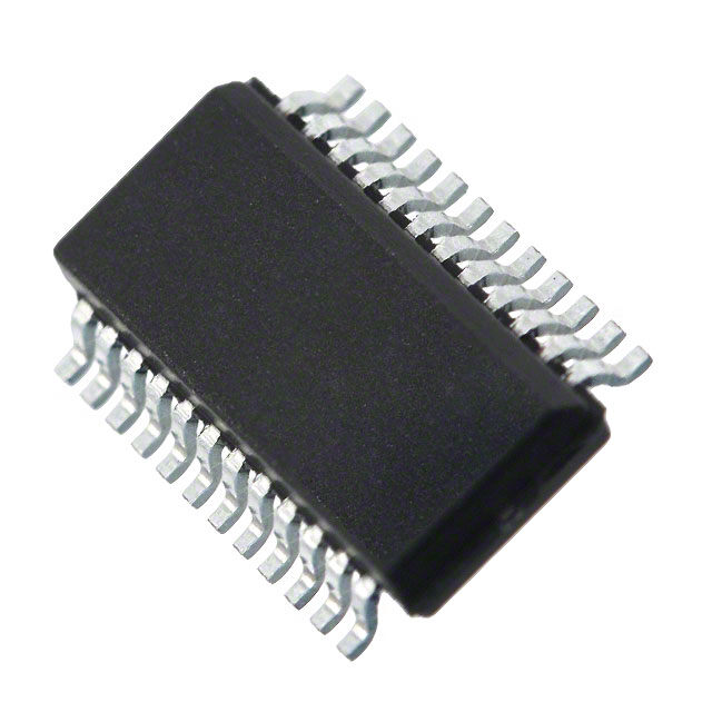
| 供应商器件封装 | 24-SSOP |
| 其它名称 | AS1113BSSU |
| 内部驱动器 | 是 |
| 包装 | 管件 |
| 商标 | ams |
| 安装类型 | 表面贴装 |
| 安装风格 | SMD/SMT |
| 封装 | Tube |
| 封装/外壳 | 24-SSOP(0.154",3.90mm 宽) |
| 封装/箱体 | SSOP-24 |
| 工作温度 | -40°C ~ 85°C |
| 工作电源电压 | 3 V to 5.5 V |
| 工厂包装数量 | 56 |
| 恒压 | - |
| 恒流 | 是 |
| 拓扑 | 16 位移位寄存器,PWM |
| 最大工作温度 | + 85 C |
| 最大电源电流 | 50 mA |
| 最小工作温度 | - 40 C |
| 标准包装 | 56 |
| 片段数量 | 16 |
| 电压-电源 | 3 V ~ 5.5 V |
| 电压-输出 | 15V |
| 类型-初级 | LED 照明显示器,标牌,汽车 |
| 类型-次级 | - |
| 输出数 | 16 |
| 频率 | 50MHz |
| 高电平输出电流 | 50 mA |


_renders/IS31FL3728-QFLS2-TR.jpg)

- 商务部:美国ITC正式对集成电路等产品启动337调查
- 曝三星4nm工艺存在良率问题 高通将骁龙8 Gen1或转产台积电
- 太阳诱电将投资9.5亿元在常州建新厂生产MLCC 预计2023年完工
- 英特尔发布欧洲新工厂建设计划 深化IDM 2.0 战略
- 台积电先进制程称霸业界 有大客户加持明年业绩稳了
- 达到5530亿美元!SIA预计今年全球半导体销售额将创下新高
- 英特尔拟将自动驾驶子公司Mobileye上市 估值或超500亿美元
- 三星加码芯片和SET,合并消费电子和移动部门,撤换高东真等 CEO
- 三星电子宣布重大人事变动 还合并消费电子和移动部门
- 海关总署:前11个月进口集成电路产品价值2.52万亿元 增长14.8%


PDF Datasheet 数据手册内容提取
austriamicrosystems AG is now ams AG The technical content of this austriamicrosystems datasheet is still valid. Contact information: Headquarters: ams AG Tobelbaderstrasse 30 8141 Unterpremstaetten, Austria Tel: +43 (0) 3136 500 0 e-Mail: ams_sales@ams.com Please visit our website at www.ams.com
Datasheet AS1113 50mA, 16-Channel LED Driver with Diagnostics 1 General Description 2 Key Features d The AS1113 is designed to drive up to 16 LEDs through ! 16 Constant-Current Output Channels a fast serial interface and features 16 output constant current drivers and an on-chip diagnostic read-back ! Excellent Output Current Accuracy i function. - Between Channels: <±3% l - Between Devices: <±6% a The high clock-frequency (up to 50MHz), adjustable out- put current, and flexible serial interface makes the ! Output Current Per Channel: 0.5 to 50mA v device perfectly suited for high-volume transmission applications. ! Controlled In-Rush Current Output current is adjustable (up to 50mA/channel) using ! Over-Temperature, Open-LED, Shorlted-LED an external resistor (REXT). Diagnostic Functions l i The serial interface with Schmitt trigger inputs includes ! LowG-Current Test Mode t an integrated shift register. Additionally, an internal data register stores the currently displayed data. ! Global Fault Monitoring s The device features integrated diagnostics for over- A! Low Shutdown Mod e Current: 10µA temperature, open-LED, and shorted-LED conditions. t Integrated registers store global fault status information ! Fast Serial Interface: 50MHz n during load as well as the detailed temperature/opens- ! Cascaded Configuration LED/shorted-LED diagnostics results. ! Extremeely Fast Output Drivers Suitable for PWM The AS1113 also features a low-current diagnomstic mode to minimize display flicker during fault testing. ! 24t-pin SSOP and 28-pin QFN (5x5mm) Package The AS1113 is available in a 24-pin SSOP and the 28- n pin QFN (5x5mm) package. a 3 Applications If a higher output current is needed, please see the o AS1110 with 100mA drive capability. The device is ideal for fixed- or slow-rolling displays c using static or multiplexed LED matrix and dimming functions, large LED matrix displays, mixed LED display and switch monitoring, displays in elevators, public l transports (underground, trains, buses, taxis, airplanes, a etc.), large displays in stadiums and public areas, price indicators in retail stores, promotional panels, bar-graph c displays, industrial controller displays, white good pan- els, emergency light indicators, and traffic signs. Figure 1. Main Diagram and Piin Assignments n +VLED OUTN0 cOUTN1 hOUTN2 OUTN3 OUTN4 OUTN5 OUTN6 OUTN7 OUTN8 OUTN9 OUTN10 OUTN11 OUTN12 OUTN13 OUTN14 OUTN15 e AS1113 T SDI SDO CLK LD OEN REXT GND VDD www.austriamicrosystems.com/LED-Driver-ICs/AS1113 Revision 1.04 1 - 24
AS1113 Datasheet Contents 1 General Description ................................................................................................................................ 1 2 Key Features .......................................................................................................................................... 1 3 Applications ............................................................................................................................................ 1 4 Pinout ..................................................................................................................................................... 3 d Pin Assignments ..................................................................................................................................................... 3 i Pin Descriptions ..................................................................................................................................................... 3 l 5 Absolute Maximum Ratings ....................................................................................................................a 4 6 Electrical Characteristics ........................................................................................................................ 5 v Switching Characteristics ....................................................................................................................................... 6 7 Typical Operating Characteristics ........................................................................................... ................ 7 l 8 Detailed Description ............................................................................................................................... 8 l Serial Interface .................................................................................. ......................................i............................... 9 Timing Diagrams ...........................................................................G......................................t................................... 9 Error-Detection Mode ....................................................................................................s....................................... 11 Global Error Mode ............................................................A..................................... ............................................... 11 Error Detection Functions ..................................................................................t................................................... 12 Open-LED Detection ...................................... ......................................n......................................................... 12 Shorted-LED ..............................................s................................................................................................... 12 Overtemperature .........................................................................e.................................................................. 12 m Detailed Error Reports .......................................................................................................................................... 13 t Detailed Temperature Warning Report ......................................................................................................... 13 n Detailed Open-LED Error Reaport .................................................................................................................. 14 Detailed Shorted-LED Error Report .............................................................................................................. 15 o Low-Current Diagnostic Mode ....................................................................................................................... 15 Shutdown Mode .................................................c................................................................................................... 16 9 Application Information ......................................................................................................................... 17 Error Detection .....................................l................................................................................................................ 17 Error Detection On-The-Fly .......a.................................................................................................................... 17 Error Detection with Low-Current Diagnosis Mode ....................................................................................... 17 c Cascading Devices ............................................................................................................................................... 18 Constant Current ............i...................................................................................................................................... 19 Adjusting Output Currennt ...................................................................................................................................... 19 Package Power Dissipation .................................................................................................................................. 19 h Delayed Outputs ................................................................................................................................................... 19 Switching-Noise Reduction .................................................................................................................................. 19 c Load Supply Voltage ............................................................................................................................................. 19 10 Packaege Drawings and Markings ....................................................................................................... 21 11 Ordering Information ........................................................................................................................... 23 T www.austriamicrosystems.com/LED-Driver-ICs/AS1113 Revision 1.04 2 - 24
AS1113 Datasheet - Pinout 4 Pinout Pin Assignments Figure 2. Pin Assignments (Top View) d SDI GND GND GND GND VDD REXT i 5 4 3 2 1 0 28 27 26 25 24 23 22 T N1 N1 N1 N1 N1 N1 N9 N8 l CLK 1 21 SDO DD EX DO EN UT UT UT UT UT UT UT UT a V R S O O O O O O O O O LD 2 20 OEN 24 23 22 21 20 19 18 17 16 15 14 13 v OUTN0 3 AS1113 19 OUTN15 OUTN1 4 28-pin QFN 5x5 18 OUTN14 AS1113 OUTN2 5 17 OUTN13 l 24-pin SSOP l OUTN3 6 16 OUTN12 i OUTN4 7 15 OUTN11 G 1 2 3 4 5 6 7 t8 9 10 11 12 8 9 10 11 12 13 14 GND SDI CLK LD TN0 TN1sTN2 TN3 TN4 TN5 TN6 TN7 OUTN5 OUTN6 OUTN7 N/C OUTN8 OUTN9 OUTN10 A t OU OU OU OU OU OU OU OU n s Pin Descriptions e Table 1. Pin Descriptions m t Pin Number Pin Name n Description SSOP QFN a 1 24:27 GND Ground o 2 28 SDI Serial Data Input c Serial Data Clock. The rising edge of the CLK signal is used to clock data 3 1 CLK into and out of the AS1113 shift register. In error mode, the rising edge of the CLK signal is used to switch error modes. l 4 2 LD Saerial Data Load Output Current Drivers. These pins are used as LED drivers or for input 3:10 c 5:20 OUTN0:15 sense for diagnostic modes. Data is transferred to the data register at the 12:19 rising edge of these pins. i Output Enable. The active-low pin OEN signal can always enable output n drivers to sink current independent of the AS1113 mode. 21 20 OEN 0 = Output drivers are enabled. h 1 = Output drivers are disabled. c Serial Data Output. In normal mode SDO is latched out 8.5 clock cycles after SDI is latched in. e In global error detection mode this pin indicates the occurrence of a global 22 21 SDO error. T 0 = Global error mode returned an error. 1 = No errors. External Resistor Connection. This pin connects through the external 23 22 REXT resistor (REXT) to GND, to setup the load current. 24 23 VDD Positive Supply Voltage - 11 N/C Not connected www.austriamicrosystems.com/LED-Driver-ICs/AS1113 Revision 1.04 3 - 24
AS1113 Datasheet - Absolute Maximum Ratings 5 Absolute Maximum Ratings Stresses beyond those listed in Table 2 may cause permanent damage to the device. These are stress ratings only, and functional operation of the device at these or any other conditions beyond those indicated in Section 6 Electrical Characteristics on page 5 is not implied. Exposure to absolute maximum rating conditions for extended periods may affect device reliability. d Table 2. Absolute Maximum Ratings Parameter Min Max Units Comments i VDD to GND 0 7 V l a Input Voltage -0.4 VDD V +0.4 v Output Voltage -0.4 15 V GND Pin Current 1000 mA l 88 ºC/W on PCB, 24-pin SSOP package l Thermal Resistance ΘJA 23 ºC/W on PCB, 28-pin QFN (5ix5mm) package Ambient Temperature -40 +85 ºC G t s Storage Temperature -55 150 ºC Humidity 5 86 A% Non-condensing t Electrostatic Digital Outputs 2 Discharge All Other Pins 2 kV Nnorm: MIL 833 E method 3015 s Latch-Up Immunity -100 - +100 + mA e EIA/JESD78 (INOM x m0.5) INOM tThe reflow peak soldering temperature (body temperature) specified is in accordance with n IPC/JEDEC J-STD-020D “Moisture/Reflow a Package Body Temperature +260 ºC Sensitivity Classification for Non-Hermetic Solid o State Surface Mount Devices”. The lead finish for Pb-free leaded packages is matte tin (100% Sn). c l a c i n h c e T www.austriamicrosystems.com/LED-Driver-ICs/AS1113 Revision 1.04 4 - 24
AS1113 Datasheet - Electrical Characteristics 6 Electrical Characteristics VDD = +3.0V to +5.5V, TAMB = -40°C to +85ºC (unless otherwise specified). Table 3. Electrical Characteristics Symbol Parameter Condition Min Typ Max Unit VDD Supply Voltage 3.0 5.5 V d VDS Output Voltage OUTN0:15 0 15.0 V i IOUT OUTN0:15 0.5 50 l IOH Output Current SDO -1.0 mAa IOL SDO 1.0 v VIH High Level 0.7 x VDD + VDD 0.3 Input Voltage CLK, OEN, LD, SDI V l0.3 x VIL Low Level -0.3 lVDD IDS(OFF) Output Leakage Current OEN = 1, VDS = 15.0V i 0.5 µA G t VOL IOL = +1.0mA s 0.4 Output SDO V VOH Voltage AIOH = -1.0mA V0D.4DV - t IAV(LC1) Device-to-Device Average Output VDS = 0.5V, VDD = Const., 25.25 mA Current from OUTN0 to OUTN15 REXT = 744Ω n ΔIAV(LC1) (BeCtwuererenn Ct Shkaenwne ls) sVDS ≥ R0.E5XVT, =V D7D4e 4=Ω C onst., ±1.5 ±3 % m IAV(LC2) Device-to-Device Average Output VDS = 0.6tV, VDD > 3.3V, 50.5 mA Current from OUTN0 to OUTN15 REXT = 372Ω n ΔIAV(LC2) Current Skew a VDS ≥ 0.6V, VDD = Const., ±1.5 ±3 % (Between Channels) REXT = 372Ω o ILC Low-Current Diagnosis Mode VDS = 0.8V, VDD = 5.0V 0.4 0.6 0.8 mA IPD Power Down Supply Current c VDS = 0.8V, VDD = 5.0V, 10 20 µA REXT = 372Ω, OUTN0:15 = On Output Current vs. %/ΔVDS Output Voltage Regulation l VDS within 1.0 and 3.0V ±0.1 %/V a Output Current vs. %/ΔVDD Supply Voltage Regulation VDD within 3.0 and 5.0V ±1 %/V c RIN(UP) Pullup Resistance OEN 250 500 800 kΩ RIN(DOWN) Pulldown Riesistance LD 250 500 800 kΩ n VTHL Error Detection Threshold Voltage 0.25 0.3 0.45 V h VDD = 3.0V 1.2 1.3 1.4 VTHH Error Detection Threshold Voltage V VDD = 5.0V 2.0 2.2 2.4 c TOV1 Overtemperature Threshold Flag 150 ºC IDD(OFF)0e REXT = Open‚ OUTN0:15 = Off 2.7 6 IDD(OFF)1 Off REXT = 744Ω‚ OUTN0:15 = Off 4.3 8 T Supply IDD(OFF)2 Current REXT = 372Ω‚ OUTN0:15 = Off 5.4 9 mA IDD(ON)1 REXT = 744Ω‚ OUTN0:15 = On 6.2 11 On IDD(ON)2 REXT = 372Ω‚ OUTN0:15 = On 10.5 15 www.austriamicrosystems.com/LED-Driver-ICs/AS1113 Revision 1.04 5 - 24
AS1113 Datasheet - Electrical Characteristics Switching Characteristics VDD = 3.0 to 5.5V, VDS = 0.8V, VIH = VDD, VIL = GND, REXT = 372Ω, VLOAD = 4.0V, RLOAD = 64Ω, CLOAD = 10pF; guar- anteed by design. Table 4. Switching Characteristics for VDD = 5V Symbol Parameter Conditions Min Typ Max Unit tP1 CLK - SDO 5 10 d Propagation Delay Time (Without tP2 Staggered Output Delay) LD - OUTNn 100 200 ns tP3 OEN - OUTNn 100 200 i l tP4 Propagation Delay Time 10 ns a tW(CLK) CLK 15 tW(L) Pulse Width LD 15 vns tW(OE) OEN (@IOUT < 60mA) 200 tR * CLK Rise Time 500 ns l tF * CLK Fall Time l500 ns tOR Output Rise Time of VOUT (Turn Off) i100 200 ns tOF Output Fall Time of VOUT (Turn On) G t100 300 ns tSU(D) Setup Time for SDI s5 ns tH(D) Hold Time for SDI A 5 ns tSU(L) Setup Time for LD t 5 ns tH(L) Hold Time for LD 5 ns n tTESTING OEN Time for Error Detection 2000 ns s tSTAG Staggered Output Delay e 20 40 ns tSU(OE) Output Enable Setup Timme 20 ns tGSW(ERROR) Global Error Switching Setup Time t 10 ns tSU(ERROR) Global Error Detection Setup Time n 10 ns tP(I/O) Propagation Delay Glaobal Error Flag 5 ns tSW(ERROR) Switching Time Global Error Flag o 10 ns Maximum Clock Frequency fCLK (Cascade Operation) c 30 50 MHz tP3,ON Low-Current Test Mode Turn ON 3 5 µs tP3,OFF Propagation Delay Time Turn OFF 0.05 0.1 µs l Change from REXT1 = 372Ω, tREXT2,1 External Resistor Reacation Time IOUT1 = 50.52mA to REXT2 = 0.5 1 µs 37.2kΩ, IOUT2 < 1mA c Change from REXT1 = 37.2kΩ, tREXT2,1 External Resistor Reaction Time IOUT1 = 0.5mA to REXT2 = 0.5 1 µs i 372Ω, IOUT2 > 25mA * If multiple AS1113 devicesn are cascaded and tr or tf is large, it may be critical to achieve the timing required for data transfer between two cascaded LED drivers. h c e T www.austriamicrosystems.com/LED-Driver-ICs/AS1113 Revision 1.04 6 - 24
AS1113 Datasheet - Typical Operating Characteristics 7 Typical Operating Characteristics Figure 3. Output Current vs. REXT, Figure 4. Relative Output Current Error vs. VDD, VDD = 5V; VDS = 0.8V, TAMB = 25°C Iout/Iout@VDD=5V - 1, TAMB = 25°C 100 2 ) % 1.5 r ( d o rr 1 E UT (mA) . 10 ut Current .0.50 RVDESX T= =0 .754V4Ω; ali IO utp -0.5 REXT = 372Ω; v O VDS = 0.6V e -1 v ati -1.5 l el l R 1 -2 i 100 1000 10000 3G 3.5 4 4.5t5 5.5 REXT ( Ω ) VDD (sV) Figure 5. Output Current vs. VDS; FigAure 6. Output Current vs. VDS; VDD = 5V, TAMB = 25°C VDD = 5V, TAMB = 25°C t 60 60 n s 50 50 e REXT = 376Ω REXT = 376Ω m 40 40 t A) . REXT = 470Ω A) . n REXT = 470Ω m 30 a m 30 (UT REXT = 627Ω o (UT REXT = 627Ω O O I 20 I 20 REXT = 940Ω REXT = 940Ω c 10 10 l 0 0 a 0 3 6 9 12 15 0 0.2 0.4 0.6 0.8 1 1.2 V (V) V (V) DS c DS i n h c e T www.austriamicrosystems.com/LED-Driver-ICs/AS1113 Revision 1.04 7 - 24
AS1113 Datasheet - Detailed Description 8 Detailed Description The AS1113 is designed to drive up to 16 LEDs through a fast serial interface and 16 constant-current output drivers. Furthermore, the AS1113 provides diagnostics for detecting open- or shorted-LEDs, as well as over-temperature con- ditions for LED display systems, especially LED traffic sign applications. The AS1113 contains an 16-bit shift register and an 16-bit data register, which convert serial input data into parallel out- d put format. At AS1113 output stages, sixteen regulated current sinks are designed to provide uniform and constant cur- rent with excellent matching between ports for driving LEDs within a wide range of forward voltage variations. External output current is adjustable from 0.5 to 50mA using an external resistor for flexibility in controlling the brightness inten- i sity of LEDs. The AS1113 guarantees to endure 15V maximum at the outputs. l a The serial interface is capable of operating at a minimum of 30 MHz, satisfying the requirements of high-volume data transmission. v Using a multiplexed input/output technique, the AS1113 adds additional functionality to pins SDO, LD and OEN. These pins provide highly useful functions (open- and shorted-LED detection, over-temperature detection), thus reducing pin count. Over-temperature detection will work on-the-run, whereas the open- and shorted-LED detectionl can be used on-the-run or in low-current diagnostic mode (see page 15). l i Figure 7. AS1113 - Block Diagram G t s +VLED 0 1 2 3 4 5 6 7 8 A9 10 11 12 13 14 15 N N N N N N N N N N N N N N N N T T T T T T T T T T T T tT T T T U U U U U U U U U U U U U U U U O O O O O O O O O O O O O O O O n s e m t Temperature 16-Bit Open 16-Bit Short AS1113 Dentection & Detection & Detection REXT a Error Register Error Register Current o Generators OEN c LD 16-Bit Data Register lDetailed Error Global a Detection Error Detection c CLK 16-Bit Shift Reigister SDI n Control Logic h SDO c e T Indicates 16 Bit Path www.austriamicrosystems.com/LED-Driver-ICs/AS1113 Revision 1.04 8 - 24
AS1113 Datasheet - Detailed Description Serial Interface Data accesses are made serially via pins SDI and SDO. At each CLK rising edge, the signal present at pin SDI is shifted into the first bit of the internal shift register and the other bits are shifted ahead of the first bit. The MSB is the first bit to be clocked in. In error-detection mode the shift register will latch-in the corresponding error data of tempera- ture-, open-, and short-error register with each falling edge of LD. The 16-bit data register will latch the data of the shift register at each rising edge of LD. This data is then used to drive d the current generator output drivers to switch on the corresponding LEDs as OEN goes low. i Timing Diagrams l This section contains timing diagrams referenced in other sections of this data sheet. a Figure 8. Normal Mode Timing Diagram v tW(CLK) l CLK 50% 50% 50% l i tSU(D) tH(D) G t s SDI 50% 50% A t SDO 50% n s tP1 e m tW(L) t LD 50% n50% a tSU(L) tH(L) o OEN OENc Low = Output Enabled OUTNx High = Output Off OUTNx 50% l OUTNx Low = Output On a tP2 c Figure 9. Output Delay Timing Diagram i n tW(OE) h OEN 50% 50% c tP3 tP3 90% 90% OUTeN0 50% 10% 10% 50% tOF tOR T tSTAG tSTAG OUTN1 50% 50% 14XtSTAG 14XtSTAG 50% 50% OUTN15 www.austriamicrosystems.com/LED-Driver-ICs/AS1113 Revision 1.04 9 - 24
AS1113 Datasheet - Detailed Description Figure 10. Data Input Timing Diagram OEN tW(OE) tSU(L) tSU(OE) d LD 16 CLK Pulses tW(L) i l a CLK v tSU(D) Data Bit Data Bit Data Bit Data Bit Data Bit Data Bit Data Bit Data Bit l SDI0 Don’t Care 15 14 13 12 n 2 1 0 l i G tH(D) t s SDO0 Old Data Old Data Old Data Old Data Old Data Old Data Old Data Old Data Don’t Care Bit 15 Bit 14 Bit 13 Bit 12 Bit n Bit 2 Bit 1 Bit 0 A tP1 t n Figure 11. Data Input Example Timing Diagram s e m t Time 1 2 3 4 5 6 7 8 9 10 11 12 13 14 15 CLK n a SDI D1 D14 D13 D12 D11 D10 D9 D8 D7 D6 D5 D4 D3 D2 D1 D0 o LD OEN c OUTN0 Off On OUTN1 Off l On OUTN2 a Off On OUTN3 Off c On OUTN4 Off On OUTN5 i Off On OUTN6 n Off On OUTN7 Off h On OUTN8 Off On OUTN9 c Off On OUTN10 Off e On OUTN11 Off On OUTTN12 Off On OUTN13 Off On OUTN14 Off On OUTN15 Off On www.austriamicrosystems.com/LED-Driver-ICs/AS1113 Revision 1.04 10 - 24
AS1113 Datasheet - Detailed Description Figure 12. Switching Global Error Mode Timing Diagram OEN tTESTING tGSW(ERROR) LD tSU(ERROR) tGSW(ERROR) d tP(I/O) tP(I/O) tP(I/O) i l CLK tGSW(ERROR) a v SDI TFLAG(IN) OFLAG(IN) SFLAG(IN ) l l i SDO DCoanre’t TFLAG G DCoanre’t OFLAG tDCoanre’t SFLAG s Acquisition of tP4 tSW(EARROR) tSW(ERROR) Error Status t n Error-Detection Mode s e Acquisition of the error status occurs at the rising edge of OEN. Error-detection mode is started on the rising edge of m LD when OEN is high. The CLK signal must be low when entering error detection mode. Error detection for open- and t shorted-LEDs can only be performed for LEDs that are switched on during test time. To switch between error-detection modes clock pulses are needed (see Table 5). n a Note: To test all LEDs, a test pattern that turns on all LEDs must be input to the AS1113. o Global Error Mode c Global error mode is entered when error-detection mode is started. Clock pulses during this period are used to select between temperature, open-LED, and shorted-LED tests, as well as low-current diagnostic mode and shutdown mode (see Table 5). In global error mode, an error flag (TFLAG, OFLAG, SFLAG) is delivered to pin SDO if any errors are l encountered. a Table 5. Global Error Mode Selections c Clock Output Port Error-Detection Mode Global Error Flag/Shutdown Condition Pulses i 0 Don't Care nOver-Temperature TFLAG = SDO = 1: No over-temperature warning. Detection TFLAG = SDO = 0: Over-temperature warning. 1 Enabled h Open-LED Detection OFLAG = SDO = 1: No open-LED error. OFLAG = SDO = 0: Open-LED error. c SFLAG = SDO = 1: No shorted-LED error. 2 Enabled Shorted-LED Detection SFLAG = SDO = 0: Shorted-LED error. e Low-Current Diagnostic 3 Don't Care Mode T SDI = 1: Wakeup 4 Don't Care Shutdown Mode SDI = 0: Shutdown Note: For a valid result SDI must be 1 for the first device. www.austriamicrosystems.com/LED-Driver-ICs/AS1113 Revision 1.04 11 - 24
AS1113 Datasheet - Detailed Description If there are multiple AS1113s in a chain, the error flag will be gated through all devices. To get a valid result at the end of the chain, a logic 1 must be applied to the SDI input of the first device of the chain. If one device produces an error this error will show up after n*tP(I/O) + tSW(ERROR) at pin SDO of the last device in the chain. This means it is not possi- ble to identify which device in the chain produced the error. Therefore, if a global error occurs, the detailed error report can be run to identify which AS1113, or LED produced the error. Note: When no error has occurred, the detailed error report can be skipped, setting LD and subsequently OEN low. d Error Detection Functions i Open-LED Detection l The AS1113 open-LED detection is based on the comparison between VDS and VTHL. The open LED status is aquiread at the rising edge of OEN and stored internally. While detecting open-LEDs the output port must be turned on. Open LED detection can be started with 1 clock pulse during error detection mode while the output port is turned on.v Note: LEDs which are turned off at test time cannot be tested and will be shown as a logic 1 in the deta iled error report. l l Table 6. Open LED Detection Modes i Output Port State Effective Output DeteGcted Open-LED t Meaning Point Conditions Error Status Code s On VDS < VTHL 0 Open Circuit On VDS > VTHL A 1 Normal t Shorted-LED n The AS1113 shorted-LED detection is based on the csomparison between VDS and VTHH. The shortened LED status is aquired at the rising edge of OEN and stored internally. While detecting sehorted-LEDs the output port must be turned on. Shorted-LED detection can be started with m2 clock pulses during error detection mode while the output port is turned on. t For valid results, the voltage at OUTN0:OUTN15 must be lower tnhen VTHH under low-current diagnostic mode operat- ing conditions. This can be achieved bay reducing the VLED voltage or by adding additional diodes, resistors or LED’s. o Note: LEDs which are turned off at test time cannot be tested and will be shown as a logic 1 in the detailed error report. c Table 7. Shorted LED Detection Modes Effective Output Detected Shorted-LED Output Port State l Meaning Point Conditions Error Status Code a On VDS > VTHH 0 Short Circuit On cVDS < VTHH 1 Normal Overtemperature i Thermal protection for the AnS1113 is provided by continuously monitoring the device’s core temperature. The overtem- perature status is aquired at the rising edge of OEN and stored internally. Table 8. Overtemperahture Modes Effective Output Detected Overtemperature Output Port State Meaning c Point Conditions Status Code Overtemperature Doen’t Care Temperature > TOV1 0 Condition Don’t Care Temperature < TOV1 1 Normal T www.austriamicrosystems.com/LED-Driver-ICs/AS1113 Revision 1.04 12 - 24
AS1113 Datasheet - Detailed Description Detailed Error Reports The detailed error report can be read out after global error mode has been run. At the falling edge of LD, the detailed error report of the selected test is latched into the shift register and can be clocked out with n*16 clock cycles (n is the number of AS1113s in a chain) via pin SDO. At the same time new data can be written into the shift register, which is loaded on the next rising edge of pin LD. This pattern is shown at the output drivers, at the falling edge of OEN. Detailed Temperature Warning Report d The detailed temperature warning report can be read out immediately after global error mode has been run. SDI must i be 1 for the first device. Bit0 of the 16bit data word represents the temperature flag of the chip. l Figure 13. Detailed Temperature Warning Report Timing Diagram a v Global Flag Readout Detailed Error Report Readout OEN l tH(L) tGSW(ERROR) l LD i G t t(SU)ERROR tP4 s CLK A t Don’t SDI DBit15 DBit14 DBit13 DBit12 DBitn DBit2 DBit1 DBit0 n Care s New Data Input SDO TFLAG Undefineed TBit0 Don’t Care m tP4 Temperature Errtor Report Output tP1 For detailed timing information see Timing Diagrams on page 9. n a Detailed Temperature Warning Report Example o Consider a case where four AS1113s are cascaded in one chain. The detailed error report lists the temperatures for each device in the chain: c IC1:[70°] IC2:[85°] IC3:[170°] IC4:[60°] In this case, IC3 is overheated and will generate a global error, and therefore 4*16 clock cycles are needed to write out l the detailed temperature warning report, and optionally read in new data. The detailed temperature warning report a would look like this: XXXXXXXXXXXXXXX1 XcXXXXXXXXXXXXXX1 XXXXXXXXXXXXXXX0 XXXXXXXXXXXXXXX1 The 0 in the detailed temperature warning report indicates that IC3 is the device with the over-temperature condition. i Note: In an actual report thnere are no spaces in the output. h c e T www.austriamicrosystems.com/LED-Driver-ICs/AS1113 Revision 1.04 13 - 24
AS1113 Datasheet - Detailed Description Detailed Open-LED Error Report The detailed open-LED error report can be read out immediately after global error mode has been run. SDI must be 1 for the first device. Figure 14. Detailed Open-LED Error Report Timing Diagram Global Flag Readout Detailed Error Report Readout d OEN i tTESTING l tH(L) a LD tSU(ERROR) v tGSW(ERROR) tP4 tGSW(ERROR) CLK l l tGSW(ERROR) i Don’t SDI Acquisition of Error Status tSW(ERROR) DBit15 DBit14 DBiNt1e3wDG BDita1t2a IDnBpitunt DBit2 DBit1 DsBit0tCare A Don’t SDO TFlag OFlag OBit15 OBit14 OBit13 OBit12 OBitn OBtit2 OBit1 OBit0 Care tP4 Open Error Report Outpunt tP1 For detailed timing information see Timing Diagrams on page 9. s e Detailed Open-LED Error Report Example m Consider a case where three AS1113s are cascaded in one chain. At 1 indicates a LED is on, a 0 indicates a LED is off, and an X indicates an open LED. The open-LED test is only applied to LEDs that are turned on. This test is used with n a test pattern where all LEDs are on at test time. a IC1:[1111111111111111] IC2:[111XX11111111X11] IC3:[1111o111111111111] IC2 has three open LEDs switched on due to input. 3*16 clock cycles are needed to write the entire error code out. The detailed error report would look like this: c Input Data: 111111111111111 1 1111111111111111 1111111111111111 l LED Status: 1111111111111111 111XX11111111X11 1111111111111111 a Failure Code: 1111111111111111 1110011111111011 1111111111111111 c Comparing this report with the input data indicates that IC2 is the device with two open LEDs at position 4 and 5 and one open LED at position 14. For such a test it is recommended to enter low-current diagnostic mode first (see Low- i Current Diagnostic Mode on page 15) to reduce screen flickering. n This test can be used also on-the-fly without using an all 1s test pattern (see Figure 18 on page 17). h Note: In an actual report there are no spaces in the output. LEDs turned off during test time cannot be tested and will show a logic 1 in the detailed error report. c e T www.austriamicrosystems.com/LED-Driver-ICs/AS1113 Revision 1.04 14 - 24
AS1113 Datasheet - Detailed Description Detailed Shorted-LED Error Report The detailed shorted-LED error report can be read out immediately after global error mode has been run (see Global Error Mode on page 11). SDI must be 1 for the first device. Figure 15. Detailed Shorted-LED Error Report Timing Diagram GGlloobbaall FFllaagg RReeaaddoouutt Detailed Error Report Readout d OEN i tTESTING l a LD tSU(ERROR) tH(L) v tGSW(ERROR) tP4 CLK tGSW(ERROR) l l tGSW(ERROR) i SDI Acquisition of Error Status tSW(ERROR) DBit15 DBit14 DBit1N3eDwGB iDt12ata DInBpitnut DBit2 DBit1 sDBit0t DCoanre’t SDO TTFFLLAAGGOFLAG SFLAG SBit15 SBitA14 SBit13 SBit12 SBitn SBit2 SBit1 SBit0 DCoanre’t t tP4 Shorted-LED Error Repornt Output tP1 For detailed timing information see Timing Diagrams on page 9. s e Detailed Shorted-LED Error Report Example m t Consider a case where three AS1113s are cascaded in one chain. A 1 indicates a LED is on, a 0 indicates a LED is off, and an X indicates a shorted LED. This test is used on-the-fly. n a IC1:[11111XX111111111] IC2:[1111111111111111] IC3:[X100011111111111] o IC1 has two shorted LEDs which are switched on, IC3 has one shorted LED switched off due to input. 3*16 clock cycles are needed to write the entire error code out. cThe detailed error report would look like this: Input Data: 111111111111111 1 1111111111111111 0100011111111111 LED Status: 11111XX111111l111 1111111111111111 X111111111111111 a Failure Code: 1111100111111111 1111111111111111 1111111111111111 c Showing IC1 as the device with two shorted LEDs at position 6 and 7, and IC3 with one shorted LED at position 1. The shorted LED at position 1 of IC3 cannot be detected, since LEDs turned off at test time are not tested and will show a i logic "1" at the detailed error report. To test all LEDs this test should be run with an all 1s test pattern. For a test with an n all on test pattern, low-current diagnostic mode should be entered first to reduce on-screen flickering. Note: In an actual rehport there are no spaces in the output. LEDs turned off during test time cannot be tested and will show a logic 1 in the detailed error report. c Low-Current Diagnostic Mode To run the eopen- or shorted-LED test, a test pattern must be used that will turn on each LED to be tested. This test pat- tern will cause a short flicker on the screen while the test is being performed. The low-current diagnostic mode can be initiaTted prior to running a detailed error report to reduce this on-screen flickering. Note: Normally, displays using such a diagnostic mode require additional cables, resistors, and other components to reduce the current. The AS1113 has this current-reduction capability built-in, thereby minimizing the number of external components required. Low-current diagnostic mode can be initiated via 3 clock pulses during error-detection mode. After the falling edge of LD, a test pattern displaying all 1s can be written to the shift register which will be used for the next error-detection test. www.austriamicrosystems.com/LED-Driver-ICs/AS1113 Revision 1.04 15 - 24
AS1113 Datasheet - Detailed Description On the next falling edge of OEN, current is reduced to ILC. With the next rising edge of OEN the current will immedi- ately increase to normal levels and the detailed error report can be read out entering error-detection mode. Figure 16. Switching into Low-Current Diagnostic Mode Timing Diagram Low-Current Diagnosis Mode OEN d tTESTING tSU(ERROR) Load Internal all 1s i LD Test Pattern l (optional) a tGSW(ERROR) tH(L) v CLK tGSW(ERROR) l tSW(ERROR) l SDI Re-entering Error Detectioin Mode G (see tFigure 14) SDO TFLAG OFLAG SFLAG DCoanre’t (ssee Figure 15) tP1 A Normal Operation Current For detailed timing information see Timing Diagrams on page 9. t Shutdown Mode n s The AS1113 features a shutdown mode which can be entered via 4 clock pulses during error-detection mode. To e enable the shutdown mode a 0 must be placed at SDI after the rising edge of the 3rd clock pulse. m To disable shutdown mode a 1 must be placed at SDI after the 3rd ctlock pulse. The shutdown/wakeup information will be latched through if multiple AS1113 devices are in a chain. At tnhe rising edge of the 4th clock pulse the shutdown bit will be read out and the AS1113 will shautdown or wakeup. o Note: In shutdown mode the supply current drops down to <10µA. Figure 17. Shutdown Mode Timing Diagram c l OEN a c LD tSU(ERROR)i n h CLK c 1 = Wakeup e SDI 0 = Shutdown T 1 = Wakeup SDO TFLAG OFLAG SFLAG 0 = Shutdown tP4 tSU(D) www.austriamicrosystems.com/LED-Driver-ICs/AS1113 Revision 1.04 16 - 24
AS1113 Datasheet - Application Information 9 Application Information Error Detection The AS1113 features two types of error detection. The error detection can be used on-the-fly, for active LEDs, without any delay, or by entering into low-current diagnosis mode. d Error Detection On-The-Fly Error detection on-the-fly will output the status of active LEDs during operation. Without choosing an error mode this i will output the temperature flag at every input/output cycle. Triggering one clock pulse for open or two clock pulses for l short detection during error detection mode outputs the detailed open- or short-error report with the next input/outpuat cycle (see Figure 18). LEDs turned off at test time are not tested and will show a logic "1" at the detailed error report. v Figure 18. Normal Operation with Error Detection During Operation – 64 Cascaded AS1113s Display Data1 Data2 Data3l l i SDI Data2 Data3 G tData4 s T/O or S Error Code T/O or S Error Code T/O or S Error Code SDO GEF GEF Data0 DatAa1 Data2 Clock for Error Clock for Errotr Mode 0x/1x/2x Mode 0x/1x/2x CLK 1024x 1024x n 1024x s Rising Edge of OEN Rising Edge of OeEN OEN Acquisition of Error Status m Acquisition of Error Status t Falling Edge of LD; Error Register is Falling Edge of LD; Error Register is LD copied into Shift Regnister copied into Shift Register a Current o≤ 50mA GEF = Global Error Flag c Error Detection with Low-Current Diagnosis Mode This unique feature of the AS1113 uses an inlternal all 1s test pattern for a flicker free diagnosis of all LEDs. This error detection mode can be started at the end aof each input cycle (see Figure 19). Figure 19. Low-Current Diagnosis Mcode with Internal All 1s Test Pattern – 64 Cascaded AS1113s Low-Current Diagnosis Mode i Display Data0 Data1 Data2 n SDI Data1 Data2 Data3 h SDO T/cO or SD aEtarr0or Code GEF O oArl lS 1 sE rTreosr tC Poadttee rfrnom GEF Temperature Error Code 3x Clocks Low-Clock for Error e Current Mode Mode 1x/2x CLK 1024x 1024x 1024x T Rising Edge of OEN OEN Acquisition of Error Status Use Internal All 1s Falling Edge of LD; Error Register LD Test Pattern is copied into Shift Register Current ≤ 50mA ≤ 50mA ≤ 0.8mA GEF = Global Error Flag www.austriamicrosystems.com/LED-Driver-ICs/AS1113 Revision 1.04 17 - 24
AS1113 Datasheet - Application Information The last pattern written into the shift register will be saved before starting low-current diagnosis mode and can be dis- played immediately after the test has been performed. Low-current diagnostic mode is started with 3 clock pulses during error detection mode. Then OEN should be enabled for ≥2µs for testing. With the rising edge of OEN the LED test is stopped, and while LD is high the desired error mode can be selected with the corresponding clock pulses. After LD and OEN go low again the previously saved pattern can be displayed at the outputs. d With the next data input the detailed error code will be clocked out at pin SDO. Note: See Figure20 for use of an external test pattern. i l Figure 20. Low-Current Diagnosis Mode with External Test Pattern – 64 Cascaded AS1113s a Low-Current Diagnosis Mode v Display Data1 Data2 SDI External all 1s Test Pattern Data2 Datla3 l T/O or S Error Code O or S Error Co de i SDO Data0 GEF from Test PaGttern GEF Temtperature Error Code 3x Clocks Low-Current Clock for Error s Mode Mode 1x/2x CLK 1024x A 1024x 1024x t OEN Rising Edge of OEN Acquisit ion of Error Status n sFalling Edge of LD; Error Register LD is copied into Shift Regiseter m Current t ≤ 50mA ≤ 50mA n ≤ 0.8mA a GEF = Global Error Flag o Cascading Devices c To cascade multiple AS1113 devices, pin SDO must be connected to pin SDI of the next AS1113 (see Figure 21). At each rising edge of CLK the LSB of the shift register will be written into the shift register SDI of the next AS1113 in the l chain. a Note: When n*AS1113 devices are in one chain, n*16 clock pulses are needed to latch-in the input data. c Figure 21. Cascading AS1113 Devices i n h SDI c AS1113 #1 AS1113 #2 AS1113 #n-1 SDI SDO SDI SDO SDI SDO e T CLK LD OEN CLK LD OEN CLK LD OEN CLK LD OEN www.austriamicrosystems.com/LED-Driver-ICs/AS1113 Revision 1.04 18 - 24
AS1113 Datasheet - Application Information Constant Current In LED display applications, the AS1113 provides virtually no current variations from channel-to-channel and from AS1113-to-AS1113. This is mostly due to 2 factors: ! While IOUT ≥ 10mA, the maximum current skew is less than ±3% between channels and less than ±6% between AS1113 devices. ! In the saturation region, the characteristic curve of the output stage is flat (see Figure 5 on page 7). Thus, the out- d put current can be kept constant regardless of the variations of LED forward voltages (VF). i Adjusting Output Current l a The AS1113 scales up the reference current (IREF) set by external resistor (REXT) to sink a current (IOUT) at each out- put port. As shown in Figure3 on page7 the output current in the saturation region is extremely flat so that it is possi- v ble to define it as target current (IOUT TARGET). IOUT TARGET can be calculated by: VREXT = 1.253V (EQ 1) IREF = VREXT/REXT (if the other end of REXT is connected to ground) l (EQ 2) IOUT TARGET = IREF*15 = (1.253V/REXT)*15 l (EQ 3) Where: i G t REXT is the resistance of the external resistor connected to pin REXT. s VREXT is the voltage on pin REXT. The magnitude of current (as a function of REXT) is around 50.A52mA at 372Ω and 25. 26mA at 744Ω. Figure3 on page7 shows the relationship curve between the IOUT TARGET of each channel andt the corresponding external resistor (REXT). n s Package Power Dissipation e The maximum allowable package power dissipmation (PD) is determined as: t PD(MAX) = (TJ-TAMB)/RTH(J-A) (EQ 4) n When 16 output channels are turned on simultaneously, the actual package power dissipation is: a PD(ACT) = (IDD*VDD) + (IOUT*Duty*VDS*16) (EQ 5) o Therefore, to keep PD(ACT) ≤ PD(MAX), the maximum allowed output current as a function of duty cycle is: IOUT = {[(TJ-TAMB)/RTHc(J-A)]-(IDD*VDD)}/VDS/Duty/16 (EQ 6) Where: TJ = 150ºC l Delayed Outputs a The AS1113 has graduated delay circcuits between outputs. These delay circuits can be found between OUTNn and constant current block. The fixed delay time is 20 ns (tiyp) where OUTN0 has no delay, OUTN1 has 20ns delay, OUTN2 has 40ns delay ... OUTN15 has 300ns delay. Tnhis delay prevents large inrush currents, which reduce power supply bypass capacitor requirements when the outputs turn on (see Figure 10 on page 10) h Switching-Noise Reduction c LED drivers are frequently used in switch-mode applications which normally exhibit switching noise due to parasitic inductance on the PCB. e Load Supply Voltage T Considering the package power dissipation limits (see EQ 4:6), the AS1113 should be operated within the range of VDS = 0.4 to 1.0V. For example, if VLED is higher than 5V, VDS may be so high that PD(ACT) > PD(MAX) where VDS = VLED - VF. In this case, the lowest possible supply voltage or a voltage reducer (VDROP) should be used. The voltage reducer allows VDS = (VLED -VF) - VDROP. Note: Resistors or zener diodes can be used as a voltage reducer as shown in Figure22. www.austriamicrosystems.com/LED-Driver-ICs/AS1113 Revision 1.04 19 - 24
AS1113 Datasheet - Application Information Figure 22. Voltage Reducer using Resistor (Left) and Zener Diode (Right) Voltage Supply Voltage Supply { } VDROP VDROP VLED VLED VF VDS d VF VDS i l AS1113 a AS1113 v l l i G t s A t n s e m t n a o c l a c i n h c e T www.austriamicrosystems.com/LED-Driver-ICs/AS1113 Revision 1.04 20 - 24
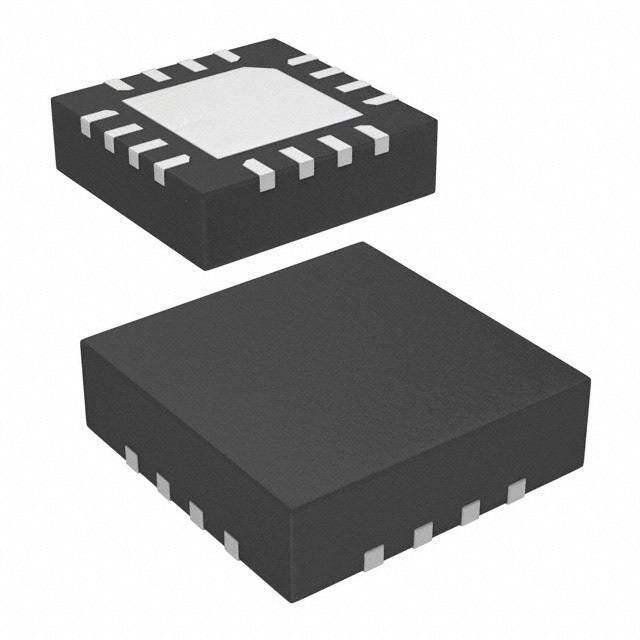
AS1113 Datasheet - Package Drawings and Markings 10 Package Drawings and Markings The AS1113 is available in a 28-pin QFN (5x5mm) package and a 24-pin SSOP package. Figure 23. 28-pin QFN (5x5mm) Packagee D -A- D2 d INDEX AREA D/2 D2/2 (D/2 xE/2) -B- i 4 l E/2 NXL 2/2 a e E v2 E E x -B- 2 C SEE 2 DETAIL B aa 1 l a l i aaa C2x IN(DD/2E Xx EA/2R)EA G N6N-1 -A- stNXbbbb 5 C A B TOP VIEW SEE ddd C 4 DETAIL B Datum A or B A BTM VIEW t n 1 ccc C L s A NX 0.08 C e SEATING m SIDE VIEW PLANE -C- e Terminal Tip tA1 A3 ODD TERMINAL SIDE 5 n a Symbol Min Typ Max Notes Symbol Min Typ Max Notes o A 0.70 0.75 0.80 1, 2 D BSC 5.00 1, 2 A1 0.00 0.02 0.05 1, 2 E BSC 5.00 1, 2 c A3 0.20 REF 1, 2 D2 3.00 3.15 3.25 1, 2 L 0.45 0.55 0.65 1, 2 E2 3.00 3.15 3.25 1, 2 L1 0.03 0.15 l1, 2 K 0.20 1, 2 a aaa 0.15 1, 2 b 0.18 0.25 0.30 1, 2, 5 bbb 0.10 1, 2 e 0.50 c ccc 0.10 1, 2 N 28 1, 2 ddd 0.05i 1, 2 ND 7 1, 2, 5 eee 0n.08 1, 2 NE 7 1, 2, 5 ggg 0.10 1, 2 h Notes:Unilateracl coplanarity zone applies to the exposed heat sink slug as well as the terminals. 1. Dimensioning and tolerancing conform to ASME Y14.5M-1994. e 2. All dimensions are in millimeters; angles in degrees. 3. NT is the total number of terminals. 4. The terminal #1 identifier and terminal numbering convention shall conform to JEDEC 95 SPP-012. Details of termi- nal #1 identifier are optional but must be located within the zone indicated. The terminal #1 identifier may be either a mold or marked feature. 5. Dimension b applies to metallized terminal and is measured between 0.15 and 0.30mm from terminal tip. If one end of the terminal has the optional radius, the b dimension should not be measured in that radius area. 6. Dimensions ND and NE refer to the number of terminals on each D and E side, respectively. www.austriamicrosystems.com/LED-Driver-ICs/AS1113 Revision 1.04 21 - 24
AS1113 Datasheet - Package Drawings and Markings Figure 24. 24-pin SSOP Package d i l a v l l i G t s A t n s e m t Symbol Min Max n A 1.35 1.75 a A1 0.10 0.25 o A2 1.37 1.57 b 0.20 0.30 c C 0.19 0.25 D 8.55 8.74 l E 5.79 6.20 a E1 3.81 3.99 e 0.635 BSC c h 0.22 0.49 i L 0.40 1.27 n θ 0º 8º h c e T www.austriamicrosystems.com/LED-Driver-ICs/AS1113 Revision 1.04 22 - 24
AS1113 Datasheet - Ordering Information 11 Ordering Information The device is available as the standard products shown in Table 9. Table 9. Ordering Information Ordering Code Description Delivery Form Package d AS1113-BSSU 50mA, 16-Channel LED Driver with Diagnostics Tubes 24-pin SSOP AS1113-BSST 50mA, 16-Channel LED Driver with Diagnostics Tape and Reel 24-pin SSOP i AS1113-BQFR 50mA, 16-Channel LED Driver with Diagnostics Tray 28-pin QFN (5x5mm) l a AS1113-BQFT 50mA, 16-Channel LED Driver with Diagnostics Tape and Reel 28-pin QFN (5x5mm) v Note: All products are RoHS compliant and Pb-free. Buy our products or get free samples online at ICdirect: http://www.austriamicrosystems.com/IlCdirect l For further information and requests, please contact us mailto:sa les@austriamicrosystemis.com or find your local distributor at http://www.austriamicrosystemsG.com/distributor t s A t n s e m t n a o c l a c i n h c e T www.austriamicrosystems.com/LED-Driver-ICs/AS1113 Revision 1.04 23 - 24
AS1113 Datasheet Copyrights Copyright © 1997-2009, austriamicrosystems AG, Tobelbaderstrasse 30, 8141 Unterpremstaetten, Austria-Europe. Trademarks Registered ®. All rights reserved. The material herein may not be reproduced, adapted, merged, translated, stored, or used without the prior written consent of the copyright owner. All products and companies mentioned are trademarks or registered trademarks of their respective companies. d Disclaimer i l Devices sold by austriamicrosystems AG are covered by the warranty and patent indemnification provisions appearing a in its Term of Sale. austriamicrosystems AG makes no warranty, express, statutory, implied, or by description regarding the information set forth herein or regarding the freedom of the described devices from patent infringement. v austriamicrosystems AG reserves the right to change specifications and prices at any time and without notice. Therefore, prior to designing this product into a system, it is necessary to check with austriamicrosystems AG for current information. This product is intended for use in normal commercial applications. Applications requiring l extended temperature range, unusual environmental requirements, or high reliability applications, such as military, l medical life-support or life-sustaining equipment are specifically not recommended without additional processing by i austriamicrosystems AG for each application. For shipments of less than 100 parts the manufacturing flow might show G t deviations from the standard production flow, such as test flow or test location. s The information furnished here by austriamicrosystems AG is believed to be correct and accurate. However, austriamicrosystemsAG shall not be liable to recipient or any Athird party for any dama ges, including but not limited to personal injury, property damage, loss of profits, loss of use, interruption of businetss or indirect, special, incidental or consequential damages, of any kind, in connection with or arising out of the furnnishing, performance or use of the technical data herein. No obligation or liability to recipient or any third party shall arise or flow out of s austriamicrosystemsAG rendering of technical or other services. e m t n a o c l a c i n Contact Informahtion Headquarters c austriamicrosystems AG e Tobelbaderstrasse 30 A-8141 Unterpremstaetten, Austria T Tel: +43 (0) 3136 500 0 Fax: +43 (0) 3136 525 01 For Sales Offices, Distributors and Representatives, please visit: http://www.austriamicrosystems.com/contact www.austriamicrosystems.com/LED-Driver-ICs/AS1113 Revision 1.04 24 - 24
Mouser Electronics Authorized Distributor Click to View Pricing, Inventory, Delivery & Lifecycle Information: a ms: AS1113-BSST AS1113-BQFR AS1113-BSSU AS1113-BQFT