ICGOO在线商城 > 集成电路(IC) > PMIC - LED 驱动器 > LED2000DR
 Datasheet下载
- 型号: LED2000DR
- 制造商: STMicroelectronics
- 库位|库存: xxxx|xxxx
- 要求:
| 数量阶梯 | 香港交货 | 国内含税 |
| +xxxx | $xxxx | ¥xxxx |
查看当月历史价格
查看今年历史价格
LED2000DR产品简介:
ICGOO电子元器件商城为您提供LED2000DR由STMicroelectronics设计生产,在icgoo商城现货销售,并且可以通过原厂、代理商等渠道进行代购。 LED2000DR价格参考。STMicroelectronicsLED2000DR封装/规格:PMIC - LED 驱动器, LED 驱动器 IC 1 输出 DC DC 稳压器 降压 PWM 调光 3A 8-SO。您可以下载LED2000DR参考资料、Datasheet数据手册功能说明书,资料中有LED2000DR 详细功能的应用电路图电压和使用方法及教程。
STMicroelectronics的PMIC - LED驱动器型号LED2000DR是一款高性能、双通道恒流降压LED驱动器,广泛应用于需要精确电流控制和高效能转换的场景。以下是其主要应用场景:

1. 汽车照明
   LED2000DR适用于汽车内部和外部照明系统,例如日间行车灯(DRL)、尾灯、转向灯、刹车灯以及车内氛围灯。其双通道设计支持独立控制两个LED灯串,能够满足不同亮度和颜色的需求。

2. 工业设备指示灯
   在工业领域中,该器件可用于面板指示灯、状态显示灯或机器操作界面的背光驱动。其高效率和低功耗特性有助于减少热量产生,提高设备稳定性。

3. 消费电子背光
   用于小型显示屏或键盘背光驱动,如家用电器、便携式设备(如电子秤、遥控器)以及可穿戴设备中的LED背光模块。它可以通过PWM调光实现平滑亮度调节,提升用户体验。

4. 建筑与景观照明
   针对低功率景观装饰灯、标识牌或广告牌背光应用,LED2000DR提供稳定的电流输出以确保一致的发光效果,并且支持动态调光功能,适应不同的环境需求。

5. 医疗设备显示
   在医疗仪器中,LED2000DR可以为屏幕或按键提供均匀的背光支持,同时具备短路保护、过温保护等功能,保障系统的安全性和可靠性。

总结来说,LED2000DR凭借其高效的电源转换能力、灵活的调光选项以及全面的保护机制,在汽车、工业、消费类电子产品及特殊照明领域均表现出色。
| 参数 | 数值 |
| 产品目录 | 集成电路 (IC)半导体 |
| 描述 | IC REG DC-DC CONVERTER 8SO电流和电力监控器、调节器 3A monolithic Conv 850kHz Synch |
| 产品分类 | |
| 品牌 | STMicroelectronics |
| 产品手册 | |
| 产品图片 |
|
| rohs | 符合RoHS无铅 / 符合限制有害物质指令(RoHS)规范要求 |
| 产品系列 | 电源管理 IC,电流和电力监控器、调节器,STMicroelectronics LED2000DR- |
| mouser_ship_limit | 该产品可能需要其他文件才能进口到中国。 |
| 数据手册 | |
| 产品型号 | LED2000DR |
| 产品 | Current Regulators |
| 产品培训模块 | http://www.digikey.cn/PTM/IndividualPTM.page?site=cn&lang=zhs&ptm=26258 |
| 产品种类 | 电流和电力监控器、调节器 |
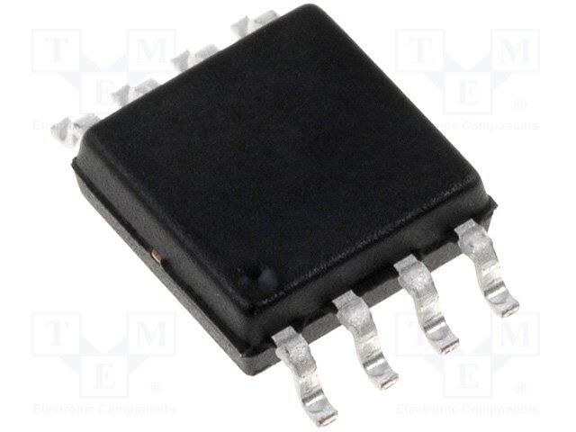
| 供应商器件封装 | 8-SO |
| 其它名称 | 497-13502-1 |
| 内部驱动器 | 是 |
| 准确性 | 7 % |
| 包装 | 剪切带 (CT) |
| 商标 | STMicroelectronics |
| 安装类型 | 表面贴装 |
| 安装风格 | SMD/SMT |
| 封装 | Reel |
| 封装/外壳 | 8-SOIC(0.154",3.90mm 宽) |
| 封装/箱体 | SO-8 |
| 工作温度 | - |
| 工作温度范围 | - 40 C to + 150 C |
| 工厂包装数量 | 2500 |
| 恒压 | - |
| 恒流 | 是 |
| 拓扑 | 高端,低端,PWM,降压(降压) |
| 标准包装 | 1 |
| 特色产品 | http://www.digikey.cn/product-highlights/zh/led200020015000-series/51158 |
| 电压-电源 | 3 V ~ 18 V |
| 电压-输出 | - |
| 电源电压-最大 | 18 V |
| 电源电压-最小 | 3 V |
| 电源电流 | 3 A |
| 类型-初级 | 通用 |
| 类型-次级 | 高亮度 LED(HBLED) |
| 系列 | LED2000 |
| 输入电压范围 | 3 V to 18 V |
| 输出数 | 1 |
| 频率 | 700kHz ~ 1MHz |


- 商务部:美国ITC正式对集成电路等产品启动337调查
- 曝三星4nm工艺存在良率问题 高通将骁龙8 Gen1或转产台积电
- 太阳诱电将投资9.5亿元在常州建新厂生产MLCC 预计2023年完工
- 英特尔发布欧洲新工厂建设计划 深化IDM 2.0 战略
- 台积电先进制程称霸业界 有大客户加持明年业绩稳了
- 达到5530亿美元!SIA预计今年全球半导体销售额将创下新高
- 英特尔拟将自动驾驶子公司Mobileye上市 估值或超500亿美元
- 三星加码芯片和SET,合并消费电子和移动部门,撤换高东真等 CEO
- 三星电子宣布重大人事变动 还合并消费电子和移动部门
- 海关总署:前11个月进口集成电路产品价值2.52万亿元 增长14.8%


PDF Datasheet 数据手册内容提取
LED2000 3 A monolithic step-down current source with synchronous rectification Datasheet - production data Applications High brightness LED driving Halogen bulb replacement General lighting Signage VFQFPN8 4x4 SO8 Description Features The LED2000 is an 850 kHz fixed switching frequency monolithic step-down DC-DC converter 3.0 V to 18 V operating input voltage range designed to operate as precise constant current source with an adjustable current capability up to 850 kHz fixed switching frequency 3 A DC. The embedded PWM dimming circuitry 100 mV typ. current sense voltage drop features LED brightness control. The regulated PWM dimming output current is set connecting a sensing resistor to the feedback pin. The embedded synchronous 7% output current accuracy rectification and the 100 mV typical R Synchronous rectification SENSE voltage drop enhance the efficiency performance. 95 mHS / 69 m LS typical R The size of the overall application is minimized DS(on) Peak current mode architecture thanks to the high switching frequency and ceramic output capacitor compatibility. The device Embedded compensation network is fully protected against thermal overheating, Internal current limiting overcurrent and output short-circuit. The Ceramic output capacitor compliant LED2000 is available in VFQFPN 4 mm x 4 mm 8-lead, and standard SO8 package. Thermal shutdown Figure 1. Typical application circuit (cid:47)(cid:47)(cid:40)(cid:40)(cid:39)(cid:39)(cid:21)(cid:21)(cid:19)(cid:19)(cid:19)(cid:19)(cid:19)(cid:19) (cid:47)(cid:47) (cid:57)(cid:57)(cid:44)(cid:44)(cid:49)(cid:49) (cid:25) (cid:57)(cid:44)(cid:49)(cid:66)(cid:54)(cid:58) (cid:54)(cid:58) (cid:26) (cid:20) (cid:57)(cid:44)(cid:49)(cid:66)(cid:36) (cid:39)(cid:39)(cid:44)(cid:44)(cid:48)(cid:48) (cid:21) (cid:39)(cid:44)(cid:48) (cid:41)(cid:37) (cid:22) (cid:51)(cid:42)(cid:49)(cid:39) (cid:40)(cid:51) (cid:36)(cid:42)(cid:49)(cid:39) (cid:38)(cid:38)(cid:44)(cid:44)(cid:49)(cid:49) (cid:38)(cid:38)(cid:41)(cid:41)(cid:47)(cid:47)(cid:55)(cid:55) (cid:53)(cid:53)(cid:54)(cid:54) (cid:38)(cid:38)(cid:50)(cid:50)(cid:56)(cid:56)(cid:55)(cid:55) (cid:27) (cid:28) (cid:23) (cid:42)(cid:42)(cid:49)(cid:49)(cid:39)(cid:39) (cid:36)(cid:48)(cid:20)(cid:21)(cid:27)(cid:28)(cid:21)(cid:89)(cid:20) June 2013 DocID023432 Rev 4 1/40 This is information on a product in full production. www.st.com
Contents LED2000 Contents 1 Pin settings . . . . . . . . . . . . . . . . . . . . . . . . . . . . . . . . . . . . . . . . . . . . . . . . 6 1.1 Pin connection . . . . . . . . . . . . . . . . . . . . . . . . . . . . . . . . . . . . . . . . . . . . . . 6 1.2 Pin description . . . . . . . . . . . . . . . . . . . . . . . . . . . . . . . . . . . . . . . . . . . . . . 6 2 Maximum ratings . . . . . . . . . . . . . . . . . . . . . . . . . . . . . . . . . . . . . . . . . . . . 7 3 Thermal data . . . . . . . . . . . . . . . . . . . . . . . . . . . . . . . . . . . . . . . . . . . . . . . 7 4 Electrical characteristics . . . . . . . . . . . . . . . . . . . . . . . . . . . . . . . . . . . . . 8 5 Functional description . . . . . . . . . . . . . . . . . . . . . . . . . . . . . . . . . . . . . . . 9 5.1 Power supply and voltage reference . . . . . . . . . . . . . . . . . . . . . . . . . . . . 10 5.2 Voltage monitor . . . . . . . . . . . . . . . . . . . . . . . . . . . . . . . . . . . . . . . . . . . . 10 5.3 Soft-start . . . . . . . . . . . . . . . . . . . . . . . . . . . . . . . . . . . . . . . . . . . . . . . . . . 10 5.4 Error amplifier . . . . . . . . . . . . . . . . . . . . . . . . . . . . . . . . . . . . . . . . . . . . . . 10 5.5 Thermal shutdown . . . . . . . . . . . . . . . . . . . . . . . . . . . . . . . . . . . . . . . . . . .11 6 Application notes . . . . . . . . . . . . . . . . . . . . . . . . . . . . . . . . . . . . . . . . . . 12 6.1 Closing the loop . . . . . . . . . . . . . . . . . . . . . . . . . . . . . . . . . . . . . . . . . . . . 12 6.2 G (s) control to output transfer function . . . . . . . . . . . . . . . . . . . . . . . . 12 CO 6.3 Error amplifier compensation network . . . . . . . . . . . . . . . . . . . . . . . . . . . 13 6.4 LED small signal model . . . . . . . . . . . . . . . . . . . . . . . . . . . . . . . . . . . . . . 15 6.5 Total loop gain . . . . . . . . . . . . . . . . . . . . . . . . . . . . . . . . . . . . . . . . . . . . . 17 6.6 Dimming operation . . . . . . . . . . . . . . . . . . . . . . . . . . . . . . . . . . . . . . . . . . 19 Dimming frequency vs. dimming depth . . . . . . . . . . . . . . . . . . . . . . . . . . . . . . . . . 20 6.7 eDesign studio software . . . . . . . . . . . . . . . . . . . . . . . . . . . . . . . . . . . . . . 21 7 Application information . . . . . . . . . . . . . . . . . . . . . . . . . . . . . . . . . . . . . 22 7.1 Component selection . . . . . . . . . . . . . . . . . . . . . . . . . . . . . . . . . . . . . . . . 22 7.1.1 Sensing resistor . . . . . . . . . . . . . . . . . . . . . . . . . . . . . . . . . . . . . . . . . . . 22 7.1.2 Inductor and output capacitor selection . . . . . . . . . . . . . . . . . . . . . . . . . 22 7.1.3 Input capacitor . . . . . . . . . . . . . . . . . . . . . . . . . . . . . . . . . . . . . . . . . . . . 24 2/40 DocID023432 Rev 4
LED2000 Contents 7.2 Layout considerations . . . . . . . . . . . . . . . . . . . . . . . . . . . . . . . . . . . . . . . 26 7.3 Thermal considerations . . . . . . . . . . . . . . . . . . . . . . . . . . . . . . . . . . . . . . 27 7.4 Short-circuit protection . . . . . . . . . . . . . . . . . . . . . . . . . . . . . . . . . . . . . . . 28 7.5 Application circuit . . . . . . . . . . . . . . . . . . . . . . . . . . . . . . . . . . . . . . . . . . . 30 8 Typical characteristics . . . . . . . . . . . . . . . . . . . . . . . . . . . . . . . . . . . . . . 34 9 Package information . . . . . . . . . . . . . . . . . . . . . . . . . . . . . . . . . . . . . . . . 36 10 Ordering information . . . . . . . . . . . . . . . . . . . . . . . . . . . . . . . . . . . . . . . 39 11 Revision history . . . . . . . . . . . . . . . . . . . . . . . . . . . . . . . . . . . . . . . . . . . 39 DocID023432 Rev 4 3/40 40
List of tables LED2000 List of tables Table 1. Pin description . . . . . . . . . . . . . . . . . . . . . . . . . . . . . . . . . . . . . . . . . . . . . . . . . . . . . . . . . . . 6 Table 2. Absolute maximum ratings. . . . . . . . . . . . . . . . . . . . . . . . . . . . . . . . . . . . . . . . . . . . . . . . . . 7 Table 3. Thermal data. . . . . . . . . . . . . . . . . . . . . . . . . . . . . . . . . . . . . . . . . . . . . . . . . . . . . . . . . . . . . 7 Table 4. Electrical characteristics. . . . . . . . . . . . . . . . . . . . . . . . . . . . . . . . . . . . . . . . . . . . . . . . . . . . 8 Table 5. Uncompensated error amplifier characteristics. . . . . . . . . . . . . . . . . . . . . . . . . . . . . . . . . . 11 Table 6. Inductor selection . . . . . . . . . . . . . . . . . . . . . . . . . . . . . . . . . . . . . . . . . . . . . . . . . . . . . . . . 24 Table 7. List of ceramic capacitors for the LED2000 . . . . . . . . . . . . . . . . . . . . . . . . . . . . . . . . . . . . 25 Table 8. Component list . . . . . . . . . . . . . . . . . . . . . . . . . . . . . . . . . . . . . . . . . . . . . . . . . . . . . . . . . . 31 Table 9. VFQFPN8 (4 x 4 x 1.08 mm) mechanical data. . . . . . . . . . . . . . . . . . . . . . . . . . . . . . . . . . 37 Table 10. SO8 mechanical data. . . . . . . . . . . . . . . . . . . . . . . . . . . . . . . . . . . . . . . . . . . . . . . . . . . . . 38 Table 11. Ordering information. . . . . . . . . . . . . . . . . . . . . . . . . . . . . . . . . . . . . . . . . . . . . . . . . . . . . . 39 Table 12. Document revision history . . . . . . . . . . . . . . . . . . . . . . . . . . . . . . . . . . . . . . . . . . . . . . . . . 39 4/40 DocID023432 Rev 4
LED2000 List of figures List of figures Figure 1. Typical application circuit . . . . . . . . . . . . . . . . . . . . . . . . . . . . . . . . . . . . . . . . . . . . . . . . . . . 1 Figure 2. Pin connection (top view) . . . . . . . . . . . . . . . . . . . . . . . . . . . . . . . . . . . . . . . . . . . . . . . . . . . 6 Figure 3. LED2000 block diagram. . . . . . . . . . . . . . . . . . . . . . . . . . . . . . . . . . . . . . . . . . . . . . . . . . . . 9 Figure 4. Internal circuit. . . . . . . . . . . . . . . . . . . . . . . . . . . . . . . . . . . . . . . . . . . . . . . . . . . . . . . . . . . 10 Figure 5. Block diagram of the loop. . . . . . . . . . . . . . . . . . . . . . . . . . . . . . . . . . . . . . . . . . . . . . . . . . 12 Figure 6. Transconductance embedded error amplifier. . . . . . . . . . . . . . . . . . . . . . . . . . . . . . . . . . . 14 Figure 7. Equivalent series resistor . . . . . . . . . . . . . . . . . . . . . . . . . . . . . . . . . . . . . . . . . . . . . . . . . . 16 Figure 8. Load equivalent circuit . . . . . . . . . . . . . . . . . . . . . . . . . . . . . . . . . . . . . . . . . . . . . . . . . . . . 16 Figure 9. Module plot. . . . . . . . . . . . . . . . . . . . . . . . . . . . . . . . . . . . . . . . . . . . . . . . . . . . . . . . . . . . . 18 Figure 10. Phase plot. . . . . . . . . . . . . . . . . . . . . . . . . . . . . . . . . . . . . . . . . . . . . . . . . . . . . . . . . . . . . . 18 Figure 11. Dimming operation example. . . . . . . . . . . . . . . . . . . . . . . . . . . . . . . . . . . . . . . . . . . . . . . . 19 Figure 12. LED current falling edge operation. . . . . . . . . . . . . . . . . . . . . . . . . . . . . . . . . . . . . . . . . . . 20 Figure 13. Dimming signal. . . . . . . . . . . . . . . . . . . . . . . . . . . . . . . . . . . . . . . . . . . . . . . . . . . . . . . . . . 21 Figure 14. eDesign studio screenshot. . . . . . . . . . . . . . . . . . . . . . . . . . . . . . . . . . . . . . . . . . . . . . . . . 21 Figure 15. Equivalent circuit. . . . . . . . . . . . . . . . . . . . . . . . . . . . . . . . . . . . . . . . . . . . . . . . . . . . . . . . . 23 Figure 16. Layout example . . . . . . . . . . . . . . . . . . . . . . . . . . . . . . . . . . . . . . . . . . . . . . . . . . . . . . . . . 26 Figure 17. Switching losses. . . . . . . . . . . . . . . . . . . . . . . . . . . . . . . . . . . . . . . . . . . . . . . . . . . . . . . . . 27 Figure 18. Constant current protection triggering hiccup mode. . . . . . . . . . . . . . . . . . . . . . . . . . . . . . 30 Figure 19. Demonstration board application circuit . . . . . . . . . . . . . . . . . . . . . . . . . . . . . . . . . . . . . . . 30 Figure 20. PCB layout (component side) VFQFPN package. . . . . . . . . . . . . . . . . . . . . . . . . . . . . . . . 31 Figure 21. PCB layout (bottom side) VFQFPN package . . . . . . . . . . . . . . . . . . . . . . . . . . . . . . . . . . . 32 Figure 22. PCB layout (component side) SO8 package . . . . . . . . . . . . . . . . . . . . . . . . . . . . . . . . . . . 32 Figure 23. PCB layout (bottom side) SO8 package. . . . . . . . . . . . . . . . . . . . . . . . . . . . . . . . . . . . . . . 33 Figure 24. Soft-start. . . . . . . . . . . . . . . . . . . . . . . . . . . . . . . . . . . . . . . . . . . . . . . . . . . . . . . . . . . . . . . 34 Figure 25. Load regulation. . . . . . . . . . . . . . . . . . . . . . . . . . . . . . . . . . . . . . . . . . . . . . . . . . . . . . . . . . 34 Figure 26. Dimming operation . . . . . . . . . . . . . . . . . . . . . . . . . . . . . . . . . . . . . . . . . . . . . . . . . . . . . . . 34 Figure 27. LED current rising edge . . . . . . . . . . . . . . . . . . . . . . . . . . . . . . . . . . . . . . . . . . . . . . . . . . . 34 Figure 28. LED current falling edge. . . . . . . . . . . . . . . . . . . . . . . . . . . . . . . . . . . . . . . . . . . . . . . . . . . 35 Figure 29. Hiccup current protection . . . . . . . . . . . . . . . . . . . . . . . . . . . . . . . . . . . . . . . . . . . . . . . . . . 35 Figure 30. Efficiency vs. IOUT (VIN 32 V). . . . . . . . . . . . . . . . . . . . . . . . . . . . . . . . . . . . . . . . . . . . . . 35 Figure 31. Thermal shutdown protection. . . . . . . . . . . . . . . . . . . . . . . . . . . . . . . . . . . . . . . . . . . . . . . 35 Figure 32. VFQFPN8 (4 x 4 x 1.08 mm) package outline . . . . . . . . . . . . . . . . . . . . . . . . . . . . . . . . . . 36 Figure 33. SO8 package outline . . . . . . . . . . . . . . . . . . . . . . . . . . . . . . . . . . . . . . . . . . . . . . . . . . . . . 38 DocID023432 Rev 4 5/40 40
Pin settings LED2000 1 Pin settings 1.1 Pin connection Figure 2. Pin connection (top view) SW 1 8 VINSW DIM PGND GND VINA AGND NC DIM 4 5 FB SO8-BW VFQFPN AM12893v1 1.2 Pin description Table 1. Pin description Package/pin Type Description VFQFPN S08-BW 1 3 VIN Analog circuitry power supply connection A Dimming control input. Logic low prevents the switching activity, logic high enables it. A square wave on this pin 2 4 DIM implements LED current PWM dimming. Connect to VIN if A not used (see Section6.6) Feedback input. Connect a proper sensing resistor to set the 3 5 FB LED current 4 6 AGND Analog circuitry ground connection 5 - NC Not connected 6 8 V Power input voltage INSW 7 1 SW Regulator switching pin 8 2 PGND Power ground - 7 GND Connect to AGND 6/40 DocID023432 Rev 4
LED2000 Maximum ratings 2 Maximum ratings Table 2. Absolute maximum ratings Symbol Parameter Value Unit V Power input voltage -0.3 to 20 INSW V Input voltage -0.3 to 20 INA V Dimming voltage -0.3 to V DIM INA V V Output switching voltage -1 to V SW IN V Power Good -0.3 to V PG IN V Feedback voltage -0.3 to 2.5 FB I FB current -1 to +1 mA FB P Power dissipation at T < 60 °C 2 W TOT A T Operating junction temperature range -40 to 150 °C OP T Storage temperature range -55 to 150 °C stg 3 Thermal data Table 3. Thermal data Symbol Parameter Value Unit Maximum thermal resistance VFQFPN 40 R °C/W thJA junction-ambient(1) SO8-BW 65 1. Package mounted on demonstration board. DocID023432 Rev 4 7/40 40
Electrical characteristics LED2000 4 Electrical characteristics T = 25 °C, V = 12 V, unless otherwise specified. J CC Table 4. Electrical characteristics Value Symbol Parameter Test conditions Unit Min. Typ. Max. Operating input voltage range See(1) 3 18 V Device ON level 2.6 2.75 2.9 V IN Device OFF level 2.4 2.55 2.7 T = 25 °C 90 97 104 J V Feedback voltage mV FB T = 125 °C 90 100 110 J I V pin bias current See(1) 600 nA FB FB R -P High-side switch on-resistance I = 750 mA 95 m DSON SW R -N Low-side switch on-resistance I = 750 mA 69 m DSON SW I Maximum limiting current See(2) 5 A LIM Oscillator F Switching frequency 0.7 0.85 1 MHz SW D Duty cycle See(2) 0 100 % DC characteristics I Quiescent current 1.5 2.5 mA Q Dimming Switching activity 1.2 VDIM DIM threshold voltage Switching activity V 0.4 prevented I DIM current 2 A DIM Soft-start T Soft-start duration 1 ms SS Protection Thermal shutdown 150 T °C SHDN Hystereris 15 1. Specifications referred to T from -40 to +125 °C. Specifications in the -40 to +125 °C temperature range J are assured by design, characterization and statistical correlation. 2. Guaranteed by design. 8/40 DocID023432 Rev 4
LED2000 Functional description 5 Functional description The LED2000 device is based on a “peak current mode” architecture with fixed frequency control. As a consequence, the intersection between the error amplifier output and the sensed inductor current generates the control signal to drive the power switch. The main internal blocks shown in the block diagram in Figure3 are: High-side and low-side embedded power element for synchronous rectification A fully integrated sawtooth oscillator with a typical frequency of 850 kHz A transconductance error amplifier A high-side current sense amplifier to track the inductor current A pulse width modulator (PWM) comparator and the circuitry necessary to drive the internal power element The soft-start circuitry to decrease the inrush current at power-up The current limitation circuit based on the pulse-by-pulse current protection with frequency divider The dimming circuitry for output current PWM The thermal protection function circuitry. Figure 3. LED2000 block diagram VINA VIN SW OCP OSC REF I2V I_ SENSE RSENSE COMP REGULATOR UVLO OCP Vdrv_p DRIVER MOSFET Vsum CONTROL LOGIC PWM Vdrv_n Vc SW OTP DMD E/A DIMMING DRIVER SOFT-START 0.1V FB DIM GNDA GNDP AM12894v1 DocID023432 Rev 4 9/40 40
Functional description LED2000 5.1 Power supply and voltage reference The internal regulator circuit consists of a startup circuit, an internal voltage pre-regulator, the BandGap voltage reference and the bias block that provides current to all the blocks. The starter supplies the startup current to the entire device when the input voltage goes high and the device is enabled. The pre-regulator block supplies the BandGap cell with a pre- regulated voltage that has a very low supply voltage noise sensitivity. 5.2 Voltage monitor An internal block continuously senses the V , V and V . If the monitored voltages are CC ref bg good, the regulator begins operating. There is also a hysteresis on the V (UVLO). CC Figure 4. Internal circuit Vcc STARTER PREREGULATOR VREG BANDGAP IC BIAS AM12895v1 D00IN126 VREF 5.3 Soft-start The startup phase is implemented ramping the reference of the embedded error amplifier in 1 ms typ. time. It minimizes the inrush current and decreases the stress of the power components at power-up. During normal operation a new soft-start cycle takes place in case of: Thermal shutdown event UVLO event. The soft-start is disabled when DIM input goes high in order to maximize the dimming performance. 5.4 Error amplifier The voltage error amplifier is the core of the loop regulation. It is a transconductance operational amplifier whose non-inverting input is connected to the internal voltage reference (100 mV), while the inverting input (FB) is connected to the output current sensing resistor. The error amplifier is internally compensated to minimize the size of the final application. 10/40 DocID023432 Rev 4
LED2000 Functional description Table 5. Uncompensated error amplifier characteristics Description Value Transconductance 250 µS Low frequency gain 96 dB C 195 pF C R 70 K C The error amplifier output is compared with the inductor current sense information to perform PWM control. 5.5 Thermal shutdown The shutdown block generates a signal that disables the power stage if the temperature of the chip goes higher than a fixed internal threshold (150 ± 10 °C typical). The sensing element of the chip is close to the PDMOS area, ensuring fast and accurate temperature detection. A 15 °C typical hysteresis prevents the device from turning ON and OFF continuously during the protection operation. DocID023432 Rev 4 11/40 40
Application notes LED2000 6 Application notes 6.1 Closing the loop Figure 5. Block diagram of the loop PWM control VIN GCO(s) Current sense HS switch L VOUT LC filter LS switch COUT - error - FB amplifier PWM + VCONTROL comparator + VREF RC compensation RS network CC α LED A (s) O 6.2 G (s) control to output transfer function CO The accurate control to output transfer function for a buck peak current mode converter can be written as: Equation 1 s 1+------ R0 1 z G s = ---------------------------------------------------------------------------------------------------------------------F s CO Ri 1+R-----0------L-T----S----W---mC1–D–0,5 1+--s---p- H where R represents the load resistance, R the equivalent sensing resistor of the current 0 i sense circuitry, the single pole introduced by the LC filter and the zero given by the p z ESR of the output capacitor. F (s) accounts for the sampling effect performed by the PWM comparator on the output of H the error amplifier that introduces a double pole at one half of the switching frequency. 12/40 DocID023432 Rev 4
LED2000 Application notes Equation 2 1 = ------------------------------- Z ESRC OUT Equation 3 1 mC1–D–0,5 = --------------------------------------+--------------------------------------------- P R C LC f LOAD OUT OUT SW where: Equation 4 Se mC = 1+S------ n S = V f e pp SW V –V IN OUT S = ------------------------------R n L i S represents the slope of the sensed inductor current, S the slope of the external ramp n e (V peak-to-peak amplitude) that implements the slope compensation to avoid sub- PP harmonic oscillations at duty cycle over 50%. The sampling effect contribution F (s) is: H Equation 5 1 F s = ------------------------------------------- H 2 s s 1+-------------------+------ Q 2 n P n where: Equation 6 = f n SW and Equation 7 1 Q = ---------------------------------------------------------- P m 1–D–0,5 C 6.3 Error amplifier compensation network The LED2000 device embeds (see Figure6) the error amplifier and a pre-defined compensation network which is effective in stabilizing the system in most application conditions. DocID023432 Rev 4 13/40 40
Application notes LED2000 Figure 6. Transconductance embedded error amplifier E/A + COMP FB - R C C P C C V+ R R C C dV 0 0 C P G dV C m C AM12897v1 R and C introduce a pole and a zero in the open loop gain. C does not significantly affect C C P system stability but it is useful to reduce the noise at the output of the error amplifier. The transfer function of the error amplifier and its compensation network is: Equation 8 A 1+sR C V0 c c A s = ----------------------------------------------------------------------------------------------------------------------------------------------------------------------------------------- 0 2 s R C +C R C +sR C +R C +C +R C +1 0 0 p c c 0 c 0 0 p c c where A = G · R . vo m o The poles of this transfer function are (if C >> C + C ): C 0 P Equation 9 1 f = ---------------------------------- P LF 2R C 0 c Equation 10 1 f = ---------------------------------------------------- P HF 2R C +C c 0 p whereas the zero is defined as: Equation 11 1 F = --------------------------------- Z 2R C c c 14/40 DocID023432 Rev 4
LED2000 Application notes The embedded compensation network is R = 70 K, C = 195 pF while C and C can be C C P O considered as negligible. The error amplifier output resistance is 240 Mso the relevant singularities are: Equation 12 f = 116 kHz f = 34 Hz Z P LF 6.4 LED small signal model Once the system reaches the working condition, the LEDs composing the row are biased and their equivalent circuit can be considered as a resistor for frequencies << 1 MHz. The LED manufacturer typically provides the equivalent dynamic resistance of the LED biased at different DC currents. This parameter is required to study the behavior of the system in the small signal analysis. For instance, the equivalent dynamic resistance of the Luxeon III Star from Lumiled measured with different biasing current level is reported below: Equation 13 1,3 ILED= 350mA rLED 0,9 ILED= 700mA If the LED datasheet does not report the equivalent resistor value, it can be simply derived as the tangent to the diode I-V characteristic in the present working point (see Figure7). DocID023432 Rev 4 15/40 40
Application notes LED2000 Figure 7. Equivalent series resistor [A] 1 working point 0.1 1 2 3 4 [V] AM12898v1 Figure8 shows the equivalent circuit of the LED constant current generator. Figure 8. Load equivalent circuit LL Dled1 VIN D Dled2 COUT Rs L Rd1 VIN D1 Rd2 COUT Rs AM12899v1 16/40 DocID023432 Rev 4
LED2000 Application notes As a consequence, the LED equivalent circuit gives the (s) term correlating the output LED voltage with the high impedance FB input: Equation 14 R SENSE n = ---------------------------------------------------------- LED LED n r +R LED LED SENSE 6.5 Total loop gain In summary, the open loop gain can be expressed as: Equation 15 Gs = G sA s n CO 0 LED LED Example 1 Design specification: V = 12 V, V = 3.5 V, n = 2, r = 1.1 , I = 700 mA, I = 2% IN FW_LED LED LED LED LED RIPPLE The inductor and capacitor value are dimensioned in order to meet the I LED RIPPLE specification (see Section7.1.2 for output capacitor and inductor selection guidelines): L = 10 H, C = 2.2 F MLCC (negligible ESR) OUT Accordingly, with Section7.1.1 the sensing resistor value is: Equation 16 100 mV R = ---------------------140 m S 700 mA Equation 17 RSENSE 140 m n = ---------------------------------------------------------- = ------------------------------------------------- = 0,06 LED LED n r +R 21,1+140 m LED LED SENSE The gain and phase margin Bode diagrams are plotted respectively in Figure9 and Figure10. DocID023432 Rev 4 17/40 40
Application notes LED2000 Figure 9. Module plot (cid:40)(cid:59)(cid:55)(cid:40)(cid:53)(cid:49)(cid:36)(cid:47)(cid:3)(cid:47)(cid:50)(cid:50)(cid:51)(cid:3)(cid:48)(cid:50)(cid:39)(cid:56)(cid:47)(cid:40) (cid:20)(cid:19)(cid:19) (cid:27)(cid:26) (cid:26)(cid:23) (cid:25)(cid:20) (cid:37)(cid:64) (cid:72)(cid:3)(cid:62)(cid:71) (cid:23)(cid:27) (cid:88)(cid:79) (cid:82)(cid:71) (cid:22)(cid:24) (cid:48) (cid:21)(cid:21) (cid:28) (cid:23) (cid:20)(cid:26) (cid:22)(cid:19) (cid:19)(cid:17)(cid:20) (cid:20) (cid:20)(cid:19) (cid:20)(cid:19)(cid:19) (cid:20)(cid:17)(cid:20)(cid:19)(cid:22) (cid:20)(cid:17)(cid:20)(cid:19)(cid:23) (cid:20)(cid:17)(cid:20)(cid:19)(cid:24) (cid:20)(cid:17)(cid:20)(cid:19)(cid:25) (cid:20)(cid:17)(cid:20)(cid:19)(cid:26) (cid:41)(cid:85)(cid:72)(cid:84)(cid:88)(cid:72)(cid:81)(cid:70)(cid:92)(cid:3)(cid:62)(cid:43)(cid:93)(cid:64) (cid:36)(cid:48)(cid:20)(cid:21)(cid:28)(cid:19)(cid:19)(cid:89)(cid:20) Figure 10. Phase plot (cid:40)(cid:59)(cid:55)(cid:40)(cid:53)(cid:49)(cid:36)(cid:47)(cid:3)(cid:47)(cid:50)(cid:50)(cid:51)(cid:3)(cid:42)(cid:36)(cid:44)(cid:49)(cid:3)(cid:51)(cid:43)(cid:36)(cid:54)(cid:40) (cid:20)(cid:27)(cid:19) (cid:20)(cid:24)(cid:26)(cid:17)(cid:24) (cid:20)(cid:22)(cid:24) (cid:20)(cid:20)(cid:21)(cid:17)(cid:24) (cid:72)(cid:3) (cid:86) (cid:68) (cid:51)(cid:75) (cid:28)(cid:19) (cid:25)(cid:26)(cid:17)(cid:24) (cid:23)(cid:24) (cid:21)(cid:21)(cid:17)(cid:24) (cid:19)(cid:19)(cid:17)(cid:20) (cid:20) (cid:20)(cid:19) (cid:20)(cid:19)(cid:19) (cid:20)(cid:17)(cid:20)(cid:19)(cid:22) (cid:20)(cid:17)(cid:20)(cid:19)(cid:23) (cid:20)(cid:17)(cid:20)(cid:19)(cid:24) (cid:20)(cid:17) (cid:25) (cid:20)(cid:17)(cid:20)(cid:19)(cid:26) (cid:41)(cid:85)(cid:72)(cid:84)(cid:88)(cid:72)(cid:81)(cid:70)(cid:92)(cid:3)(cid:62)(cid:43)(cid:93)(cid:64) (cid:36)(cid:48)(cid:20)(cid:21)(cid:28)(cid:19)(cid:20)(cid:89)(cid:20) The cut-off frequency and the phase margin are: Equation 18 f = 100 kHz pm = 47 C 18/40 DocID023432 Rev 4
LED2000 Application notes 6.6 Dimming operation The dimming input disables the switching activity, masking the PWM comparator output. The inductor current dynamic when dimming input goes high depends on the designed system response. The best dimming performance is obtained maximizing the bandwidth and phase margin, when it is possible. As a general rule, the output capacitor minimization improves the dimming performance. Figure 11. Dimming operation example AM12902v1 In fact, when dimming enables the switching activity, a small capacitor value is fast charged with low inductor value. As a consequence, the LEDs current rising edge time is improved and the inductor current oscillation reduced. An oversized output capacitor value requires extra current for fast charge so generating certain inductor current oscillations The switching activity is prevented as soon as the dimming signal goes low. Nevertheless, the LED current drops to zero only when the voltage stored in the output capacitor goes below a minimum voltage determined by the selected LEDs. As a consequence, a big capacitor value makes the LED current falling time worse than a smaller one. The LED2000 embeds dedicated circuitry to improve LED current falling time. As soon as the dimming input goes low, the low-side is kept enabled to discharge C until OUT the LED current drops to 60% of the nominal current. A negative current limitation (-1 A typical) protects the device during this operation (see Figure12). DocID023432 Rev 4 19/40 40
Application notes LED2000 Figure 12. LED current falling edge operation AM12903v1 Dimming frequency vs. dimming depth As seen in Section6.6, the LEDs current rising and falling edge time mainly depends on the system bandwidth (T ) and the selected output capacitor value (T and T ). RISE RISE FALL The dimming performance depends on the minimum current pulse shape specification of the final application. The ideal minimum current pulse has rectangular shape, however, it degenerates into a trapezoid or, at worst, into a triangle, depending on the ratio (T + T ) / T . RISE FALL DIM Equation 19 rectangle trapezoid triangle T +T T +T T +T RISE FALL RISE FALL RISE FALL ---------------------------------------------«1 ---------------------------------------------1 --------------------------------------------- = 1 T T T DIM DIM DIM The small signal response in Figure11 and Figure12 is considered as an example. Equation 20 TRISE20s TFALL5s Assuming the minimum current pulse shape specification as: Equation 21: T +T = 0,5T = 0,5D T RISE FALL MIN_PULSE MIN DIMMING it is possible to calculate the maximum dimming depth given the dimming frequency or vice versa. 20/40 DocID023432 Rev 4
LED2000 Application notes Figure 13. Dimming signal AM12904v1 For example, assuming a 1 kHz dimming frequency the maximum dimming depth is 5% or, given a 2% dimming depth, it follows a 200 Hz maximum f . DIM The LED2000 dimming performance is strictly dependent on the system small signal response. As a consequence, an optimized compensation (good phase margin and bandwidth maximized) and minimized C value are crucial for the best performance. OUT 6.7 eDesign studio software The LED2000 device is supported by the eDesign software which can be viewed online at www.st.com. Figure 14. eDesign studio screenshot AM12905v1 The software easily supports the component sizing according to the technical information given in this datasheet (see Section6 and Section7). The end user is requested to fill in the requested information such as the input voltage range, the selected LED parameters and the number of LEDs composing the row. DocID023432 Rev 4 21/40 40
Application information LED2000 The software calculates external components according to the internal database. It is also possible to define new components and ask the software to use them. Bode plots, estimated efficiency and thermal performance are provided. Finally, the user can save the design and print all the information including the bill of material of the board. 7 Application information 7.1 Component selection 7.1.1 Sensing resistor In closed loop operation the LED2000 feedback pin voltage is 100 mV, so the sensing resistor calculation is expressed as: Equation 22 100 mV R = -------------------- S I LED Since the main loop (see Section6.1) regulates the sensing resistor voltage drop, the average current is regulated into the LEDs. The integration period is at minimum 5 * T SW since the system bandwidth can be dimensioned up to F /5 at maximum. SW The system performs the output current regulation over a period which is at least five times longer than the switching frequency. The output current regulation neglects the ripple current contribution and its reliance on external parameters like input voltage and output voltage variations (line transient and LED forward voltage spread). This performance can not be achieved with simpler regulation loops such as a hysteretic control. For the same reason, the switching frequency is constant over the application conditions, which helps to tune the EMI filtering and to guarantee the maximum LED current ripple specification in the application range. This performance can not be achieved using constant ON/OFF-time architecture. 7.1.2 Inductor and output capacitor selection The output capacitor filters the inductor current ripple that, given the application condition, depends on the inductor value. As a consequence, the LED current ripple, that is the main specification for a switching current source, depends on the inductor and output capacitor selection. 22/40 DocID023432 Rev 4
LED2000 Application information Figure 15. Equivalent circuit (cid:39)(cid:38)(cid:53) (cid:47)(cid:47) (cid:39)(cid:38)(cid:53) (cid:47) (cid:39)(cid:79)(cid:72)(cid:71)(cid:20) (cid:53)(cid:71)(cid:20) (cid:40)(cid:54)(cid:53) (cid:40)(cid:54)(cid:53) (cid:21) (cid:21) (cid:57)(cid:44)(cid:49) (cid:39)(cid:39) (cid:39)(cid:79)(cid:72)(cid:71)(cid:81) (cid:57)(cid:44)(cid:49) (cid:39)(cid:39) (cid:53)(cid:71)(cid:81) (cid:20) (cid:20) (cid:38)(cid:50)(cid:56)(cid:55) (cid:38)(cid:50)(cid:56)(cid:55) (cid:53)(cid:86) (cid:53)(cid:86) (cid:36)(cid:48)(cid:20)(cid:21)(cid:28)(cid:19)(cid:25)(cid:89)(cid:20) The LED ripple current can be calculated as the inductor ripple current ratio flowing into the output impedance using the Laplace transform (see Figure11): Equation 23 8 ------I 1+sESRC 2 L OUT I s = ----------------------------------------------------------------------------------------------------------- RIPPLE 1+sR +ESR+n R C S LED LED OUT where the term 8/2 represents the main harmonic of the inductor current ripple (which has a triangular shape) and I is the inductor current ripple. L Equation 24 V n V +100mV OUT LED FW_LED I = --------------T = ------------------------------------------------------------------T L L OFF L OFF so L value can be calculated as: Equation 25 n V +100mV n V +100mV n V +100mV LED FW_LED LED FW_LED LED FW_LED L = ------------------------------------------------------------------T = ------------------------------------------------------------------ 1–------------------------------------------------------------------ I OFF I V L L IN where T is the OFF-time of the embedded high switch, given by 1-D. OFF As a consequence, the lower the inductor value (so the higher the current ripple), the higher the C value would be to meet the specification. OUT A general rule to dimension L value is: Equation 26 I L ----------- 0,5 I LED Finally, the required output capacitor value can be calculated equalizing the LED current ripple specification with the module of the Fourier transformer (see Equation23) calculated at F frequency. SW DocID023432 Rev 4 23/40 40
Application information LED2000 Equation 27 I s=j = I RIPPLE RIPPLE_SPEC Example 2(see Example 1): V = 12 V, I = 700 mA, /I = 2%, V = 3.5 V, n = 2. IN LED ILED LED FW_LED LED A lower inductor value maximizes the inductor current slew rate for better dimming performance. Equation26 becomes: Equation 28 I L ----------- = 0,5 I LED which is satisfied selecting a10 H inductor value. The output capacitor value must be dimensioned according to Equation27. Finally, given the selected inductor value, a 2.2 F ceramic capacitor value keeps the LED current ripple ratio lower than the 2% of the nominal current. An output ceramic capacitor type (negligible ESR) is suggested to minimize the ripple contribution given a fixed capacitor value. Table 6. Inductor selection Manufacturer Series Inductor value (µH) Saturation current (A) WE-HCI 7040 1 to 4.7 20 to 7 Würth Elektronik WE-HCI 7050 4.9 to 10 20 to 4.0 Coilcraft XPL 7030 2.2 to 10 29 to 7.2 7.1.3 Input capacitor The input capacitor must be able to support the maximum input operating voltage and the maximum RMS input current. Since step-down converters draw current from the input in pulses, the input current is squared and the height of each pulse is equal to the output current. The input capacitor must absorb all this switching current, whose RMS value can be up to the load current divided by two (worst case, with duty cycle of 50%). For this reason, the quality of these capacitors must be very high to minimize the power dissipation generated by the internal ESR, thereby improving system reliability and efficiency. The critical parameter is usually the RMS current rating, which must be higher than the RMS current flowing through the capacitor. The maximum RMS input current (flowing through the input capacitor) is: Equation 29 2 2 2D D I = I D–---------------+------- RMS O 2 24/40 DocID023432 Rev 4
LED2000 Application information where is the expected system efficiency, D is the duty cycle and I is the output DC O current. Considering = 1 this function reaches its maximum value at D = 0.5 and the equivalent RMS current is equal to I divided by 2. The maximum and minimum duty cycles O are: Equation 30 V +V OUT F D = ------------------------------------- MAX V –V INMIN SW and Equation 31 V +V OUT F D = -------------------------------------- MIN V –V INMAX SW where V is the free-wheeling diode forward voltage and V the voltage drop across the F SW internal PDMOS. Considering the range D to D , it is possible to determine the max. MIN MAX I going through the input capacitor. Capacitors that can be considered are: RMS Electrolytic capacitors: These are widely used due to their low price and their availability in a wide range of RMS current ratings. The only drawback is that, considering ripple current rating requirements, they are physically larger than other capacitors. Ceramic capacitors: If available for the required value and voltage rating, these capacitors usually have a higher RMS current rating for a given physical dimension (due to very low ESR). The drawback is the considerably high cost. Tantalum capacitors: Small tantalum capacitors with very low ESR are becoming more widely available. However, they can occasionally burn if subjected to very high current during charge. Therefore, it is suggested to avoid this type of capacitor for the input filter of the device as they may be stressed by a high surge current when connected to the power supply. Table 7. List of ceramic capacitors for the LED2000 Manufacturer Series Capacitor value (µC) Rated voltage (V) TAIYO YUDEN UMK325BJ106MM-T 10 50 MURATA GRM42-2 X7R 475K 50 4.7 50 If the selected capacitor is ceramic (so neglecting the ESR contribution), the input voltage ripple can be calculated as: Equation 32 IO D D V = ----------------------- 1–---- D+----1–D IN PP C f IN SW DocID023432 Rev 4 25/40 40
Application information LED2000 7.2 Layout considerations The layout of switching DC-DC converters is very important to minimize noise and interference. Power-generating portions of the layout are the main cause of noise and so high switching current loop areas should be kept as small as possible and lead lengths as short as possible. High impedance paths (in particular the feedback connections) are susceptible to interference, so they should be as far as possible from the high current paths. A layout example is provided in Figure16. The input and output loops are minimized to avoid radiation and high frequency resonance problems. The feedback pin to the sensing resistor path must be designed as short as possible to avoid pick-up noise. Another important issue is the ground plane of the board. As the package has an exposed pad, it is very important to connect it to an extended ground plane in order to reduce the thermal resistance junction-to-ambient. To increase the design noise immunity, different signal and power ground should be implemented in the layout (see Section7.5: Application circuit). The signal ground serves the small signal components, the device analog ground pin, the exposed pad and a small filtering capacitor connected to the V pin. The power ground serves the device ground pin INA and the input filter. The different grounds are connected underneath the output capacitor. Neglecting the current ripple contribution, the current flowing through this component is constant during the switching activity and so this is the cleanest ground point of the buck application circuit. Figure 16. Layout example 26/40 DocID023432 Rev 4
LED2000 Application information 7.3 Thermal considerations The dissipated power of the device is tied to three different sources: Conduction losses due to the R , which are equal to: DSON Equation 33 2 P = R I D ON RDSON_HS OUT 2 P = R I 1–D OFF RDSON_LS OUT where D is the duty cycle of the application. Note that the duty cycle is theoretically given by the ratio between V (n V + 100 mV) and V , but in practice it is substantially OUT LED LED IN higher than this value to compensate for the losses in the overall application. For this reason, the conduction losses related to the R increase compared to an ideal case. DSON Switching losses due to turn-ON and turn-OFF. These are derived using the following equation: Equation 34 T +T RISE FALL P = V I -----------------------------------------F = V I T F SW IN OUT 2 SW IN OUT SW_EQ SW where T and T represent the switching times of the power element that cause the RISE FALL switching losses when driving an inductive load (see Figure17). T is the equivalent SW switching time. Figure 17. Switching losses AM12908v1 Quiescent current losses. Equation 35 P = V I Q IN Q DocID023432 Rev 4 27/40 40
Application information LED2000 Example 3(see Example 1): V = 12 V, V = 3.5 V, n = 2, I = 700 mA IN FW_LED LED LED The typical output voltage is: Equation 36 V = n V +V = 7,1V OUT LED FW_LED FB R has a typical value of 95 m and R is 69 m at 25 °C. DSON_HS DSON_LS For the calculation we can estimate R = 140 m and R = 100 mas DSON_HS DSON_LS a consequence of T increase during the operation. J T is approximately 12 ns. SW_EQ I has a typical value of 1.5 mA at V = 12 V. Q IN The overall losses are: Equation 37 2 2 P = R I D+R I 1–D+V I f T +V I TOT DSON_HS OUT DSON_LS OUT IN OUT SW SW IN Q Equation 38 2 2 –9 3 –3 P = 0,140,7 0,6+0,10,7 0,4+120,71210 85010 +121,510 205mW TOT The junction temperature of the device is: Equation 39 T = T +Rth P J A J–A TOT where T is the ambient temperature and Rth is the thermal resistance junction-to- A J-A ambient. Thejunction-to-ambient (Rth ) thermal resistance of the device assembled in the J-A HSO8 package and mounted on the board is about 40 °C/W. Assuming the ambient temperature is around 40 °C, the estimated junction temperature is: T = 60+0,2054068C J 7.4 Short-circuit protection In overcurrent protection mode, when the peak current reaches the current limit threshold, the device disables the power element and it is able to reduce the conduction time down to the minimum value (approximately 100 nsec typical) to keep the inductor current limited. This is the pulse-by-pulse current limitation to implement the constant current protection feature. 28/40 DocID023432 Rev 4
LED2000 Application information In overcurrent condition, the duty cycle is strongly reduced and, in most applications, this is enough to limit the switch current to the current threshold. The inductor current ripple during ON and OFF phases can be written as: ON phase Equation 40 V –V –DCR +R I IN OUT L DSON HS I = -----------------------------------------------------------------------------------------------T L TON L ON OFF phase Equation 41 –V +DCR +R I OUT L DSON LS I = ----------------------------------------------------------------------------------------T L TON L OFF where DCR is the series resistance of the inductor. L The pulse-by-pulse current limitation is effective to implement constant current protection when: Equation 42 I = I L TON L TOFF From Equation40 and Equation41 it can be seen that the implementation of the constant current protection becomes more critical the lower the V and the higher the V . OUT IN In fact, in short-circuit condition the voltage applied to the inductor during the OFF-time becomes equal to the voltage drop across parasitic components (typically the DCR of the inductor and the R of the low-side switch) since VOUT is negligible, while during T DSON ON the voltage applied at the inductor is maximized and is approximately equal to V . IN In general, the worst case scenario is heavy short-circuit at the output with maximum input voltage. Equation40 and Equation41 in overcurrent conditions can be simplified to: Equation 43 V –DCR +R I V IN L DSON HS IN I = ------------------------------------------------------------------------T ---------90ns L TON L ON MIN L considering T which has already been reduced to its minimum. ON Equation 44 –DCR +R I –DCR +R I L DSON LS L DSON LS I = --------------------------------------------------------------T –90ns--------------------------------------------------------------1,18s L TOFF L SW L where T = 1/F and considering the nominal F . SW SW SW At higher input voltage I may be higher than I and so the inductor current can L TON L TOFF escalate. As a consequence, the system typically meets Equation42 at a current level DocID023432 Rev 4 29/40 40
Application information LED2000 higher than the nominal value thanks to the increased voltage drop across stray components. In most of the application conditions the pulse-by-pulse current limitation is effective to limit the inductor current. Whenever the current escalates, a second level current protection called “Hiccup mode” is enabled. Hiccup protection offers an additional protection against heavy short-circuit conditions at very high input voltage even considering the spread of the minimum conduction time of the power element. If the hiccup current level (6.2 A typical) is triggered, the switching activity is prevented for 12 cycles. Figure18 shows the operation of the constant current protection when a short-circuit is applied at the output at the maximum input voltage. Figure 18. Constant current protection triggering hiccup mode AM12909v1 7.5 Application circuit Figure 19. Demonstration board application circuit (cid:54)L(cid:55)E(cid:20)D(cid:38)2(cid:38)0(cid:23)0(cid:19)0 (cid:47)(cid:47) (cid:57)(cid:44)(cid:49) (cid:25) (cid:57)(cid:44)(cid:49)(cid:66)(cid:54)(cid:58) (cid:54)(cid:58) (cid:26) (cid:57)(cid:47)(cid:40)(cid:39)(cid:14) (cid:21)(cid:17)(cid:21)(cid:88)(cid:43) (cid:20) (cid:57)(cid:44)(cid:49)(cid:66)(cid:36) (cid:39)(cid:44)(cid:48) (cid:21) (cid:39)(cid:44)(cid:48) (cid:41)(cid:37) (cid:22) (cid:57)(cid:47)(cid:40)(cid:39)(cid:16) (cid:21) (cid:51)(cid:42)(cid:49)(cid:39) (cid:40)(cid:51) (cid:36)(cid:42)(cid:49)(cid:39) (cid:22) (cid:20) (cid:53)(cid:54) (cid:38)(cid:22) (cid:53)(cid:20) (cid:23)(cid:46)(cid:26) (cid:27) (cid:28) (cid:23) (cid:19)(cid:17)(cid:20)(cid:24) (cid:21)(cid:17)(cid:21)(cid:88)(cid:15)(cid:3)(cid:21)(cid:24)(cid:57) (cid:53)(cid:21)(cid:45)(cid:51)(cid:20) (cid:38)(cid:21) (cid:38)(cid:20) (cid:49)(cid:48) (cid:20)(cid:19)(cid:88)(cid:15)(cid:3)(cid:21)(cid:24)(cid:57) (cid:20)(cid:19)(cid:19)(cid:81)(cid:41)(cid:15)(cid:3)(cid:24)(cid:19)(cid:57) (cid:86)(cid:76)(cid:74)(cid:81)(cid:68)(cid:79)(cid:3)(cid:42)(cid:49)(cid:39) (cid:83)(cid:82)(cid:90)(cid:72)(cid:85)(cid:3)(cid:42)(cid:49)(cid:39) (cid:42)(cid:49)(cid:39) (cid:36)(cid:48)(cid:20)(cid:21)(cid:28)(cid:20)(cid:19)(cid:89)(cid:20) 30/40 DocID023432 Rev 4
LED2000 Application information Table 8. Component list Reference Part number Description Manufacturer 100 nF 50 V C1 (size 0805) 10 F 25 V C2 GRM31CR61E106KA12L Murata (size 1206) 2.2 F 25 V C3 GRM21BR71E225KA73L Murata (size 0805) 4.7 K5% R1 (size 0603) R2 Not mounted 0.15 1% Rs ERJ14BSFR15U Panasonic (size 1206) 22 H L1 XAL6060-223ME I = 5.6 A (30% drop) I = 6.9 A (40 C rise) Coilcraft SAT RMS (size 6.36 x 6.56 x 6.1 mm) Figure 20. PCB layout (component side) VFQFPN package DocID023432 Rev 4 31/40 40
Application information LED2000 Figure 21. PCB layout (bottom side) VFQFPN package Figure 22. PCB layout (component side) SO8 package It is strongly recommended that the input capacitors are to be put as close as possible to the pins, see C1 and C2. 32/40 DocID023432 Rev 4
LED2000 Application information Figure 23. PCB layout (bottom side) SO8 package DocID023432 Rev 4 33/40 40
Typical characteristics LED2000 8 Typical characteristics Figure 24. Soft-start Figure 25. Load regulation Vin 12V Vled 7V AM12913v1 AM12914v1 Figure 26. Dimming operation Figure 27. LED current rising edge AM12915v1 AM12916v1 34/40 DocID023432 Rev 4
LED2000 Typical characteristics Figure 28. LED current falling edge Figure 29. Hiccup current protection To maximize the dimming performance the embedded LS discharges COUT when DIM goes low. (DIM = 0 && VFB> 60mV): the low side is enabled as long as IL> -1A (implements negative current limitation) AM12918v1 AM12917v1 Figure 30. Efficiency vs. IOUT (VIN 32 V) Figure 31. Thermal shutdown protection 130 ns typ. AM12920v1 AM12919v1 DocID023432 Rev 4 35/40 40
Package information LED2000 9 Package information In order to meet environmental requirements, ST offers these devices in different grades of ECOPACK® packages, depending on their level of environmental compliance. ECOPACK specifications, grade definitions and product status are available at: www.st.com. ECOPACK is an ST trademark. Figure 32. VFQFPN8 (4 x 4 x 1.08 mm) package outline 36/40 DocID023432 Rev 4
LED2000 Package information Table 9. VFQFPN8 (4 x 4 x 1.08 mm) mechanical data Dimensions (mm) Symbol Min. Typ. Max. A 0.80 0.90 1.00 A1 0.02 0.05 A3 0.20 b 0.23 0.30 0.38 D 3.90 4.00 4.10 D2 2.82 3.00 3.23 E 3.90 4.00 4.10 E2 2.05 2.20 2.30 e 0.80 L 0.40 0.50 0.60 DocID023432 Rev 4 37/40 40
Package information LED2000 Figure 33. SO8 package outline 0016023_Rev_E Table 10. SO8 mechanical data Dimensions (mm) Symbol Min. Typ. Max. A 1.75 A1 0.10 0.25 A2 1.25 b 0.28 0.48 c 0.17 0.23 D 4.80 4.90 5.00 E 5.80 6.00 6.20 E1 3.80 3.90 4.00 e 1.27 h 0.25 0.50 L 0.40 1.27 L1 1.04 k 0° 8° ccc 0.10 38/40 DocID023432 Rev 4
LED2000 Ordering information 10 Ordering information Table 11. Ordering information Order code Package Packaging LED2000PUR VFQFPN 4 x 4 8L Tape and reel LED2000DR SO8-BW Tape and reel 11 Revision history Table 12. Document revision history Date Revision Changes 11-Jul-2012 1 Initial release. 27-Jul-2012 2 Document status promoted form preliminary to production data. 16-Oct-2012 3 Figure22 and Figure23 have been added. Unified package names in the whole document. Updated Table2 (changed “operating junction temperature range” from -40 to 125 °C to -40 to 150 °C). Updated Section7.2 (replaced VCC by V ). INA Updated Figure19 (replaced ST1CC40 by LED2000). 18-Jun-2013 4 Updated Section9: Package information (reversed order of Figure32 and Table9, Figure33 and Table10, minor modifications). Moved Section10: Ordering information between Section9 and Section11. Minor corrections throughout document. DocID023432 Rev 4 39/40 40
LED2000 Please Read Carefully: Information in this document is provided solely in connection with ST products. STMicroelectronics NV and its subsidiaries (“ST”) reserve the right to make changes, corrections, modifications or improvements, to this document, and the products and services described herein at any time, without notice. All ST products are sold pursuant to ST’s terms and conditions of sale. Purchasers are solely responsible for the choice, selection and use of the ST products and services described herein, and ST assumes no liability whatsoever relating to the choice, selection or use of the ST products and services described herein. No license, express or implied, by estoppel or otherwise, to any intellectual property rights is granted under this document. If any part of this document refers to any third party products or services it shall not be deemed a license grant by ST for the use of such third party products or services, or any intellectual property contained therein or considered as a warranty covering the use in any manner whatsoever of such third party products or services or any intellectual property contained therein. UNLESS OTHERWISE SET FORTH IN ST’S TERMS AND CONDITIONS OF SALE ST DISCLAIMS ANY EXPRESS OR IMPLIED WARRANTY WITH RESPECT TO THE USE AND/OR SALE OF ST PRODUCTS INCLUDING WITHOUT LIMITATION IMPLIED WARRANTIES OF MERCHANTABILITY, FITNESS FOR A PARTICULAR PURPOSE (AND THEIR EQUIVALENTS UNDER THE LAWS OF ANY JURISDICTION), OR INFRINGEMENT OF ANY PATENT, COPYRIGHT OR OTHER INTELLECTUAL PROPERTY RIGHT. ST PRODUCTS ARE NOT AUTHORIZED FOR USE IN WEAPONS. NOR ARE ST PRODUCTS DESIGNED OR AUTHORIZED FOR USE IN: (A) SAFETY CRITICAL APPLICATIONS SUCH AS LIFE SUPPORTING, ACTIVE IMPLANTED DEVICES OR SYSTEMS WITH PRODUCT FUNCTIONAL SAFETY REQUIREMENTS; (B) AERONAUTIC APPLICATIONS; (C) AUTOMOTIVE APPLICATIONS OR ENVIRONMENTS, AND/OR (D) AEROSPACE APPLICATIONS OR ENVIRONMENTS. WHERE ST PRODUCTS ARE NOT DESIGNED FOR SUCH USE, THE PURCHASER SHALL USE PRODUCTS AT PURCHASER’S SOLE RISK, EVEN IF ST HAS BEEN INFORMED IN WRITING OF SUCH USAGE, UNLESS A PRODUCT IS EXPRESSLY DESIGNATED BY ST AS BEING INTENDED FOR “AUTOMOTIVE, AUTOMOTIVE SAFETY OR MEDICAL” INDUSTRY DOMAINS ACCORDING TO ST PRODUCT DESIGN SPECIFICATIONS. PRODUCTS FORMALLY ESCC, QML OR JAN QUALIFIED ARE DEEMED SUITABLE FOR USE IN AEROSPACE BY THE CORRESPONDING GOVERNMENTAL AGENCY. Resale of ST products with provisions different from the statements and/or technical features set forth in this document shall immediately void any warranty granted by ST for the ST product or service described herein and shall not create or extend in any manner whatsoever, any liability of ST. ST and the ST logo are trademarks or registered trademarks of ST in various countries. Information in this document supersedes and replaces all information previously supplied. The ST logo is a registered trademark of STMicroelectronics. All other names are the property of their respective owners. © 2013 STMicroelectronics - All rights reserved STMicroelectronics group of companies Australia - Belgium - Brazil - Canada - China - Czech Republic - Finland - France - Germany - Hong Kong - India - Israel - Italy - Japan - Malaysia - Malta - Morocco - Philippines - Singapore - Spain - Sweden - Switzerland - United Kingdom - United States of America www.st.com 40/40 DocID023432 Rev 4
Mouser Electronics Authorized Distributor Click to View Pricing, Inventory, Delivery & Lifecycle Information: S TMicroelectronics: LED2000PUR LED2000DR