ICGOO在线商城 > 集成电路(IC) > PMIC - LED 驱动器 > FAN5702UMP15X

 Datasheet下载
- 型号: FAN5702UMP15X
- 制造商: Fairchild Semiconductor
- 库位|库存: xxxx|xxxx
- 要求:
| 数量阶梯 | 香港交货 | 国内含税 |
| +xxxx | $xxxx | ¥xxxx |
查看当月历史价格
查看今年历史价格
FAN5702UMP15X产品简介:
ICGOO电子元器件商城为您提供FAN5702UMP15X由Fairchild Semiconductor设计生产,在icgoo商城现货销售,并且可以通过原厂、代理商等渠道进行代购。 FAN5702UMP15X价格参考。Fairchild SemiconductorFAN5702UMP15X封装/规格:PMIC - LED 驱动器, LED 驱动器 IC 6 输出 DC DC 稳压器 开关电容器(充电泵) I²C,PWM 调光 30mA 16-UMLP(3x3)。您可以下载FAN5702UMP15X参考资料、Datasheet数据手册功能说明书,资料中有FAN5702UMP15X 详细功能的应用电路图电压和使用方法及教程。
FAN5702UMP15X 是安森美半导体(ON Semiconductor)生产的一款LED驱动器,属于PMIC(电源管理集成电路)中的LED驱动器类别。它主要应用于需要高效、稳定LED背光驱动的场合。

该芯片采用恒流驱动方式,输出电流精度高,支持模拟和PWM调光,能够提供良好的亮度控制。其输入电压范围较宽,适用于多种电源适配场景,并具有过温、过压和短路保护功能,提高了系统可靠性。

典型应用场景包括:

1. 液晶显示器背光:如笔记本电脑、平板电脑、监视器等设备的LED背光驱动;
2. 工业显示设备:用于工业控制面板、医疗显示设备等对亮度和稳定性要求较高的场景;
3. 便携式电子产品:因其高集成度和低功耗特性,适合用于电池供电的便携设备中;
4. 汽车电子显示:如车载导航屏、仪表盘背光等需要稳定光源的汽车应用。

综上,FAN5702UMP15X 主要用于中小型LED背光驱动,具备良好的调光性能与保护机制,适用于消费类及工业类电子产品。
| 参数 | 数值 |
| 产品目录 | 集成电路 (IC)光电子产品 |
| 描述 | IC LED DVR MULTI 15MA 16-UMLPLED照明驱动器 Config. 180mA 6-LED Driver w/I2C Control |
| 产品分类 | |
| 品牌 | Fairchild Semiconductor |
| 产品手册 | |
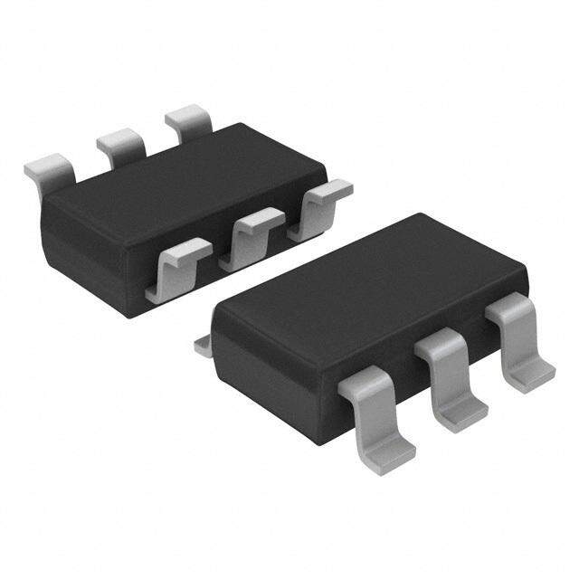
| 产品图片 |
|
| rohs | 符合RoHS无铅 / 符合限制有害物质指令(RoHS)规范要求 |
| 产品系列 | LED照明电子器件,LED照明驱动器,Fairchild Semiconductor FAN5702UMP15X- |
| 数据手册 | |
| 产品型号 | FAN5702UMP15X |
| 产品种类 | LED照明驱动器 |
| 供应商器件封装 | 16-UMLP(1.8x2.6) |
| 其它名称 | FAN5702UMP15XDKR |
| 内部驱动器 | 是 |
| 包装 | Digi-Reel® |
| 单位重量 | 177 mg |
| 商标 | Fairchild Semiconductor |
| 安装类型 | 表面贴装 |
| 安装风格 | SMD/SMT |
| 封装 | Reel |
| 封装/外壳 | 16-UMLP |
| 封装/箱体 | UMLP-16 |
| 工作温度 | -40°C ~ 85°C |
| 工厂包装数量 | 3000 |
| 恒压 | - |
| 恒流 | - |
| 拓扑 | PWM,切换式电容器(充电泵) |
| 最大工作温度 | + 85 C |
| 最小工作温度 | - 40 C |
| 标准包装 | 1 |
| 电压-电源 | 2.7 V ~ 5.5 V |
| 电压-输出 | 2 V ~ 4 V |
| 类型-初级 | 背光 |
| 类型-次级 | 白色 LED |
| 系列 | FAN5702 |
| 输入电压 | 2.7 V to 5.5 V |
| 输出数 | 6 |
| 频率 | 900kHz ~ 1.5MHz |
| 高电平输出电流 | 180 mA |


- 商务部:美国ITC正式对集成电路等产品启动337调查
- 曝三星4nm工艺存在良率问题 高通将骁龙8 Gen1或转产台积电
- 太阳诱电将投资9.5亿元在常州建新厂生产MLCC 预计2023年完工
- 英特尔发布欧洲新工厂建设计划 深化IDM 2.0 战略
- 台积电先进制程称霸业界 有大客户加持明年业绩稳了
- 达到5530亿美元!SIA预计今年全球半导体销售额将创下新高
- 英特尔拟将自动驾驶子公司Mobileye上市 估值或超500亿美元
- 三星加码芯片和SET,合并消费电子和移动部门,撤换高东真等 CEO
- 三星电子宣布重大人事变动 还合并消费电子和移动部门
- 海关总署:前11个月进口集成电路产品价值2.52万亿元 增长14.8%


PDF Datasheet 数据手册内容提取
Is Now Part of To learn more about ON Semiconductor, please visit our website at www.onsemi.com Please note: As part of the Fairchild Semiconductor integration, some of the Fairchild orderable part numbers will need to change in order to meet ON Semiconductor’s system requirements. Since the ON Semiconductor product management systems do not have the ability to manage part nomenclature that utilizes an underscore (_), the underscore (_) in the Fairchild part numbers will be changed to a dash (-). This document may contain device numbers with an underscore (_). Please check the ON Semiconductor website to verify the updated device numbers. The most current and up-to-date ordering information can be found at www.onsemi.com. Please email any questions regarding the system integration to Fairchild_questions@onsemi.com. ON Semiconductor and the ON Semiconductor logo are trademarks of Semiconductor Components Industries, LLC dba ON Semiconductor or its subsidiaries in the United States and/or other countries. ON Semiconductor owns the rights to a number of patents, trademarks, copyrights, trade secrets, and other intellectual property. A listing of ON Semiconductor’s product/patent coverage may be accessed at www.onsemi.com/site/pdf/Patent-Marking.pdf. ON Semiconductor reserves the right to make changes without further notice to any products herein. ON Semiconductor makes no warranty, representation or guarantee regarding the suitability of its products for any particular purpose, nor does ON Semiconductor assume any liability arising out of the application or use of any product or circuit, and specifically disclaims any and all liability, including without limitation special, consequential or incidental damages. Buyer is responsible for its products and applications using ON Semiconductor products, including compliance with all laws, regulations and safety requirements or standards, regardless of any support or applications information provided by ON Semiconductor. “Typical” parameters which may be provided in ON Semiconductor data sheets and/or specifications can and do vary in different applications and actual performance may vary over time. All operating parameters, including “Typicals” must be validated for each customer application by customer’s technical experts. ON Semiconductor does not convey any license under its patent rights nor the rights of others. ON Semiconductor products are not designed, intended, or authorized for use as a critical component in life support systems or any FDA Class 3 medical devices or medical devices with a same or similar classification in a foreign jurisdiction or any devices intended for implantation in the human body. Should Buyer purchase or use ON Semiconductor products for any such unintended or unauthorized application, Buyer shall indemnify and hold ON Semiconductor and its officers, employees, subsidiaries, affiliates, and distributors harmless against all claims, costs, damages, and expenses, and reasonable attorney fees arising out of, directly or indirectly, any claim of personal injury or death associated with such unintended or unauthorized use, even if such claim alleges that ON Semiconductor was negligent regarding the design or manufacture of the part. ON Semiconductor is an Equal Opportunity/Affirmative Action Employer. This literature is subject to all applicable copyright laws and is not for resale in any manner.
F A N 5 7 0 May 2016 2 — C o FAN5702 n f i 2 g Configurable 180 mA 6-LED Driver with I C Control u r a b l e 1 Features Description 8 0 Six (6) Parallel LEDs (up to 30 mA Each) The FAN5702 is a highly integrated and configurable charge- m pump-based multi-LED driver. The device can drive up to six A Total Package Load Current Capability: 180 mA LEDs in parallel with a total output current of 180 mA. 6 - Group from 2 to 6 LEDs for Flexible Backlighting Regulated internal current sinks deliver excellent current and L E brightness matching to all LEDs. I2C Interface for Easy Programming D The FAN5702 has an I2C interface that allows the user to D >600:1 Dimming Ratio for 100 Hz PWM Frequency independently control the brightness with a default grouping r i v Logarithmically Controlled Dimming with 64 Steps of 2,1,1,1,1 for a maximum of five independent lighting e channels. The LED driver can be programmed in a multitude r Secondary Brightness Control Using PWM Dimming of configurations to address broad lighting requirements for w up to 20 kHz in Conjunction with I2C Dimming different platforms. Each LED can be configured through I2C it h Dynamic Backlight Control (DBC) to Reduce Current as five independent channels (Group A has two LEDs by I 2 Consumption default) or any additional LEDs can join Group A to increase C Up to 92% Efficiency the backlighting needs as the display size increases. The C device offers a second dimming control using the EN/PWM o Built-in 1.5x Charge Pump with Low Drop-Out Bypass pin. Applying a PWM dimming signal to this pin allows n t Switch and automatic switching to 1x mode control of the dimming of Group A LEDs so that the average ro current is the linear value multiplied by the PWM dimming l 1.2 MHz Switching Frequency for Small-Sized duty-cycle. Capacitors The device provides excellent efficiency, without an inductor, 16-Bump 1.6 mm x 1.6 mm WLCSP (0.6 mm Height) by operating the charge pump in 1.5x or pass-through mode. 16-Lead 3.0 mm x 3.0 mm UMLP (0.55 mm Height) The FAN5702 can be ordered with default I values of SET 30 mA, 20 mA, 15 mA, or 8 mA. The default I is always SET Applications determined by the I ordered (see Ordering Information). SET LCD Backlighting Mobile Handsets / Smartphones Portable Media Players Ordering Information LED Current Temperature Part Number Package Packing (I ) Range SET FAN5702UC30X 30 mA FAN5702UC20X 20 mA WLCSP-16, 0.4 mm Pitch Tape and Reel FAN5702UC15X 15 mA FAN5702UC08X 8 mA -40 to 85°C FAN5702UMP30X 30 mA FAN5702UMP20X 20 mA UMLP-16, 3.0 x 3.0 x 0.55 mm Tape and Reel FAN5702UMP15X 15 mA FAN5702UMP08X 8 mA © 2010 Fairchild Semiconductor Corporation www.fairchildsemi.com FAN5702 • Rev. 1.8
F A N 5 Typical Application 7 0 2 — C C1+ VOUT o n 1F C f 1F OUT i C1– g u r C2+ CHARGE D1A a G b PUMP 1F C2– D2A ROU le 1 P 8 VIN C A 0 1F GND URR D3 exp mA E an 6 NT D4 da -L EN / S ble E PWM INK D5 to 6 D D SDA LOGIC AND S LE ri CONTROL D6 Ds ve SCL r w i t h I 2 C Figure 1. Typical Application C o n t r o l © 2010 Fairchild Semiconductor Corporation www.fairchildsemi.com FAN5702 • Rev. 1.8 2
F A N 5 WLCSP Pin Configuration 7 0 2 — C o A1 A2 A3 A4 A4 A3 A2 A1 n f i g u r a b B1 B2 B3 B4 B4 B3 B2 B1 l e 1 8 0 m C1 C2 C3 C4 C4 C3 C2 C1 A 6 - L E D1 D2 D3 D4 D4 D3 D2 D1 D D r iv Bumps Facing Down Bumps Facing Up e r w Figure 2. WLCSP-16, 0.4 mm Pitch, 1.61 x 1.61 mm i t h I 2 C Pin Definitions C o n Pin # Name Description t r o D2 VIN Input Supply Voltage. Connect to 2.7 – 5.5 V input power source. DC l B4 GND Ground D1 VOUT Charge Pump Output Voltage. Connect to LED anodes. D3 ,D4 C1+, C1– Charge pump flying capacitor #1 C3, C4 C2+, C2– Charge pump flying capacitor #2 A1,A2 D2A, D1A B1,B2 D4,D3 LED Outputs C1,C2 D6,D5 Enable / PWM dimming input. By default, this pin acts as a simple enable / disable function. When this pin is HIGH, normal operation is enabled. When LOW, the IC is reset and all functions A4 EN / PWM (including I2C communications) are disabled. By setting General Purpose register bit 7 = 1, the pin functions as a PWM dimming input for Group A. To restore the Enable function, the General Purpose register bit 7 must be set LOW. B3 SDA I2C interface serial data A3 SCL I2C interface serial clock © 2010 Fairchild Semiconductor Corporation www.fairchildsemi.com FAN5702 • Rev. 1.8 3
F A N UMLP Pin Configuration 5 7 0 5 8 2 — C o 9 n 4 f i g u r a b l e 1 8 0 1 12 m A 6 - L E D 16 13 D Bottom View r i v Figure 3. UMLP-16, 0.5 mm Pitch, 3 mm x 3 mm e r w i t h Pin Definitions I 2 C Pin # Name Description C o 11 VIN Input Supply Voltage. Connect to 2.7 – 5.5 VDC input power source. n t 6 GND Ground r o l 12 VOUT Charge Pump Output Voltage. Connect to LED anodes. 10,9 C1+, C1– Charge pump flying capacitor #1 8,7 C2+, C2– Charge pump flying capacitor #2 1, 2 D2A, D1A 15, 16 D4,D3 LED Outputs 13, 14 D6,D5 Enable / PWM dimming input. By default, this pin acts as a simple enable / disable function. When this pin is HIGH, normal operation is enabled. When LOW, the IC is reset and all functions 4 EN / PWM (including I2C communications) are disabled. By setting General Purpose register bit 7 = 1, the pin functions as a PWM dimming input for Group A. To restore the Enable function, the General Purpose register bit 7 must be set LOW. 5 SDA I2C interface serial data 3 SCL I2C interface serial clock © 2010 Fairchild Semiconductor Corporation www.fairchildsemi.com FAN5702 • Rev. 1.8 4
F A N 5 Absolute Maximum Ratings 7 0 2 Stresses exceeding the absolute maximum ratings may damage the device. The device may not function or be operable above — the recommended operating conditions and stressing the parts to these levels is not recommended. In addition, extended exposure to stresses above the recommended operating conditions may affect device reliability. The absolute maximum C ratings are stress ratings only. o n f Symbol Parameter Min. Max. Unit ig u VIN, VOUT Pins –0.3 6.0 V r a VCC Other Pins(1) –0.3 VIN + 0.3 V ble Electrostatic Discharge Human Body Model per JESD22-A114 3 1 ESD kV 8 Protection Level Charged Device Model per JESD22-C101 2 0 m T Junction Temperature –40 +150 °C J A TSTG Storage Temperature –65 +150 °C 6 - T Lead Soldering Temperature, 10 Seconds +260 °C L L E Note: D 1. Lesser of V + 0.3 or 6.0 V. D IN r i v e r w Recommended Operating Conditions it h I The Recommended Operating Conditions table defines the conditions for actual device operation. Recommended operating 2 C conditions are specified to ensure optimal performance to the datasheet specifications. Fairchild does not recommend C exceeding them or designing to absolute maximum ratings. o n Symbol Parameter Min. Max. Unit tr o VIN Supply Voltage 2.7 5.5 V l V LED Forward Voltage 2 4 V LED T Ambient Temperature –40 +85 °C A T Junction Temperature –40 +125 °C J Thermal Properties Symbol Parameter Min. Typ. Max. Unit WLCSP 80 Θ Junction-to-Ambient Thermal Resistance °C/W JA UMLP 49 Note: 2. Junction-to-ambient thermal resistance is a function of application and board layout. This data is measured with four-layer 2s2p boards in accordance to JESD51-7 JEDEC standard. Special attention must be paid not to exceed junction temperature T at a given ambient temperate T . J(max) A © 2010 Fairchild Semiconductor Corporation www.fairchildsemi.com FAN5702 • Rev. 1.8 5
F A N 5 Electrical Specifications 7 0 2 Unless otherwise specified: VIN = 2.7 V to 5.5 V; TA = -40C to +85C; and ENA, EN3, EN4, EN5, and EN6 = 1. Typical values are — V = 3.6 V, T = 25C, I = 20 mA, and LED cathode terminals = 0.4 V. Circuit and components are according to Figure 1. IN A LED C Symbol Parameter Conditions Min. Typ. Max. Unit o n f Power Supplies and Thermal Protection i g u 1.5x Mode, No LEDs 4.4 r IQ Quiescent Supply Current mA a 1x Mode, No LEDs 0.3 b l e ISD Shutdown Supply Current EN = 0, VIN = 4.5V, TA = -40C to +85C 0.1 2.0 µA 1 8 Under-Voltage Lockout VIN Rising 2.55 2.70 0 VUVLO Threshold V Falling 2.20 2.40 V m IN A Under-Voltage Lockout VUVHYST Hysteresis 150 mV 6- L T Thermal Shutdown 150 °C E LIMIT D THYST Thermal Shutdown Hysteresis 20 °C D LED Current Sinks r i v ILED Absolute Current Accuracy VCATHODE = 0.4 V; see options for ISET –10% ISET +10% mA er ILED(MAX) Maximum Diode Current(3) ILED = ISET 30 mA wi t I LED Current Matching(4) V = 0.4 V, I = I 0.4 3.0 % h LED_MATCH CATHODE LED SET I 1x to 1.5x Gain Transition C2 V LED Cathode Voltage Falling 100 mV DTH Threshold C V Current Sink Headroom(5) I = 90% I 65 mV o HR LED LED(NOMINAL) n PWM Dimming tr o fPWM PWM Switching Frequency tON_LED(MINIMUM) = 15 µs 20 kHz l D PWM Duty-Cycle f = 100 Hz 0.15 100.00 % PWM PWM Charge Pump 1.5x Mode 2.4 R Output Resistance Ω OUT 1x Mode 0.9 f Switching Frequency 0.9 1.2 1.5 MHz SW t Startup Time V = 90% of V 250 µs START OUT IN Logic Inputs (EN, SDA, SCL) V HIGH-Level Input Voltage 1.2 V IH V LOW-Level Input Voltage 0.4 V IL V Maximum Input Voltage 1.8 5.5 V IMAX I Input Bias Current Input Tied to GND or V 0.01 1.00 µA IN IN Notes: 3. The maximum total output current for the IC should be limited to 180 mA. The total output current can be split between the two groups (IDxA = IDxB = 30 mA maximum). Under maximum output current conditions, special attention must be given to input voltage and LED forward voltage to ensure proper current regulation. See the Maximum Output Current section of the datasheet for more information. 4. For the two groups of current sinks on a part (group A and group B), the following are determined: the maximum sink current in the group (MAX), the minimum sink current in the group (MIN), and the average sink current of the group (AVG). For each group, two matching numbers are calculated: (MAX-AVG)/AVG and (AVG-MIN)/AVG. The largest number of the two (worst case) is considered the matching value for the group. The matching value for a given part is considered to be the highest matching value of the two groups. The typical specification provided is the most likely norm of the matching value for all parts. 5. For each Dxx pin, headroom voltage is the voltage across the internal current sink connected to that pin. V = V - HRx OUT V . If headroom voltage requirement is not met, LED current regulation is compromised. LED © 2010 Fairchild Semiconductor Corporation www.fairchildsemi.com FAN5702 • Rev. 1.8 6
F A N Typical Characteristics 5 7 0 VIN = 3.6 V, TA = 25C, ILED = 20 mA, and LED cathode terminals = 0.4 V. 2 — C o n f i g u r a b l e 1 8 0 m A 6 - L E D D Figure 4. Efficiency with LED Current of 8 mA and Figure 5. LED Current Match for all 6 LED r i v 20 mA Channels at ILED=20 mA e r w i t h I 2 C C o n t r o l Figure 6. LED Current Variation vs. Temperature Figure 7. Shutdown Current vs. Input Voltage Figure 8. Switching Frequency Over-Temperature with LED Current at 20 mA © 2010 Fairchild Semiconductor Corporation www.fairchildsemi.com FAN5702 • Rev. 1.8 7
F A Typical Characteristics N 5 7 VIN = 3.6 V, TA = 25C, ILED = 20 mA, and LED cathode terminals = 0.4 V. 0 2 — C o n f i g u r a b l e 1 8 0 m A 6 - L E Figure 9. Mode Transition from 1x to 1.5x Mode Figure 10. Mode Transition from 1.5x to 1x Mode D Using PWM Control (V Ramp Up) at 2% Using PWM Control (V Ramp Down) at 2% D CATHODE CATHODE Duty Cycle Duty Cycle ri v e r w i t h I 2 C C o n t r o l Figure 11. Line Transient Response in 1x Mode, Figure 12. Line Transient Response in 1.5x Mode, V =3.6 V – 4.2 V, I =20 mA V =2.7 V – 3.3 V, I =20 mA IN LEDx IN LED Figure 13. Line Transient from 1x to 1.5x Mode, Figure 14. Soft-Start with SDA and SCL V =3.2 V – 4.1 V, I =20 mA IN LEDx © 2010 Fairchild Semiconductor Corporation www.fairchildsemi.com FAN5702 • Rev. 1.8 8
F A N 5 Typical Characteristics 7 0 2 — C o n f i g u r a b l e 1 8 0 m A 6 - L E D D Figure 15. Linear Dimming via I2C Interface, Figure 16. PWM Dimming, VIN=3.6 V, ILEDx=20 mA, ri V =3.6 V, I =20 mA, and t =6.4 ms and EN=1 kHz with 20% Duty Cycle v IN LEDx RAMP e r w i t h I 2 C C o n t r o l Figure 17. PWM and Linear (via I2C) Dimming, V =3.6 V, I =20 mA, and EN=1 kHz with 20% IN LEDx Duty Cycle © 2010 Fairchild Semiconductor Corporation www.fairchildsemi.com FAN5702 • Rev. 1.8 9
F A N I2C Timing Specifications 5 7 0 Guaranteed by design. 2 — Symbol Parameter Conditions Min. Typ. Max. Unit C Standard Mode 100 o f SCL Clock Frequency kHz n SCL Fast Mode 400 f i g Standard mode 4.7 u t Bus-Free Time between STOP and START Conditions µs r BUF a Fast Mode 1.3 b l Standard Mode 4 µs e tHD;STA START or Repeated START Hold Time 1 Fast Mode 600 ns 8 0 Standard Mode 4.7 µs m t SCL LOW Period LOW Fast Mode 1.3 ns A 6 Standard Mode 4 µs - t SCL HIGH Period L HIGH Fast Mode 600 ns E D Standard Mode 4.7 µs D t Repeated START Setup Time SU;STA Fast Mode 600.0 ns ri v Standard Mode 250 ns e r tSU;DAT Data Setup Time w Fast Mode 100 ns i t Standard Mode 0 3.45 µs h tHD;DAT Data Hold Time Fast Mode 0 900.00 ns IC2 Standard Mode 20+0.1C 1000 ns C B tRCL SCL Rise Time o Fast Mode 20+0.1CB 300 ns n t Standard Mode 20+0.1CB 300 ns ro tFCL SCL Fall Time Fast Mode 20+0.1CB 300 ns l Standard Mode 20+0.1C 1000 ns B t SDA Rise Time(6) RDA Fast Mode 20+0.1C 300 ns B Standard Mode 20+0.1C 300 ns B t SDA Fall Time FDA Fast Mode 20+0.1C 300 ns B Standard Mode 4 µs t Stop Condition Setup Time SU;STO Fast Mode 600 ns C Capacitive Load for SDA and SCL 400 pF B Note: 6. Rise time of SCL after a repeated START condition and after an ACK bit. Timing Diagram t t F SU;STA t BUF SDA t R T SU;DAT t t HD;STO SCL t HIGH LOW t t HD;STA HD;DAT t HD;STA REPEATED START START STOP START Figure 18. I2C Interface Timing for Fast and Slow Modes © 2010 Fairchild Semiconductor Corporation www.fairchildsemi.com FAN5702 • Rev. 1.8 10
F A Circuit Description N 5 7 The FAN5702 is a white LED driver system based on an Register Controlled Brightness 0 adaptive 1.5x charge pump capable of supplying up to 2 180 mA of total output current. The tightly matched current The DC value of the LED current is modulated according to — the values in Table 1. Current is expressed as a percentage sinks ensure uniform brightness between the LEDs. Each of the full scale current and is illustrated with a 20 mA I . C LED has a common anode configuration with its peak drive SET o current set during manufacturing (see Ordering Information Table 1. Brightness Control n abnridg hItSnEeTs).s Awni thI2inC -cthoem pinadtiibvlied uianlt ecrfuarcree nits suinseksd taos vwareyl l thaes Dimming 0C0o0d0e00 ( Bx5-Bx0) Cur0re.1n2t5 L%e vel ILED (mA)0 (.0IS2E5T= 20 mA) figu r configure the grouping. Each LED is controlled with 64 000001 0.188% 0.038 a exponentially spaced analog brightness control levels 000010 0.249% 0.050 b through I2C, as indicated in Table 1. For maximum flexibility, 000011 0.312% 0.063 le 000100 0.374% 0.075 1 the FAN5702 can be programmed with five independently 000101 0.438% 0.088 8 controlled LED banks; by default, arranged as 2,1,1,1,1 (first 000110 0.499% 0.100 0 two LEDs represent Group A). Through I2C, the device can 000111 0.560% 0.113 m 001000 0.622% 0.125 be reconfigured to add up to six LEDs to Group A as needed 001001 0.692% 0.138 A by application requirements. 001010 0.750% 0.150 6 001011 0.810% 0.163 - L Charge Pump 001100 0.875% 0.175 E 001101 0.938% 0.188 D The charge pump operates in either 1x mode, where V is 001110 1.004% 0.200 OUT connected to V through a bypass switch, or in 1.5x mode. 001111 1.124% 0.225 D IN 010000 1.250% 0.250 r The circuit operates in 1x mode until the LED with the 010001 1.375% 0.275 iv highest forward voltage (VLED(MAX)) can no longer maintain 010010 1.499% 0.300 e current regulation. At that point, 1.5x Mode begins. If the 010011 1.625% 0.325 r 010100 1.750% 0.350 w lowest active cathode voltage is greater than 1.8 V, the 010101 1.881% 0.375 it charge pump switches back to 1x Mode. 010110 2.063% 0.413 h 010111 2.249% 0.450 I IC Enable 011000 2.438% 0.488 C2 011001 2.687% 0.538 By default the General Purpose register bit 7 = 0, the EN pin 011010 2.939% 0.588 C functions as enable/disable. When the EN pin is LOW, all 011011 3.186% 0.638 o circuit functions, including I2C, are disabled and the registers 011100 3.562% 0.713 nt 011101 3.936% 0.788 r are set to their default values. 011110 4.310% 0.863 o l 011111 4.813% 0.963 When the EN pin HIGH, I2C interface is enabled. The LEDs 100000 5.314% 1.063 can be turned on/off by writing to the General Purpose 100001 5.936% 1.188 register. The user can always communicate via I2C with the 100010 6.565% 1.313 100011 7.313% 1.463 device to change register settings regardless of whether any 100100 8.059% 1.613 LED is on or off. 100101 8.938% 1.788 100110 9.876% 1.975 PWM Dimming 100111 10.874% 2.175 101000 12.005% 2.400 By programming the General Purpose register bit 7 = 1, the 101001 13.253% 2.650 EN pin is reappropriated to a PWM dimming input. Applying 101010 14.618% 2.925 101011 16.124% 3.225 a PWM signal to this pin controls the LED current waveform 101100 17.881% 3.575 to be ON when the PWM dimming pin is HIGH and OFF 101101 19.875% 3.975 when the PWM dimming pin is LOW. By using this pin in 101110 22.121% 4.425 conjunction with the I2C register dimming, the part can 101111 24.621% 4.925 110000 27.376% 5.475 achieve higher dimming resolution. For instance, an 8-bit 110001 30.373% 6.075 PWM dimming signal applied along with the 6-bit register 110010 33.623% 6.725 dimming yields better than 14 bits of resolution 110011 37.124% 7.425 110100 40.873% 8.175 110101 44.875% 8.975 To change the PWM dimming pin back to the EN function, 110110 49.124% 9.825 set the General Purpose register bit 7 to 0. 110111 53.624% 10.725 111000 58.375% 11.675 111001 63.378% 12.675 111010 68.625% 13.725 111011 74.122% 14.825 111100 79.874% 15.975 111101 85.873% 17.175 111110 92.373% 18.475 111111 100.000% 20.000 © 2010 Fairchild Semiconductor Corporation www.fairchildsemi.com FAN5702 • Rev. 1.8 11
F A Brightness Ramp Control N Register Addressing 5 When changing the group A brightness, the IC steps through 7 The FAN5702 has six user-accessible registers. 0 the brightness table at rate programmed by the RAMP 2 register, indicated in Table 2. Table 4. I2C Register Addresses — Table 2. Group A Brightness Ramp Control Default Value Address C o RAMP[1:0] Time per Step Full-Scale Ramp Time n 7 6 5 4 3 2 1 0 HEX f i g 00 0.1 ms 6.4 ms GENERAL 0 0 0 0 0 0 0 0 10 u r 01 25 ms 1600 ms CONFIG 0 0 0 0 0 0 0 0 20 a b 10 50 ms 3200 ms l CHA 1 1 1 1 1 1 1 1 A0 e 11 100 ms 6400 ms CH3 1 1 1 1 1 1 1 1 30 18 0 VOUT Short-Circuit Protection CH4 1 1 1 1 1 1 1 1 40 m The FAN5702 has integrated protection circuitry to prevent CH5 1 1 1 1 1 1 1 1 50 A the device from being short circuited when the output voltage CH6 1 1 1 1 1 1 1 1 60 6 - falls below 2 V. If this occurs, FAN5702 turns off the charge L pump and the LED driver outputs, but a small bypass switch Note: E D is left on. The device monitors the output voltage to 7. Bold identifies bits that cannot be overwritten. D determine if it is still in short circuit condition and, once it has Bus Timing r passed, soft-starts and returns to normal operation. iv As shown in Figure 19 data is normally transferred when e V Over-Voltage Protection r OUT SCL is LOW. Data is clocked in to the FAN5702 on the rising w If the output voltage goes above 6 V, the FAN5702 shuts edge of SCL. Typically, data transitions shortly at or after the i t down until this condition has passed. The charge pump and falling edge of SCL to allow ample time for the data to set up h LED driver outputs are turned off. Once this condition has before the next SCL rising edge. I2 C passed, the FAN5702 soft-starts into normal operation. Data change allowed C I2C Interface o n The FAN5702’s serial interface is compatible with standard SDA t r and fast I2C bus specifications. The FAN5702’s SCL line is o an input and its SDA line is a bi-directional open-drain TH l output, meaning that it can only pull down the bus when SCL TSU active. The SDA line only pulls LOW during data reads and when signaling ACK. All data is shifted in MSB (bit 7) first. Figure 19. Data Transfer Timing Slave Address The FAN5702’s slave address is 6CH. Each bus transaction begins and ends with SDA and SCL Table 3. I2C Slave Address HIGH. A transaction begins with a START condition, which is 7 6 5 4 3 2 1 0 defined as SDA transitioning from 1 to 0 with SCL HIGH, as shown in Figure 20. 0 1 1 0 1 1 0 R/W SDA THD;STA Slave Address MS Bit SCL Figure 20. Start Bit © 2010 Fairchild Semiconductor Corporation www.fairchildsemi.com FAN5702 • Rev. 1.8 12
F A A transaction ends with a STOP condition, which is defined During a read from the FAN5702 (Figure 24, the master N as SDA transitioning from 0 to 1 with SCL HIGH, as shown issues a “Repeated Start” after sending the register address 5 7 in Figure 21. and before resending the slave address. The “Repeated 0 2 Start” is a 1-to-0 transition on SDA while SCL is HIGH, as Slave Releases Master Drives — t shown in Figure 22. HD;STO C SDA ANCAKC(K0)( 1o)r Slave Releases tSU;STA tHD;STA o n ACK(0) or SLADDR SDA NACK(1) MS Bit fi g u SCL r SCL a b Figure 21. Stop Bit le Figure 22. Repeated Start Timing 1 8 0 m A 6 - L Read and Write Transactions E D The following figures outline the sequences for data read and write. Bus control is signified by the shading of the packet, D defined as Master Drives Bus and Slave Drives Bus . All addresses and data are MSB first. riv e Table 5. I2C bit Definitions for Figure 23 and Figure 24. r w Symbol Definition it h S START. See Figure 20. I2 C A ACK. The slave drives SDA to 0 to acknowledge the preceding packet. C o A NACK. The slave sends a 1 to NACK the preceding packet. n t R Repeated START. See Figure 22 ro l P STOP. See Figure 21. 7 bits 0 8 bits 0 8 bits 0 S Slave Address 0 A Reg Addr A Data A P Figure 23. Write Transaction 7 bits 0 8 bits 0 7 bits 0 8 bits 1 S Slave Address 0 A Reg Addr A R Slave Address 1 A Data A P Figure 24. Read Transaction © 2010 Fairchild Semiconductor Corporation www.fairchildsemi.com FAN5702 • Rev. 1.8 13
F A Register Descriptions N 5 The following tables define the operation of each register bit. Bold values are power-up defaults. These values apply only to 7 0 I2C version of the part. 2 — Bit Name Default Value Description C GENERAL Default: 00H General Purpose Register ADDR = 10H o 0 Setting this bit=1 changes the EN pin to function as a PWM dimming input for n 7 PWM f group A LEDs. This bit must be set to zero for the chip to be disabled. ig 6,5 FS1, FS2 00 00=20 mA (default), 01=30 mA, 10=15 mA, 11=8 mA when I2C is used. u r a 4 EN6 0 Default=0 (Off), LED Channel Active=1 b l 3 EN5 0 Default=0 (Off), LED Channel Active=1 e 1 2 EN4 0 Default=0 (Off), LED Channel Active=1 8 0 1 EN3 0 Default=0 (Off), LED Channel Active=1 m 0 ENA 0 Default=0 (Off), LED Channel Active=1 A CONFIG Default: 00H Configuration Register ADDR = 20H 6 - L 7 T56 0 Tie channel 5 and 6 together. Default=0 (Separate). Group 5&6 =1. Both E currents are set by CH5 register. T56 is overwritten by either S5A or S6A. D 0 Tie channel 3 and 4 together. Default=0 (Separate). Group 3&4 =1. Both D 6 T34 r currents are set by the CH3 register. T34 is overwritten by either S3A or S4A. i v 5 S6A 0 CH6 group configuration. Independent=0 (default); part of group A=1. e r 4 S5A 0 CH5 group configuration. Independent=0 (default); part of group A=1. w i t 3 S4A 0 CH4 group configuration. Independent=0 (default); part of group A=1. h 2 S3A 0 CH3 group configuration. Independent=0 (default); part of group A=1. I2 C 1,0 RS1, RS0 00 Sets current ramp rate for group A channels C CHA Default: FFH Group A Brightness Control ADDR = A0H o n 11 Vendor ID bits. These bits can be used to distinguish between vendors via I2C. t 7:6 Reserved Writing to these bits does not change their value. ro l 0 – 63 5:0 Brightness A 6-bit value that controls group A brightness per values in Table 1 00 – 3FH CH3 Default: Channel 3 Brightness Control ADDR=30H 7:6 Reserved 11 Writing to these bits does not change their value. 0 – 63 5:0 Brightness 3 6-bit value that controls channel 3 brightness per values in Table 1 00 – 3FH CH4 Default: FFH Channel 4 Brightness Control ADDR = 40H 7:6 Reserved 11 Writing to these bits does not change their value. 0 – 63 5:0 Brightness 4 6-bit value that controls channel 3 brightness per values in Table 1 00 – 3FH CH5 Default: FFH Channel 5 Brightness Control ADDR = 50H 7:6 Reserved 11 Writing to these bits does not change their value. 0 – 63 5:0 Brightness 5 6-bit value that controls channel 3 brightness per values in Table 1 00 – 3FH CH6 Default: FFH Channel 6 Brightness Control ADDR = 60H 7:6 Reserved 11 Writing to these bits does not change their value. 0 – 63 5:0 Brightness 6 6-bit value that controls channel 3 brightness per values in Table 1 00 – 3FH The table below pertains to the Marketing Outline drawing on the following page… Product-Specific Dimensions Product D E X Y FAN5702UCxx 1.610 mm 1.610 mm 0.205 mm 0.205 mm © 2010 Fairchild Semiconductor Corporation www.fairchildsemi.com FAN5702 • Rev. 1.8 14
3.00 3.00±0.10 A 1.75 B PIN 1 3.00±0.10 1.75 3.00 IDENT TOP VIEW 0.75, 16X 0.30, 16X 0.15±0.05 0.50 0.50±0.05 LAND PATTERN RECOMMENDATION SEATING PLANE C NOTES: 0.025±0.025 SIDE VIEW A. DESIGN CONFORMS TO JEDEC MO-248 B. ALL DIMENSIONS ARE IN MILLIMETERS 1.70±0.05 C. LAND PATTERN RECOMMENDATION FROM PIN 1 1 4 PCB MATRIX IPC LP CALCULATOR (V2009) IDENT D. DRAWING FILENAME: MKT-UMLP16BrevB 16 5 0.50 1.70±0.05 13 8 0.37±0.05 (16X) 12 9 0.25±0.05 (16X) 0.50 0.10 C A B 0.05 C BOTTOM VIEW
None
ON Semiconductor and are trademarks of Semiconductor Components Industries, LLC dba ON Semiconductor or its subsidiaries in the United States and/or other countries. ON Semiconductor owns the rights to a number of patents, trademarks, copyrights, trade secrets, and other intellectual property. A listing of ON Semiconductor’s product/patent coverage may be accessed at www.onsemi.com/site/pdf/Patent−Marking.pdf. ON Semiconductor reserves the right to make changes without further notice to any products herein. ON Semiconductor makes no warranty, representation or guarantee regarding the suitability of its products for any particular purpose, nor does ON Semiconductor assume any liability arising out of the application or use of any product or circuit, and specifically disclaims any and all liability, including without limitation special, consequential or incidental damages. Buyer is responsible for its products and applications using ON Semiconductor products, including compliance with all laws, regulations and safety requirements or standards, regardless of any support or applications information provided by ON Semiconductor. “Typical” parameters which may be provided in ON Semiconductor data sheets and/or specifications can and do vary in different applications and actual performance may vary over time. All operating parameters, including “Typicals” must be validated for each customer application by customer’s technical experts. ON Semiconductor does not convey any license under its patent rights nor the rights of others. ON Semiconductor products are not designed, intended, or authorized for use as a critical component in life support systems or any FDA Class 3 medical devices or medical devices with a same or similar classification in a foreign jurisdiction or any devices intended for implantation in the human body. Should Buyer purchase or use ON Semiconductor products for any such unintended or unauthorized application, Buyer shall indemnify and hold ON Semiconductor and its officers, employees, subsidiaries, affiliates, and distributors harmless against all claims, costs, damages, and expenses, and reasonable attorney fees arising out of, directly or indirectly, any claim of personal injury or death associated with such unintended or unauthorized use, even if such claim alleges that ON Semiconductor was negligent regarding the design or manufacture of the part. ON Semiconductor is an Equal Opportunity/Affirmative Action Employer. This literature is subject to all applicable copyright laws and is not for resale in any manner. PUBLICATION ORDERING INFORMATION LITERATURE FULFILLMENT: N. American Technical Support: 800−282−9855 Toll Free ON Semiconductor Website: www.onsemi.com Literature Distribution Center for ON Semiconductor USA/Canada 19521 E. 32nd Pkwy, Aurora, Colorado 80011 USA Europe, Middle East and Africa Technical Support: Order Literature: http://www.onsemi.com/orderlit Phone: 303−675−2175 or 800−344−3860 Toll Free USA/Canada Phone: 421 33 790 2910 Fax: 303−675−2176 or 800−344−3867 Toll Free USA/Canada Japan Customer Focus Center For additional information, please contact your local Email: orderlit@onsemi.com Phone: 81−3−5817−1050 Sales Representative © Semiconductor Components Industries, LLC www.onsemi.com www.onsemi.com 1