ICGOO在线商城 > 集成电路(IC) > PMIC - LED 驱动器 > TLC5971RGET
 Datasheet下载
- 型号: TLC5971RGET
- 制造商: Texas Instruments
- 库位|库存: xxxx|xxxx
- 要求:
| 数量阶梯 | 香港交货 | 国内含税 |
| +xxxx | $xxxx | ¥xxxx |
查看当月历史价格
查看今年历史价格
TLC5971RGET产品简介:
ICGOO电子元器件商城为您提供TLC5971RGET由Texas Instruments设计生产,在icgoo商城现货销售,并且可以通过原厂、代理商等渠道进行代购。 TLC5971RGET价格参考¥10.85-¥22.12。Texas InstrumentsTLC5971RGET封装/规格:PMIC - LED 驱动器, LED 驱动器 IC 12 输出 线性 移位寄存器 60mA 24-VQFN(4x4)。您可以下载TLC5971RGET参考资料、Datasheet数据手册功能说明书,资料中有TLC5971RGET 详细功能的应用电路图电压和使用方法及教程。
Texas Instruments(德州仪器)的TLC5971RGET是一款高性能、高精度的PMIC(电源管理集成电路)LED驱动器,广泛应用于需要精确控制和高效能的LED照明系统中。该器件的主要应用场景包括:

1. 显示屏与背光应用:
   - TLC5971RGET适用于各种类型的LED显示屏,如广告牌、信息板、舞台背景屏等。它能够提供精确的电流控制,确保每个LED亮度一致,从而提高显示质量。
   - 在智能手机、平板电脑和其他便携式设备的背光模块中,该芯片可以实现高效的亮度调节,延长电池寿命。

2. 汽车照明系统:
   - 用于车内氛围灯、仪表盘背光、尾灯、转向灯等。TLC5971RGET具备良好的温度特性和抗干扰能力,能够在复杂的汽车环境中稳定工作,同时支持多种调光模式,满足不同驾驶场景的需求。

3. 建筑与景观照明:
   - 在建筑物外墙、桥梁、公园等场所的景观照明项目中,TLC5971RGET可以驱动大量LED灯串,通过PWM(脉宽调制)或模拟调光方式实现动态效果,营造出丰富多彩的视觉体验。

4. 工业自动化与指示灯:
   - 工业设备中的状态指示灯、警示灯等场合也适合使用TLC5971RGET。其内置的保护机制(如过流、过温保护)提高了系统的可靠性和安全性。

5. 智能家居与消费电子产品:
   - 智能灯具、可穿戴设备、游戏机等消费类电子产品中,TLC5971RGET可以实现低功耗下的高亮度输出,并且支持多通道独立控制,便于开发人员设计出更具创意的产品。

总之,TLC5971RGET凭借其优异的性能参数和丰富的功能特性,在众多领域内为LED驱动提供了理想的解决方案。
| 参数 | 数值 |
| 产品目录 | 集成电路 (IC)半导体 |
| 描述 | IC LED DVR PWM 16B 12CH 24VQFNLED显示驱动器 12Ch,16B ES-PWM RGB LED Driver |
| 产品分类 | |
| 品牌 | Texas Instruments |
| 产品手册 | http://www.ti.com/lit/gpn/tlc5971 |
| 产品图片 |
|
| rohs | 符合RoHS无铅 / 符合限制有害物质指令(RoHS)规范要求 |
| 产品系列 | 驱动器IC,LED显示驱动器,Texas Instruments TLC5971RGET- |
| 数据手册 | |
| 产品型号 | TLC5971RGET |
| 产品种类 | LED显示驱动器 |
| 低电平输出电流 | 2 mA |
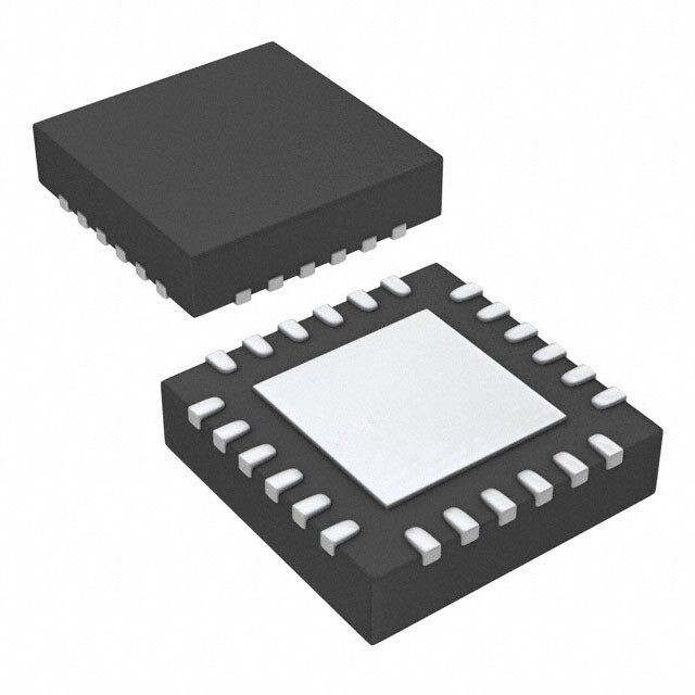
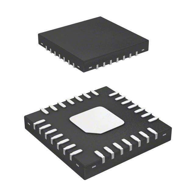
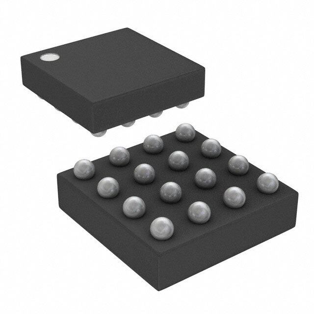
| 供应商器件封装 | 24-VQFN (4x4) |
| 其它名称 | 296-32363-2 |
| 内部驱动器 | 是 |
| 功率耗散 | 3106 mW |
| 包装 | 带卷 (TR) |
| 商标 | Texas Instruments |
| 安装类型 | 表面贴装 |
| 安装风格 | SMD/SMT |
| 封装 | Reel |
| 封装/外壳 | 24-VFQFN 裸露焊盘 |
| 封装/箱体 | VQFN-24 |
| 工作温度 | -40°C ~ 85°C |
| 工厂包装数量 | 250 |
| 恒压 | - |
| 恒流 | 是 |
| 拓扑 | 线性,PWM |
| 最大工作温度 | + 85 C |
| 最大电源电流 | 4 mA |
| 最小工作温度 | - 40 C |
| 标准包装 | 250 |
| 电压-电源 | 3 V ~ 5.5 V,6 V ~ 17 V |
| 电压-输出 | 17V |
| 类型-初级 | 通用 |
| 类型-次级 | 颜色,RGB |
| 系列 | TLC5971 |
| 输出数 | 12 |
| 频率 | 6MHz ~ 12MHz |
| 高电平输出电流 | - 2 mA |


- 商务部:美国ITC正式对集成电路等产品启动337调查
- 曝三星4nm工艺存在良率问题 高通将骁龙8 Gen1或转产台积电
- 太阳诱电将投资9.5亿元在常州建新厂生产MLCC 预计2023年完工
- 英特尔发布欧洲新工厂建设计划 深化IDM 2.0 战略
- 台积电先进制程称霸业界 有大客户加持明年业绩稳了
- 达到5530亿美元!SIA预计今年全球半导体销售额将创下新高
- 英特尔拟将自动驾驶子公司Mobileye上市 估值或超500亿美元
- 三星加码芯片和SET,合并消费电子和移动部门,撤换高东真等 CEO
- 三星电子宣布重大人事变动 还合并消费电子和移动部门
- 海关总署:前11个月进口集成电路产品价值2.52万亿元 增长14.8%


PDF Datasheet 数据手册内容提取
Product Sample & Technical Tools & Support & Folder Buy Documents Software Community TLC5971 SBVS146D–AUGUST2010–REVISEDDECEMBER2015 TLC5971 12-Channel, 16-Bit, Enhanced Spectrum, PWM, RGB, LED Driver With 3.3-V Linear Regulator 1 Features 2 Applications • 12Constant-CurrentSinkOutputChannels RGBLEDClusterLampDisplays 1 • CurrentCapability:60mAPerChannel 3 Description • Grayscale(GS)ControlWithEnhancedSpectrum The TLC5971 device is a 12-channel, constant- PWM: current sink driver. Each output channel has 16-Bit(65536Steps) individually adjustable currents with 65536 PWM • GlobalBrightnessControl(BC): grayscale (GS) steps. Also, each color group can be 7-Bit(128Steps)forEachColorGroup controlled by 128 constant-current sink steps with the • Power-SupplyVoltageRange: global brightness control (BC) function. GS control and BC are accessible through a two-wire signal – InternalLinearRegulator:6Vto17V interface. The maximum current value for each – DirectPowerSupply:3Vto5.5V channel is set by a single external resistor. All • LEDSupplyVoltage:Upto17V constant-current outputs are turned off when the IC is inanovertemperaturecondition. • Constant-CurrentAccuracy: – Channel-to-Channel=±1%(Typical) DeviceInformation(1) – Device-to-Device= ±1%(Typical) PARTNUMBER PACKAGE BODYSIZE(NOM) • DataTransferRate:20MHz HTSSOP(20) 6.50mm×4.40mm TLC5971 • LinearVoltageRegulator:3.3V VQFN(24) 4.00mm×4.00mm • AutoDisplayRepeatFunction (1) For all available packages, see the orderable addendum at • DisplayTimingResetFunction theendofthedatasheet. • InternalandExternalSelectableGSClock • ThermalShutdown(TSD)WithAutoRestart • UnlimitedDeviceCascading • OperatingTemperatureRange:–40°Cto+85°C TypicalApplicationCircuitExample(InternalLinearRegulatorUsingV =6Vto17V) CC VCC Power Supply (6 V to 17 V) GND Device Optional Device Optional GND VCC GND VCC 1mF 1mF VREG OUTR0 VREG OUTR0 IREF OUTG0 IREF OUTG0 ¼ ¼ ¼ ¼ OUTG3 OUTG3 OUTB3 OUTB3 DATA SDTI SDTO SDTI SDTO Controller(1) CLK SCKI SCKO SCKI SCKO GND (1) Theoutputvoltagerangeisfrom0Vto3.3V. NOTE:ThenumberofLEDsinserieschanges,dependingontheVCCvoltage. 1 An IMPORTANT NOTICE at the end of this data sheet addresses availability, warranty, changes, use in safety-critical applications, intellectualpropertymattersandotherimportantdisclaimers.PRODUCTIONDATA.
TLC5971 SBVS146D–AUGUST2010–REVISEDDECEMBER2015 www.ti.com Table of Contents 1 Features.................................................................. 1 8.2 FunctionalBlockDiagram.......................................14 2 Applications........................................................... 1 8.3 FeatureDescription.................................................15 3 Description............................................................. 1 8.4 DeviceFunctionalModes........................................18 8.5 Programming...........................................................19 4 RevisionHistory..................................................... 2 9 ApplicationandImplementation........................ 26 5 PinConfigurationandFunctions......................... 3 9.1 ApplicationInformation............................................26 6 Specifications......................................................... 4 9.2 TypicalApplication..................................................26 6.1 AbsoluteMaximumRatings......................................4 9.3 SystemExamples...................................................31 6.2 ESDRatings..............................................................4 10 PowerSupplyRecommendations..................... 32 6.3 RecommendedOperatingConditions.......................4 11 Layout................................................................... 32 6.4 ThermalInformation..................................................5 6.5 ElectricalCharacteristics...........................................5 11.1 LayoutGuidelines.................................................32 6.6 SwitchingCharacteristics..........................................7 11.2 LayoutExample....................................................32 6.7 DissipationRatings...................................................8 12 DeviceandDocumentationSupport................. 33 6.8 TypicalCharacteristics............................................11 12.1 CommunityResources..........................................33 7 ParametricMeasurementInformation...............13 12.2 Trademarks...........................................................33 7.1 TestCircuits............................................................13 12.3 ElectrostaticDischargeCaution............................33 7.2 PinEquivalentInputandOutputSchematics.........13 12.4 Glossary................................................................33 8 DetailedDescription............................................ 14 13 Mechanical,Packaging,andOrderable Information........................................................... 33 8.1 Overview.................................................................14 4 Revision History NOTE:Pagenumbersforpreviousrevisionsmaydifferfrompagenumbersinthecurrentversion. ChangesfromRevisionC(September2012)toRevisionD Page • AddedPinConfigurationandFunctionssection,ESDRatingstable,FeatureDescriptionsection,DeviceFunctional Modes,ApplicationandImplementationsection,PowerSupplyRecommendationssection,Layoutsection,Device andDocumentationSupportsection,andMechanical,Packaging,andOrderableInformationsection .............................. 1 ChangesfromRevisionB(June2012)toRevisionC Page • Changedtypicalapplicationcircuit(internallinearregulator),addedfootnote1.................................................................... 1 • Changedtypicalapplicationcircuit(directpower),addedfootnote1................................................................................... 31 • Addedtypicalapplicationcircuitexample(directpowersupplyingV =3Vto5.5V,V =15V),addedfootnote1.....31 CC LED ChangesfromRevisionA(December2010)toRevisionB Page • ChangedI parametertestconditionsinElectricalCharacteristicstable.......................................................................... 5 OLKG • UpdatedFigure23................................................................................................................................................................ 15 • Changedbit217descriptioninTable5................................................................................................................................ 24 ChangesfromOriginal(August2010)toRevisionA Page • ChangedGlobalBrightnessControlbulletinFeatures.......................................................................................................... 1 • Changedtypicalapplicationcircuit(internallinearregulator)................................................................................................. 1 • MovedThermalShutdownandNoiseReductionsections................................................................................................... 18 • UpdatedbitnamesforBCR,BCG,andBCBinTable5...................................................................................................... 24 • Changedtypicalapplicationcircuit(directpower)................................................................................................................ 31 2 SubmitDocumentationFeedback Copyright©2010–2015,TexasInstrumentsIncorporated ProductFolderLinks:TLC5971
TLC5971 www.ti.com SBVS146D–AUGUST2010–REVISEDDECEMBER2015 5 Pin Configuration and Functions PWPPackage 20-PinHTSSOP RGEPackage BottomView 24-PinVQFN BottomView IREF 1 20 VREG OUTB1 OUTG1 OUTR1 OUTB0 OUTG0 OUTR0 GND 2 19 VCC 24 23 22 21 20 19 OUTR0 3 18 OUTB3 SDTI 1 18 GND OUTG0 4 17 OUTG3 SCKI 2 17 NC OUTB0 5 PowerPAD 16 OUTR3 NC(1) 3 Thermal Pad 16 IREF OUTR1 6 (Bottom Side) 15 OUTB2 NC 4 (Bottom Side) 15 VREG OUTG1 7 14 OUTG2 SCKO 5 14 NC SDTO 6 13 VCC OUTB1 8 13 OUTR2 SDTI 9 12 SDTO 7 8 9 10 11 12 SCKI 10 11 SCKO OUTR2 OUTG2 OUTB2 OUTR3 OUTG3 OUTB3 NC=notconnected PinFunctions PIN I/O DESCRIPTION NAME PWP RGE SDTI 9 1 I Serialdatainputforthe224-bitshiftregister Serialdatashiftclockinput. DatapresentonSDTIareshiftedtotheLSBofthe224-bitshiftregisterwiththeSCKIrisingedge SCKI 10 2 I DataintheshiftregisterareshiftedtowardtheMSBateachSCKIrisingedge. TheMSBdataoftheshiftregisterappearonSDTO. Serialdataoutputofthe224-bitshiftregister. SDTO 12 6 O SDTOisconnectedtotheMSBofthe224-bitshiftregister. DataareclockedoutattheSCKIrisingedge. Serialdatashiftclockoutput. SCKO 11 5 O TheinputshiftclocksignalfromSCKIisadjustedtothetimingoftheserialdataoutputforSDTO andthesignalisthenoutputatSCKO. Internallinearvoltageregulatoroutput. Adecouplingcapacitorof1µFmustbeconnected.Thisoutputcanbeusedforexternaldevices VREG 20 15 I/O asa3.3-Vpowersupply.ThisterminalcanbeconnectedwiththeVREGterminalofother devicestoincreasethesupplycurrent.Also,thispincanbesuppliedwith3Vto5.5Vfroman externalpowersupplybyconnectingittoVCC. Maximumcurrentprogrammingterminal. AresistorconnectedbetweenIREFandGNDsetsthemaximumcurrentforeveryconstant- IREF 1 16 I/O currentoutput.WhenthisterminalisdirectlyconnectedtoGND,alloutputsareforcedoff.The externalresistorshouldbeplacedclosetothedevice. OUTR0 3 19 O OUTR1 6 22 O REDconstant-currentoutputs. Multipleoutputscanbeconfiguredinparalleltoincreasetheconstant-currentcapability. OUTR2 13 7 O Differentvoltagescanbeappliedtoeachoutput. OUTR3 16 10 O OUTG0 4 20 O OUTG1 7 23 O GREENconstant-currentoutputs. Multipleoutputscanbeconfiguredinparalleltoincreasetheconstant-currentcapability. OUTG2 14 8 O Differentvoltagescanbeappliedtoeachoutput. OUTG3 17 11 O OUTB0 5 21 O OUTB1 8 24 O BLUEconstant-currentoutputs. Multipleoutputscanbeconfiguredinparalleltoincreasetheconstant-currentcapability. OUTB2 15 9 O Differentvoltagescanbeappliedtoeachoutput. OUTB3 18 12 O VCC 19 13 — Power-supplyterminal Copyright©2010–2015,TexasInstrumentsIncorporated SubmitDocumentationFeedback 3 ProductFolderLinks:TLC5971
TLC5971 SBVS146D–AUGUST2010–REVISEDDECEMBER2015 www.ti.com PinFunctions(continued) PIN I/O DESCRIPTION NAME PWP RGE GND, PowerPAD 2 — — (PWP) GND, Powergroundterminal exposed — 18 — thermal pad(RGE) 3,4,14, NC — — Nointernalconnection 17 6 Specifications 6.1 Absolute Maximum Ratings overoperatingfree-airtemperaturerange,unlessotherwisenoted.(1)(2) MIN MAX UNIT Supplyvoltage,VCC –0.3 18 V IREF –0.3 VREG+0.3 V Inputvoltage SDTI,SCKI –0.3 VREG+0.6 V OUTR0toOUTR3,OUTG0toOUTG3,OUTB0toOUTB3 –0.3 18 V Outputvoltage SDTO,SCKO –0.3 VREG+0.3 V VREG –0.3 6 V OUTR0toOUTR3,OUTG0toOUTG3,OUTB0toOUTB3 75 mA Outputcurrent(DC) VREG –30 mA Operatingjunctiontemperature,TJ(max) 150 °C Storagetemperature,Tstg –55 150 °C (1) StressesbeyondthoselistedunderAbsoluteMaximumRatingsmaycausepermanentdamagetothedevice.Thesearestressratings only,andfunctionaloperationofthedeviceattheseoranyotherconditionsbeyondthoseindicatedunderRecommendedOperating Conditionsisnotimplied.Exposuretoabsolute-maximum-ratedconditionsforextendedperiodsmayaffectdevicereliability. (2) Allvoltagevaluesarewithrespecttonetworkgroundterminal. 6.2 ESD Ratings VALUE UNIT Electrostatic Humanbodymodel(HBM),perANSI/ESDA/JEDECJS-001(1) ±4000 V V (ESD) discharge Charged-devicemodel(CDM),perJEDECspecificationJESD22-C101(2) ±2000 (1) JEDECdocumentJEP155statesthat500-VHBMallowssafemanufacturingwithastandardESDcontrolprocess. (2) JEDECdocumentJEP157statesthat250-VCDMallowssafemanufacturingwithastandardESDcontrolprocess. 6.3 Recommended Operating Conditions atT =–40°Cto+85°C,andVCC=6Vto17VorVCC=VREG=3Vto5.5V,unlessotherwisenoted. A MIN NOM MAX UNIT DCCHARACTERISTICS VCC Supplyvoltage,internalvoltageregulatorused 6 17 V VREG Supplyvoltage,VREGconnectedtoVCC 3 3.3 5.5 V Voltageappliedtooutput VO (OUTR0toOUTR3,OUTG0toOUTG3,OUTB0toOUTB3) 17 V VIH High-levelinputvoltage(SDTI,SCKI) 0.7×VREG VREG V VIL Low-levelinputvoltage(SDTI,SCKI) GND 0.3×VREG V VIHYS Inputvoltagehysteresis(SDTI,SCKI) 0.2×VREG V IOH High-leveloutputcurrent(SDTO) –2 mA IOL Low-leveloutputcurrent(SDTO) 2 mA Constantoutputsinkcurrent IOLC (OUTR0toOUTR3,OUTG0toOUTG3,OUTB0toOUTB3) 60 mA 4 SubmitDocumentationFeedback Copyright©2010–2015,TexasInstrumentsIncorporated ProductFolderLinks:TLC5971
TLC5971 www.ti.com SBVS146D–AUGUST2010–REVISEDDECEMBER2015 Recommended Operating Conditions (continued) atT =–40°Cto+85°C,andVCC=6Vto17VorVCC=VREG=3Vto5.5V,unlessotherwisenoted. A MIN NOM MAX UNIT IREG Voltageregulatoroutputcurrent(VREG) –25 mA TA Operatingfreetemperaturerange –40 85 °C TJ Operatingjunctiontemperature –40 125 °C ACCHARACTERISTICS fCLK(SCKI) DataclockfrequencyandGScontrolclockfrequency,SCKI 0.007 20 MHz tWH/tWL Pulseduration,SCKI 10 ns tSU Setuptime,SDTI–SCKI↑ 5 ns tH Holdtime,SDTI–SCKI↑ 3 ns 6.4 Thermal Information TLC5971 THERMALMETRIC(1) PWP(HTSSOP) RGE(VQFN) UNIT 20PINS 24PINS θ Junction-to-ambientthermalresistance 68.6 38 °C/W JA θ Junction-to-case(top)thermalresistance 44.2 40.5 °C/W JCtop θ Junction-to-boardthermalresistance 19.3 10.2 °C/W JB ψ Junction-to-topcharacterizationparameter 2.7 0.3 °C/W JT ψ Junction-to-boardcharacterizationparameter 15.7 10 °C/W JB θ Junction-to-case(bottom)thermalresistance 1.8 2.9 °C/W JCbot (1) Formoreinformationabouttraditionalandnewthermalmetrics,seetheSemiconductorandICPackageThermalMetricsapplication report,SPRA953. 6.5 Electrical Characteristics AtT =–40°Cto+85°C,V =6Vto17VorVCC=VREG=3Vto5.5V,VLED=5V,andC =1µF,unlessotherwise A CC VREG noted.TypicalvaluesareatT =25°CandVCC=12V. A PARAMETER TESTCONDITIONS MIN TYP MAX UNIT VOH High-leveloutputvoltage,SDTO/SCKO IOH=–2mA VREG–0.4 VREG V VOL Low-leveloutputvoltage,SDTO/SCKO IOL=2mA 0 0.4 V II Inputcurrent,SDTI/SCKI VI=VREGorGND –1 1 µA SDTI/SCKI=low,BLANK=1,GSn=FFFFh, ICC BCX=7Fh,VOUTXn=1V,RIREF=24kΩ(IOLCMax=2mA) 2 4 mA SDTI/SCKI=low,BLANK=1,GSn=FFFFh, ICC1 BCX=7Fh,VOUTXn=1V,RIREF=1.6kΩ(IOLCMax=30mA) 6 9 mA Supplycurrent SDTI=10MHz,SCKI=20MHz,BLANK=0, ICC2 autorepeatenable,externalGSclockselected,GSn=FFFFh, 14 22 mA BCX=7Fh,VOUTXn=1V,RIREF=1.6kΩ(IOLCMax=30mA) SDTI=10MHz,SCKI=20MHz,BLANK=0, ICC3 autorepeatenable,externalGSclockselected,GSn=FFFFh, 21 36 mA BCX=7Fh,VOUTXn=1V,RIREF=0.82kΩ(IOLCMax=60mA) IOLC Constantoutputcurrent,OUTXn AVlOlUOTfUixT=X1nVo,nR,BIRCEFX==07.8F2hk,ΩVO(UIOTLXCnM=ax1=V6,0mA) 56.3 60.5 64.7 mA IOLKG Leakageoutputcurrent,OUTXn AVlOlUOTfUixT=X1n7oVff,,RBICREXF==70F.8h2,kVΩOU(TIXOnLC=Ma1x7=V6,0mA) 0.1 µA Copyright©2010–2015,TexasInstrumentsIncorporated SubmitDocumentationFeedback 5 ProductFolderLinks:TLC5971
TLC5971 SBVS146D–AUGUST2010–REVISEDDECEMBER2015 www.ti.com Electrical Characteristics (continued) AtT =–40°Cto+85°C,V =6Vto17VorVCC=VREG=3Vto5.5V,VLED=5V,andC =1µF,unlessotherwise A CC VREG noted.TypicalvaluesareatT =25°CandVCC=12V. A PARAMETER TESTCONDITIONS MIN TYP MAX UNIT Constant-currenterror(1) ΔIOLC (OcUhaTnXnnel-to-channelinsamecolorgroup), ARlIlREOFU=T0X.n82onkΩ,B(CIOXLC=Ma7xF=h6,0VOmUATX)n=VOUTfix=1V, –3% ±1% 3% Constantcurrenterror(2) AllOUTXnon,BCX=7Fh,VOUTXn=VOUTfix=1V, ΔIOLC1 (device-to-deviceinsamecolorgroup), RIREF=0.82kΩ(IOLCMax=60mA),atsamegroupedcoloroutput –4% ±1 4% OUTXn ofOUTR0-3,OUTG0-3,andOUTB0-3 ΔIOLC2 LOiUneTXreng(3u)lationofconstant-currentoutput, ARlIlREOFU=T0n.8o2n,kBΩC(XIOL=CM7aFxh=,V60OUmTXAn)=VOUTfix=1V, –1 ±0.5 1 %/V (1) Thedeviationofeachoutputinthesamecolorgroup(OUTR0-OUTR3orOUTG0-OUTG3orOUTB0-OUTB3) fromtheaveragecurrentfromthesamecolorgroup.DeviationiscalculatedbyEquation1: I D(%) = OLCXn -1 ´100 (I + I + I + I ) OLCX0 OLCX1 OLCX2 OLCX3 4 where (a)X=R/G/B, (b) n=0-3. (1) (2) Thedeviationofeachcolorgroupconstant-currentaveragefromtheidealconstant-currentvalue.Deviationis calculatedbyEquation2: (I + I + I + I ) OLCX0 OLCX1 OLCX2 OLCX3 -(Ideal Output Current) 4 D(%) = ´100 Ideal Output Current where (a)X=R/G/B. (2) IdealcurrentiscalculatedbyEquation3 fortheOUTRnandOUTGngroups: 1.21 I (mA) = 41´ OLCXn(IDEAL) R (W) IREF where (a)X=R/G/B. (3) (3) LineregulationiscalculatedbyEquation4: D(%/V) = (IOLCXnat VCC = 5.5 V)-(IOLCXnat VCC = 3 V) ´ 100 (IOLCXnat VCC = 3 V) 5.5 V-3 V where (a)X=R/G/B, (b) n=0-3. (4) 6 SubmitDocumentationFeedback Copyright©2010–2015,TexasInstrumentsIncorporated ProductFolderLinks:TLC5971
TLC5971 www.ti.com SBVS146D–AUGUST2010–REVISEDDECEMBER2015 Electrical Characteristics (continued) AtT =–40°Cto+85°C,V =6Vto17VorVCC=VREG=3Vto5.5V,VLED=5V,andC =1µF,unlessotherwise A CC VREG noted.TypicalvaluesareatT =25°CandVCC=12V. A PARAMETER TESTCONDITIONS MIN TYP MAX UNIT ΔIOLC3 LOoUaTdXrne(g4u)lationofconstant-currentoutput, ARlIlREOFU=T0n.8o2n,kBΩC(XIOL=CM7aFxh=,V60OUmTXAn)=VOUTfix=1V, –3 ±1 3 %/V TTSD Thermalshutdowntemperature Junctiontemperature(5) 150 165 180 °C THYS Thermalshutdownhysteresis Junctiontemperature(5) 5 10 20 °C VIREF Referencevoltageoutput,IREF RIREF=0.82kΩ 1.18 1.21 1.24 V VREG Linearregulatoroutputvoltage,VREG VCC=6Vto17V,IREG=0mAto–25mA 3.1 3.3 3.5 V ΔVREG Lineregulationoflinearregulator,VREG VCC=6Vto17V,IREG=0mA 90 mV ΔVREG1 Loadregulationoflinearregulator,VREG VCC=12V,IREG=0mAto–25mA 120 mV VSTR Undervoltagelockoutrelease,VREG 2.5 2.7 2.9 V VHYS Undervoltagelockouthysteresis,VREG 300 400 500 mV (4) LoadregulationiscalculatedbyEquation5: D(%/V) = (IOLCXnat VOUTXn= 3 V)-(IOLCXnat VOUTXn= 1 V) ´ 100 (I at V = 1 V) 3 V-1 V OLCXn OUTXn where (a)X=R/G/B, (b) n=0-3. (5) (5) Nottested,specifiedbydesign. 6.6 Switching Characteristics AtT =–40°Cto+85°C,V =6Vto17VorVCC=VREG=3Vto5.5V,C =1µF,C =15pF,R =68Ω,andVLED= A CC VREG L L 5V,unlessotherwisenoted.TypicalvaluesareatT =25°CandVCC=12V. A PARAMETER TESTCONDITIONS MIN TYP MAX UNIT t Risetime,SDTO/SCKO 3 10 ns R0 t Risetime,OUTXn BCX=7Fh 5 15 ns R1 t Falltime,SDTO/SCKO 3 10 ns F0 t Falltime,OUTXn BCX=7Fh 15 25 ns F1 t SCKI↑toSDTO↑↓ 10 25 60 ns D0 t SCKI↑toSCKO↑ 5 15 40 ns D1 t (1) SCKO↑toSDTO↑↓ 5 10 20 ns D2 SCKI↑toOUTRn↑↓,BLANK=0,BCXn= 7Fh,OUTTMG=1 t 10 25 60 ns D3 OrSCKI↓toOUTRn↑↓,BLANK=0, BCXn=7Fh,OUTTMG=0 SCKI↑toOUTGn↑↓,BLANK=0,BCXn Propagationdelay =7Fh,OUTTMG=1 t 25 50 90 ns D4 OrSCKI↓toOUTGn↑↓,BLANK=0, BCXn=7Fh,OUTTMG=0 SCKI↑toOUTBn↑↓,BLANK=0,BCXn= 7Fh,OUTTMG=1 t 40 75 120 ns D5 OrSCKI↓toOUTBn↑↓,BLANK=0, BCXn=7Fh,OUTTMG=0 t (2) LastSCKI↑tointernallatchpulse 8/f 16384/f s D6 genaration OSC OSC t Shiftclockoutputonepulsewidth SCKO↑toSCKO↓ 12 25 35 ns W(SCKO) f Internaloscillatorfrequency 6 10 12 MHz OSC (1) Thepropagationdelaysarecalculatedbyt =t –t . D2 D0 D1 (2) ThegenerationtimingoftheinternallatchpulsechangesdependingontheSCKIclockfrequency;seetheInternalLatchPulse GenerationTimingsection. Copyright©2010–2015,TexasInstrumentsIncorporated SubmitDocumentationFeedback 7 ProductFolderLinks:TLC5971
TLC5971 SBVS146D–AUGUST2010–REVISEDDECEMBER2015 www.ti.com 6.7 Dissipation Ratings DERATINGFACTOR POWERRATING POWERRATING POWERRATING PACKAGE ABOVET =25°C T <25°C T =70°C T =85°C A A A A HTSSOP20-pinwithPowerPADsoldered(1) 25.7mW/°C 3121mW 1998mW 1623mW QFN24-pinexposedthermalpad soldered(2) 24.8mW/°C 3106mW 1988mW 1615mW (1) WithPowerPADsolderedontocopperareaonTIrecommendedprintedcircuitboard(PCB);2-oz.copper.Formoreinformation,see applicationreportPowerPADThermally-EnhancedPackage(SLMA002)availablefordownloadatwww.ti.com. (2) ThepackagethermalimpedanceiscalculatedinaccordancewithJESD51-5. T , T : WH WL VREG SCKI(1) 50% GND T T WH WL T , T : SU H VREG SCKI(1) 50% GND T T SU H VREG SDTI(1) 50% GND (1) Inputpulseriseandfalltimeis1nsto3ns. Figure1. InputTiming t , t , t , t , t , t , t , t , t , t : R0 R1 F0 F1 D0 D1 D2 D3 D4 D5 VREG INPUT(1) 50% GND t D V or V OH OUTXnH 90% OUTPUT 50% 10% V or V OL OUTXnL t or t R F (1) Inputpulseriseandfalltimeis1nsto3ns. Figure2. OutputTiming 8 SubmitDocumentationFeedback Copyright©2010–2015,TexasInstrumentsIncorporated ProductFolderLinks:TLC5971
TLC5971 www.ti.com SBVS146D–AUGUST2010–REVISEDDECEMBER2015 Write Command (6 Bits) Write Data (218 Bits) SDTI DATA WRT WRT WRT DATA DATA DATA DATA WRT WRT WRT WRT WRT WRT DATA DATA DATA 0A CMD5 CMD4 CMD0 217B 2B 1B 0B CMD5 CMD4 CMD3 CMD2 CMD1 CMD0 217C 216C 215C t H tSU tWH SCKI 1 2 6 222 223 224 1 2 3 4 5 6 7 8 9 t WL 224-Bit ShiftRegister DATA WRT WRT WRT DATA DATA DATA DATA WRT WRT WRT WRT WRT WRT DATA DATA LSB (Internal) 0A CMD5 CMD4 CMD0 217B 2B 1B 0B CMD5 CMD4 CMD3 CMD2 CMD1 CMD0 217C 216C 224-Bit Shift Register DATA DATA WRT WRT WRT DATA DATA DATA DATA WRT WRT WRT WRT WRT WRT DATA LSB + 1 (Internal) 1A 0A CMD5 CMD1 CMD0 3B 2B 1B 0B CMD5 CMD4 CMD3 CMD2 CMD1 CMD0 217C ¼ ¼ ¼ ¼ 224-Bit Shift Register WRT WRT WRT DATA DATA DATA WRT WRT WRT WRT WRT WRT DATA DATA DATA DATA MSB-1 (Internal) CMD4 CMD3 CMD2 216A 215A 0A CMD5 CMD4 CMD3 CMD2 CMD1 CMD0 217B 216B 215B 214B 224-Bit ShiftRegister WRT WRT WRT DATA DATA DATA DATA WRT WRT WRT WRT WRT WRT DATA DATA DATA MSB (Internal) CMD5 CMD4 CMD3 217A 216A 1A 0A CMD5 CMD4 CMD3 CMD2 CMD1 CMD0 217B 216B 215B t (2) D6 Latch Signal (Internal) Latch Data Previous Data Latest Data(All GS Data are 0001h) (Internal) 1 BLANK Bit inData Latch (Internal) 0 1 EXTGCK Bit in Data Latch (Internal) 0 1 OUTTMG Bit inData Latch (Internal) 0 t D0 SDTO WRT WRT WRT DATA DATA DATA DATA WRT WRT WRT WRT WRT WRT DATA DATA DATA CMD5 CMD4 CMD3 217A 216A 1A 0A CMD5 CMD4 CMD3 CMD2 CMD1 CMD0 217B 216B 215B t /t t t R0 F0 D1 W(SCKO) SCKO t (V ) F1 OUTXnH OFF OUTR0-R3 (V )(1) ON OUTXnL t R1 (VOUTXnH) tD3 OFF OUTG0-G3 (V )(1) ON OUTXnL t D4 (V ) OUTXnH OFF OUTB0-B3 (V )(1) ON OUTXnL t D5 (1) OUTXnON-OFFtimingdependsonpreviousGSdatainthe218-bitdatalatch. (2) ThepropagationdelaytimeshowstheperiodfromtherisingedgeofthelastSCKI,notthe224thSCKItotheinternal latchsignalgeneration. Figure3. DataWriteandOUTXnSwitchingTiming(OUTTMG=1) Copyright©2010–2015,TexasInstrumentsIncorporated SubmitDocumentationFeedback 9 ProductFolderLinks:TLC5971
TLC5971 SBVS146D–AUGUST2010–REVISEDDECEMBER2015 www.ti.com Write Command (6 Bits) Write Data (218 Bits) SDTI DATA WRT WRT WRT DATA DATA DATA DATA WRT WRT WRT WRT WRT WRT DATA DATA DATA 0A CMD5 CMD4 CMD0 217B 2B 1B 0B CMD5 CMD4 CMD3 CMD2 CMD1 CMD0 217C 216C 215C t H tSU tWH SCKI 1 2 6 222 223 224 1 2 3 4 5 6 7 8 9 t WL 224-Bit ShiftRegister DATA WRT WRT WRT DATA DATA DATA DATA WRT WRT WRT WRT WRT WRT DATA DATA LSB (Internal) 0A CMD5 CMD4 CMD0 217B 2B 1B 0B CMD5 CMD4 CMD3 CMD2 CMD1 CMD0 217C 216C 224-Bit Shift Register DATA DATA WRT WRT WRT DATA DATA DATA DATA WRT WRT WRT WRT WRT WRT DATA LSB + 1 (Internal) 1A 0A CMD5 CMD1 CMD0 3B 2B 1B 0B CMD5 CMD4 CMD3 CMD2 CMD1 CMD0 217C ¼ ¼ ¼ ¼ 224-Bit Shift Register WRT WRT WRT DATA DATA DATA WRT WRT WRT WRT WRT WRT DATA DATA DATA DATA MSB-1 (Internal) CMD4 CMD3 CMD2 216A 215A 0A CMD5 CMD4 CMD3 CMD2 CMD1 CMD0 217B 216B 215B 214B 224-Bit ShiftRegister WRT WRT WRT DATA DATA DATA DATA WRT WRT WRT WRT WRT WRT DATA DATA DATA MSB (Internal) CMD5 CMD4 CMD3 217A 216A 1A 0A CMD5 CMD4 CMD3 CMD2 CMD1 CMD0 217B 216B 215B t (2) D6 Latch Signal (Internal) Latch Data Previous Data Latest Data(All GS Data are 0001h) (Internal) 1 BLANK Bit inData Latch (Internal) 0 1 EXTGCK Bit in Data Latch (Internal) 0 1 OUTTMG Bit inData Latch (Internal) 0 t D0 SDTO WRT WRT WRT DATA DATA DATA DATA WRT WRT WRT WRT WRT WRT DATA DATA DATA CMD5 CMD4 CMD3 217A 216A 1A 0A CMD5 CMD4 CMD3 CMD2 CMD1 CMD0 217B 216B 215B t /t t t R0 F0 D1 W(SCKO) SCKO t (V ) F1 OUTXnH OFF OUTR0-R3 (V )(1) ON OUTXnL t R1 (VOUTXnH) tD3 OFF OUTG0-G3 (V )(1) ON OUTXnL t D4 (V ) OUTXnH OFF OUTB0-B3 (V )(1) ON OUTXnL t D5 (1) OUTXnON-OFFtimingdependsonpreviousGSdatainthe218-bitdatalatch. (2) ThepropagationdelaytimeshowstheperiodfromtherisingedgeofthelastSCKI,notthe224thSCKItotheinternal latchsignalgeneration. Figure4. DataWriteandOUTXnSwitchingTiming(OUTTMG=0) 10 SubmitDocumentationFeedback Copyright©2010–2015,TexasInstrumentsIncorporated ProductFolderLinks:TLC5971
TLC5971 www.ti.com SBVS146D–AUGUST2010–REVISEDDECEMBER2015 6.8 Typical Characteristics AtT =25°CandVCC=24V,unlessotherwisenoted. A 100 4000 W) 24.805 W) Resistor (k 10 9.922 3.307 n Rate (m 3000 R, Reference IREF 1 4.961 2.481 1.19.86454 1.411.72401.100.29920.9020.827 Power Dissipatio 21000000 TLC5971PWP TLC5971RGE 0.1 0 0 10 20 30 40 50 60 70 -40 -20 0 20 40 60 80 100 I , Output Current (mA) Free-Air Temperature (°C) OLC Figure5.ReferenceResistorvsOutputCurrent Figure6.PowerDissipationvsTemperature 70 64 T = +25°C, VCC = 12 V, BCx = 7Fh I = 60 mA A 63 OLCMax 60 VCC = 12 V IOLCMax= 60 mA IOLCMax= 50 mA 62 BCx = 7Fh A) 50 A) 61 m m nt ( 40 IOLCMax= 40 mA nt ( 60 e e ut Curr 30 IOLCMax= 30 mA ut Curr 5598 p I = 20 mA p Out 20 OLCMax Out 57 T =-40°C IOLCMax= 2 mA IOLCMax= 5 mA IOLCMax= 10 mA 56 TA= +25°C 10 A 55 T = +85°C A 0 54 0 0.5 1 1.5 2 2.5 3 0 0.5 1 1.5 2 2.5 3 Output Voltage (V) Output Voltage (V) Figure7.OutputCurrentvsOutputVoltage Figure8.OutputCurrentvsOutputVoltage 3 3 T = +25°C I = 60 mA A OLCMax VCC = 12 V VCC = 12 V 2 2 BCx = 7Fh BCx = 7Fh 1 1 %) %) ( ( C 0 C 0 OL OL DI DI -1 -1 -2 -2 -3 -3 0 10 20 30 40 50 60 -40 -20 0 20 40 60 80 100 Output Current (mA) Ambient Temperature (°C) Figure9.Constant-CurrentErrorvsOutputCurrent Figure10.Constant-CurrentErrorvsAmbientTemperature (Channel-to-ChannelinColorGroup) (Channel-to-ChannelinColorGroup) Copyright©2010–2015,TexasInstrumentsIncorporated SubmitDocumentationFeedback 11 ProductFolderLinks:TLC5971
TLC5971 SBVS146D–AUGUST2010–REVISEDDECEMBER2015 www.ti.com Typical Characteristics (continued) AtT =25°CandVCC=24V,unlessotherwisenoted. A 70 30 T = +25°C T = +25°C, VCC = 12 V A A 60 VCC = 12 V 25 BCx = 7Fh, GSx = FFFFh I = 60 mA EXTGCK = 1, DSPRPT = 1 OLCMax A) 50 SDTI = 10 MHz, SCKI = 20 MHz m 20 ut Current ( 4300 IOLCMax= 2 mA IOLCMax= 30 mA I(mA)CC 15 Outp 20 10 I = 10 mA 10 OLCMax 5 0 0 0 16 32 48 64 80 96 112 128 0 10 20 30 40 50 60 Brightness Control Data (dec) Output Current (mA) Figure11.GlobalBrightnessControlLinearity Figure12.SupplyCurrentvsOutputCurrent 30 V) 3.5 ( G E 3.45 25 VR e, 3.4 g mA) 20 ut Volta 3.35 (CC 15 Outp 3.3 I 10 IOLCMax= 60 mA, VCC = 12 V gulator 3.32.52 TA= +25°C,IOLCMax= 60 mA, 5 BCx = 7Fh, GSx = FFFFh Re VCC = 12 V EXTGCK = 1, DSPRPT = 1 ar 3.15 BCx = 7Fh, GSx = FFFFh SDTI = 10 MHz, SCKI = 20 MHz ne EXTGCK = 0, DSPRPT = 1 0 Li 3.1 -40 -20 0 20 40 60 80 100 0 5 10 15 20 25 Ambient Temperature (°C) Linear Regulator Output Current, I (mA) REG Figure13.SupplyCurrentvsAmbientTemperature Figure14.LinearRegulatorOutputVoltagevsLinear RegulatorOutputCurrent (V)REG 3.34.55 TBAC=x =+ 275F°hC, ,GIOSLxC M=a xF=F F6F0h mA, CH1 (2 V/div) (OCUHTR10) I TA== +6205 m°CA,,V BCCCx == 172F hV, Voltage, V 3.33.54 EXTGCK = 0, DSPRPT = 1 (OCUHTG20) GOLSCXRMnaLx == 60800W1,h O, VULTETDM =G 5= V1, ut CH2 (2 V/div) utp 3.3 IREG= 0 mA O CH3 gulator 3.32.52 IREG=-25 mA CH3 (2 V/div) CH4 (OUTB0) e (SCKI) R ar 3.15 CH4 (5 V/div) e n Li 3.1 Time (20 ns/div) 6 8 10 12 14 16 18 Supply Voltage, V (V) CC Figure15.LinearRegulatorOutputVoltagevsSupply Figure16.Constant-CurrentOutputVoltageWaveform Voltage 12 SubmitDocumentationFeedback Copyright©2010–2015,TexasInstrumentsIncorporated ProductFolderLinks:TLC5971
TLC5971 www.ti.com SBVS146D–AUGUST2010–REVISEDDECEMBER2015 7 Parametric Measurement Information 7.1 Test Circuits VCC R VREG L VCC OUTXn(1) VLED VCC IREF CVREG R GND CL(2) VCC VREG SDTO/SCKO IREF C C(1) VREG GND L (1) X=R/G/B,n=0-3. (2) C includes measurement probe and stray L capacitance. (1) CL includes measurement probe and stray capacitance. Figure17. Rise/FallTimeTestCircuitforOUTXn Figure18. Rise/FallTimeTestCircuitfor SDTO/SCKO VCC OUTR0 VREG ¼ OUTXn(1) VCC ¼ IREF CVREG OUTB3 V R GND OUTXn IREF V OUTfix (1) X=R/G/B,n=0-3. Figure19. Constant-CurrentTestCircuitforOUTXn 7.2 Pin Equivalent Input and Output Schematics VREG VREG INPUT OUTPUT GND GND Figure20. SDTI/SCKI Figure21. SDTO/SCKO OUTXn(1) GND (1) X=R/G/B,n=0-3. Figure22. OUTR0ThroughOUTB3 Copyright©2010–2015,TexasInstrumentsIncorporated SubmitDocumentationFeedback 13 ProductFolderLinks:TLC5971
TLC5971 SBVS146D–AUGUST2010–REVISEDDECEMBER2015 www.ti.com 8 Detailed Description 8.1 Overview The TLC5971 is a 12-channel constant current sink driver. Each channel has an individually-adjustable, 65535- step, pulse width modulation (PWM) grayscale (GS) control. Each color has a 128-step brightness control (BC). GSdataandBCdataareinputthroughaserialsingle-wireinterfaceport. The TLC5971 has a 60-mA current capability. The maximum current value of each channel is determined by the externalresistor.TheTLC5971canworkwithoutexternalCLKsignalssinceitcanselecttouseinternaloscillator orexternalGSclock. The TLC5971 is integrated with a linear regulator that can be used for higher VCC power-supply voltage from 6 Vto17V. 8.2 Functional Block Diagram VCC 3.3 V VREG REG LSB MSB UVLO reset SDTI 224-Bit Shift Register SDTO Clock 0 223 SCKI Timing SCKO Adjust 6 Write 218 Command Decode wrtena LSB MSB intlat Data 218-Bit Data Latch Latch reset Control 0 217 26 EXTCLK 1 intlat 2 BLANK TMGRST 192 3 Clock GS Clock Thermal Select Counter BLANK Detection DSPRPT 16 GSX OUTTMG Internal 16-Bit ES-PWMTiming Control Oscillator 12 21 3-Grouped Switching Delay BCX 12 Reference 12-Channel Constant Sink CurrentDriver IREF Current with 7-Bit, 3-Grouped BC Control GND OUTR0 OUTG0 OUTB0 OUTR3 OUTG3 OUTB3 14 SubmitDocumentationFeedback Copyright©2010–2015,TexasInstrumentsIncorporated ProductFolderLinks:TLC5971
TLC5971 www.ti.com SBVS146D–AUGUST2010–REVISEDDECEMBER2015 8.3 Feature Description 8.3.1 AutoDisplayRepeatFunction This function repeats the total display period without a BLANK bit change, as long as the GS reference clock is available. This function can be enabled or disabled with DSPRPT (bit 214) in the data latch. When the DSPRPT bitis1,thisfunctionisenabledandtheentiredisplayperiodrepeatswithoutaBLANKbitdatachange.Whenthe DSPRPT bit is 0, this function is disabled and the entire display period executes only once after the BLANK bit is set to 0 or the internal latch pulse is generated when the display timing reset function is enabled. Figure 23 showstheautodisplayrepeatoperationtiming. BLANK Bit in Data Latch (Internal) 1 4 65534 1 4 65534 1 4 7 10 1 65534 1 2 5 65535 2 5 65535 2 5 8 2 65535 2 3 65533 65536 3 65533 65536 3 6 9 65536 GS ReferenceClock (SCKIor Internal Oscillator) DSPRPT=1 (Auto RepeatOn) DSPRPTBit DSPRPT= 0 in Data Latch (Auto Repeat Off) (Internal) 1st 1stDisplayPeriod 2nd DisplayPeriod 3rd DisplayPeriod DisplayPeriod OUTnisnot turned Displayperiod isrepeated OUTn is forced off onuntil thenext byautorefreshfunction. when BLANKis‘1’. BLANK changes OFF to‘0’. OUTXn (GSDATA= FFFFh) ON Figure23. AutoRepeatDisplayFunction 8.3.2 DisplayTimingResetFunction This function allows the display timing to be initialized using the internal latch pulse, as shown in Figure 24. This function can be enabled or disabled by TMGRST (bit 215) in the data latch. When the TMGRST bit is 1, the GS counter is reset to 0 and all outputs are forced off when the internal latch pulse is generated. This function is the same when the BLANK bit changes (such as from 0 to 1 and from 1 to 0). Therefore, the BLANK bit does not need to be controlled from an external controller to restart the PWM control from the next GS reference clock rising edge. When this bit is 0, the GS counter is not reset and no output is forced off even if the internal latch pulseisgenerated.Figure24showsthedisplaytimingresetoperation. Copyright©2010–2015,TexasInstrumentsIncorporated SubmitDocumentationFeedback 15 ProductFolderLinks:TLC5971
TLC5971 SBVS146D–AUGUST2010–REVISEDDECEMBER2015 www.ti.com Feature Description (continued) BLANK Bit in Data Latch 0= No BLANK. (Internal) 1= Displaytiming resetfunction is enabled. TMGRSTBit in Data Latch (Internal) 1 = OUTXnon-offstate ischangedat therising edge ofthe clockselected bythe EXTCLKbit. EXTCLKBit in Data Latch (Internal) 1 = OUTXnon-offstate ischangedat therising edge ofthe clockselected bythe EXTCLKbit. OUTTMG Bit in Data Latch (Internal) SCKI ¼ N-4 N-3 N-2 N-1 N 8xor greater internal 1 2 3 8xPeriodA clockperiod Internal Latch Pulse Period A (1.34ms, min). (Internal) GSCounter M-4 M-3 M-2 M-1 M 0 1 2 3 for PWMControl (Internal) When theTMGRSTbit is‘1’, theGS counter is reset to‘0’atthe internal latchpulsegenerationtiming. OFF OFF Also, OUTXn isforced off atthe sametime. OUTXn ON ON ON Figure24. DisplayTimingResetFunction 8.3.3 OutputTimingSelectFunction This function selects the ON-OFF change timing of the constant-current outputs (OUTXn) set by OUTTMG (bit 217) in the data latch. When this bit is 1, OUTXn are turned on or off at the rising edge of the selected GS reference clock. When this bit is 0, OUTXn are turned on or off at the falling edge of the selected clock. Electromagnetic interference (EMI) of the total system can be reduced using this bit setting. For example, when the odd number of devices in the system have this bit set to 0 and the even number of devices in the system have this bit set to 1, EMI is reduced because the devices change the OUTXn status at a deferent timing. Figure25andFigure26showtheoutputswitchingtimingwhentheOUTTMGbitis1and0,respectively. 16 SubmitDocumentationFeedback Copyright©2010–2015,TexasInstrumentsIncorporated ProductFolderLinks:TLC5971
TLC5971 www.ti.com SBVS146D–AUGUST2010–REVISEDDECEMBER2015 Feature Description (continued) 1 BLANK Bit inDataLatch 0 (Internal) 1 =SCKIused forOUTXnon-off timingcontrol. EXTCLKBit in Data Latch (Internal) 1 = OUTXnon-offstate changesat therisingedge of the clockselected by theEXTCLK bit. OUTTMGBit in Data Latch (Internal) SCKI ¼ 1 2 3 65534 65535 65536 OFF OUTR0-R3 ON t t D3 OUTXnon-offstate changes atthe rising D3 OFF edgeof the clock selected bythe EXTCLK bit. OUTG0-G3 ON t t D4 D4 OFF OUTB0-B3 ON t t D5 D5 Figure25. OutputON-OFFTimingWithFour-ChannelGroupedDelay(OUTTMG=1) 1 BLANK Bit inDataLatch 0 (Internal) 1 =SCKIused forOUTXnon-off timingcontrol. EXTCLK Bit in Data Latch (Internal) OUTTMG Bit in Data Latch (Internal) 0 = OUTXnon-offstatechangesat the fallingedge ofthe clockselected bytheEXTCLK bit. SCKI ¼ 1 2 3 65534 65535 65536 OFF OUTR0-R3 ON tD3 OUTXnon-offstatechangesat the falling tD3 edge ofthe clockselected bytheEXTCLK bit. OFF OUTG0-G3 ON t t D4 D4 OFF OUTB0-B3 ON t t D5 D5 Figure26. OutputON-OFFTimingWithFour-ChannelGroupedDelay(OUTTMG=0) Copyright©2010–2015,TexasInstrumentsIncorporated SubmitDocumentationFeedback 17 ProductFolderLinks:TLC5971
TLC5971 SBVS146D–AUGUST2010–REVISEDDECEMBER2015 www.ti.com Feature Description (continued) 8.3.4 ThermalShutdown The thermal shutdown (TSD) function turns off all IC constant-current outputs when the junction temperature (T ) J exceeds the threshold (T = 165°C, typical). When the junction temperature drops below (T – T ), the TSD TSD HYS outputcontrolstartsatthefirstGSclockinthenextdisplayperiod. 8.3.5 NoiseReduction LargesurgecurrentsmayflowthroughtheICandtheboardifall12outputsturnonsimultaneouslyatthestartof each GS cycle. These large current surges could induce detrimental noise and EMI into other circuits. The TLC5971 turns on the outputs for each color group independently with a 25 ns (typical) rise time. The output current sinks are grouped into three groups. The first group that is turned on/off are OUTR0-3; the second group that is turned on/off are OUTG0-3; and the third group is OUTB0-3. However, the state of each output is controlledbytheselectedGSclock;seetheOutputTimingSelectFunction section. 8.4 Device Functional Modes 8.4.1 MaximumConstantSinkCurrentSetting The maximum constant sink current value for each channel, I , is programmed through a single resistor, OLCMax R ,placedbetweenIREFandGND.ThedesiredvaluecanbecalculatedwithEquation6: IREF V (V) R (kW) = IREF ´41 IREF I (mA) OLCMax where: V = the internal reference voltage on the IREF pin (1.21 V, typically, when the the global brightness IREF controldataareatmaximum), I =2mAto60mA. (6) OLCMax I is the maximum current for each output. Each output sinks the I current when it is turned on and OLCMax OLCMax globalbrightnesscontroldata(BC)aresettothemaximumvalueof7Fh(127d). R must be between 0.82 kΩ and 24.8 kΩ to hold I between 60 mA (typical) and 2 mA (typical). IREF OLCMax Otherwise, the output may be unstable. Output currents lower than 2 mA can be achieved by setting I to 2 OLCMax mA or higher and then using global brightness control to lower the output current. The constant-current sink valuesforspecificexternalresistorvaluesareshowninFigure5andTable1. Table1.MaximumConstant-CurrentvsExternalResistorValue I (mA) R (kΩ,Typical) OLCMax IREF 60 0.827 55 0.902 50 0.992 45 1.1 40 1.24 35 1.42 30 1.65 25 1.98 20 2.48 15 3.31 10 4.96 5 9.92 2 24.8 18 SubmitDocumentationFeedback Copyright©2010–2015,TexasInstrumentsIncorporated ProductFolderLinks:TLC5971
TLC5971 www.ti.com SBVS146D–AUGUST2010–REVISEDDECEMBER2015 8.5 Programming 8.5.1 GlobalBrightnessControl(BC)Function(SinkCurrentControl) The TLC5971 has the capability to adjust all output currents of each color group (OUTR0-3, OUTG0-3, and OUTB0-3) to the same current value. This function is called global brightness (BC) control. The BC data are seven bits long, which allows each color group output current to be adjusted in 128 steps from 0% to 100% of the maximum output current, I . The BC data are set through the serial interface. When the BC data are OLCMax changed,theoutputcurrentischangedimmediately. When the IC is powered on, all outputs are forced off by BLANK (bit 213). BLANK initializes in the data latch but the data in the 224-bit shift register and the 218-bit data latch are not set to a default value, except for the BLANKbit.Therefore,BCdatamustbewrittentothedatalatchwhenBLANKissetto0. Equation7determineseachcolorgroupmaximumoutputsinkcurrent: BCX I (mA) =I (mA)´ OUT OLCMax 127d Where: I =themaximumchannelcurrentforeachchanneldeterminedbyR OLCMax IREF BC=theglobalbrightnesscontrolvalueinthedatalatchforthespecificcolorgroup (BCX=0dto127d,X=R/G/B) (7) Table2summarizestheBCdatavalueversustheoutputcurrentratioandsetcurrentvalue. Table2.BCDatavsCurrentRatioandSetCurrentValue OUTPUTCURRENT BCDATA BCDATA RATIOTOI 60mAI 2mAI OLCMax OLCMax OLCMax BCDATA(BINARY) (DECIMAL) (HEX) (%,TYPICAL) (mA,TYPICAL) (mA,TYPICAL) 0000000 0 00 0 0 0 0000001 1 01 0.8 0.47 0.02 0000010 2 02 1.6 0.94 0.03 — — — — — — 1111101 125 7D 98.4 59.06 1.97 1111110 126 7E 99.2 59.53 1.98 1111111 127 7F 100 60 2 8.5.2 Grayscale(GS)Function(PWMControl) The TLC5971 can adjust the brightness of each output channel using the enhanced spectrum pulse width modulation (ES-PWM) control scheme. The PWM bit length for each output is 16 bits. The use of the 16-bit lengthresultsin65536brightnessstepsfrom0%to100%brightness. The PWM operation for all color groups is controlled by a 16-bit grayscale (GS) counter. The GS counter increments on each rising or falling edge of the external or internal GS reference clock that is selected by OUTTMG (bit 217) and EXTGCK (bit 216) in the data latch. When the external GS clock is selected, the GS counter uses the SCKI clock as the grayscale clock. The GS counter is reset to 0000h and all outputs are forced offwhenBLANK(bit213)issetto1inthedatalatchandthecountervalueisheldat0whileBLANKis1,evenif theGSreferenceclockistoggledinbetween. Equation8calculateseachoutput(OUTXn)totalon-time(t ): OUT_ON t (ns) = t (ns)´GSXn OUT_ON GSCLK Where: t =oneperiodoftheselectedGSreferenceclock GSCLK (internalclock=100nstypical,externalclock=theperiodofSCKI) GSXn=theprogrammedGSvalueforOUTXn(0dto65535d) (8) Copyright©2010–2015,TexasInstrumentsIncorporated SubmitDocumentationFeedback 19 ProductFolderLinks:TLC5971
TLC5971 SBVS146D–AUGUST2010–REVISEDDECEMBER2015 www.ti.com Table3summarizestheGSdatavaluesversustheoutputtotalON-timeanddutycycle.WhentheICispowered up, BLANK (bit 213) is set to 1 to force all outputs off; however, the 224-bit shift register and the 218-bit data latch are not set to default values. Therefore, the GS data must be written to the data latch when BLANK (bit 213)issetto0. Table3.OutputDutyCycleandTotalOn-TimeversusGSData GSDATA GSDATA (DECIMAL) GSDATA(HEX) ON-TIMEDUTY(%) (DECIMAL) GSDATA(HEX) ON-TIMEDUTY(%) 0 0 0 32768 8000 50.001 1 1 0.002 32769 8001 50.002 2 2 0.003 32770 8002 50.004 3 3 0.005 32771 8003 50.005 — — — — — — 8191 1FFF 12.499 40959 9FFF 62.499 8192 2000 12.5 40960 A000 62.501 8193 2001 12.502 40961 A001 62.502 — — — — — — 16383 3FFF 24.999 49149 BFFF 74.997 16384 4000 25 49150 C000 74.998 16385 4001 25.002 49151 C001 75 — — — — — — 24575 5FFF 37.499 57343 DFFF 87.5 24576 6000 37.501 57344 E000 87.501 24577 6001 37.502 57345 E001 87.503 — — — — — — 32765 7FFD 49.996 65533 FFFD 99.997 32766 7FFE 49.998 65534 FFFE 99.998 32767 7FFF 49.999 65535 FFFF 100 8.5.3 EnhancedSpectrum(ES)PWMControl Enhanced spectrum (ES) PWM has the total display period divided into 128 display segments. The total display period refers the period between the first grayscale clock input to the 65536th grayscale clock input after BLANK (bit 213) is set to 0. Each display period has 512 grayscale values, maximum. Each output on-time changes dependingonthegrayscaledata.RefertoTable4forsequenceinformationandFigure27 fortiminginformation. Table4.ES-PWMDriveTurnonTimeLength GSDATA GSDATA (DEC) (HEX) OUTnDRIVEROPERATION 0 0000h Doesnotturnon 1 0001h TurnsonduringoneGSclockperiodinthe1stdisplayperiod 2 0002h TurnsonduringoneGSclockperiodinthe1stand65thdisplayperiod 3 0003h TurnsonduringoneGSclockperiodinthe1st,33rd,and65thdisplayperiod 4 0004h TurnsonduringoneGSclockperiodinthe1st,33rd,65th,and97thdisplayperiod 5 0005h TurnsonduringoneGSclockperiodinthe1st,17th,33rd,65th,and97thdisplayperiod 6 0006h TurnsonduringoneGSclockperiodinthe1st,17th,33rd,65th,81st,and97thdisplayperiod ThenumberofdisplayperiodsthatOUTXnisturnedonduringoneGSclockisincrementedbytheGS dataincreasinginthefollowingorder.Theorderofdisplayperiodsthattheoutputturnsonare: 1,65,33,97,17,81,49,113,9,73,41,105,25,89,57,121,5,69,37,101,21,85,53,117,13,77, 45,109,29,93,61,125,3,67,35,99,19,83,51,115,11,75,43,107,27,91,59,123,7,71,39,103, — — 23,87,55,119,15,79,47,111,31,95,63,127,2,66,34,98,18,82,50,114,10,74,42,106,26,90, 58,122,6,70,38,102,22,86,54,118,14,78,46,110,30,94,62,126,4,68,36,100,20,84,52, 116,12,76,44,108,28,92,60,124,8,72,40,104,24,88,56,120,16,80,48,112,32,96,64,and 128. 20 SubmitDocumentationFeedback Copyright©2010–2015,TexasInstrumentsIncorporated ProductFolderLinks:TLC5971
TLC5971 www.ti.com SBVS146D–AUGUST2010–REVISEDDECEMBER2015 Table4.ES-PWMDriveTurnonTimeLength(continued) GSDATA GSDATA (DEC) (HEX) OUTnDRIVEROPERATION TurnsonduringoneGSclockperiodinthe1stto127thdisplayperiod,butdoesnotturnoninthe 127 007Fh 128thdisplayperiod 128 0080h TurnsonduringoneGSclockperiodinalldisplayperiods(1stto128th) TurnsonduringtwoGSclockperiodsinthe1stdisplayperiodandoneGSclockperiodinthenext 129 0081h displayperiod ThenumberofdisplayperiodswhereOUTnisturnedonfortwoGSclocksisincrementedbythe — — increasedGSdatasimilartothepreviouscasewheretheGSvalueis1trough127 TurnsonduringtwoGSclockperiodsinthe1stto127thdisplayperiod,butonlyturnsonduringone 255 00FFh GSclockperiodinthe128thdisplayperiod 256 0100h TurnsonduringtwoGSclockperiodsinalldisplayperiods(1stto128th) TurnsonduringthreeGSclockperiodsinthe1stdisplayperiodandtwoGSclockperiodsinthenext 257 0101h displayperiod DisplayperiodswithOUTnturnedonisincrementedbytheincreasedGSdatasimilarto0101h — — operation Turnsonduring511GSclockperiodsinthe1stto127thdisplayperiod,butonlyturnson510GS 65478 FEFFh clockperiodsinthe128thdisplayperiod 65280 FF00h Turnsonduring511GSclockperiodsinalldisplayperiods(1stto128th) Turnsonduring512GSclockperiodsinthe1stdisplayperiodand511GSclockperiodsinthe2ndto 65281 FF01h 128thdisplayperiods — — — Turnsonduring512GSclockperiodsinthe1stto63thand65thto127thdisplayperiods,andturnson 65534 FFFEh 511GSclockperiodsinthe64thand128thdisplayperiods Turnsonduring512GSclockperiodsinthe1stto127thdisplayperiod,butonlyturnson511GS 65535 FFFFh clockperiodsinthe128thdisplayperiod Copyright©2010–2015,TexasInstrumentsIncorporated SubmitDocumentationFeedback 21 ProductFolderLinks:TLC5971
TLC5971 SBVS146D–AUGUST2010–REVISEDDECEMBER2015 www.ti.com BLANK Bit in Data Latch (Internal) 16382 16385 32766 32769 49150 49153 65023 65026 65534 ¼511 513 ¼16383 16386 ¼32767 32770 ¼49151 49154 ¼65024 ¼ 65535 1 2 3 512 514 16384 16387 32768 32771 49152 49155 65025 65536 GS Reference Clock (Internal) 1st ¼ 2nd ¼ 32nd 33rd ¼ 64th 65th ¼ 96th 97th ¼ 127th 128th 1st High Voltage Level Period Period Period Period Period Period Period Period Period Period Period OUTXn OFF (GS Data = 0000h) ON Low Voltage Level T = GS Clock´1d OUTXn OFF (GS Data = 0001h) ON T = GS Clock´1d T = GS Clock´1d When the DSPRPT Bit is‘1’ OUTXn OFF (GS Data = 0002h) ON T = GS Clock´1d T = GS Clock´1d T = GS Clock´1d OUTXn OFF (GS Data = 0003h) ON T = GS Clock´1d T = GS Clock´1d T = GS Clock´1d T = GS Clock´1d OUTXn OFF (GS Data = 0004h) ON T = GS Clock´1d ¼ T = GS Clock´1d ¼ T = GS Clock´1d T = GS Clock´1d T = GS Clock´1d OUTXn OFF (GS Data = 0041h) ON T = GS Clock´1d ¼ T = GS Clock´1d ¼ T = GS Clock´1d T = GS Clock´1d T = GS Clock´1d T = GS Clock´1d OUTXn OFF (GS Data = 0080h) ON T = GS Clock´1d T = GS Clock´1d T = GS Clock´1d T = GS Clock´2d T = GS Clock´1d T = GS Clock´1d OUTXn OFF (GS Data = 0081h) ON T = GS Clock´1d T = GS Clock´2d T = GS Clock´1d T = GS Clock´2d T = GS Clock´1d T = GS Clock´1d OUTXn OFF (GS Data = 0082h) ON ¼ ¼ T = GS Clock´511d T = GS Clock´511d in 2nd to 128th Periods OUTXn OFF (GS Data = FF80h) ON T = GSCLK´512d T = GS Clock´511d in 2nd to 128th Periods OUTXn OFF (GS Data = FF81h) ON ¼ ¼ T = T = GS Clock´512d T = GS Clock´512d in 2nd to 63rd and 65th to 127th Periods, GS Clock´511d T = GS Clock´511d in 64th Period OUTXn OFF (GS Data = FFFEh) ON T = T = GS Clock´512d GS Clock´511d T = GS Clock´512d in 2nd to 127th Periods OUTXn OFF (GS Data = FFFFh) ON Figure27. ES-PWMOperation 22 SubmitDocumentationFeedback Copyright©2010–2015,TexasInstrumentsIncorporated ProductFolderLinks:TLC5971
TLC5971 www.ti.com SBVS146D–AUGUST2010–REVISEDDECEMBER2015 8.5.4 RegisterandDataLatchConfiguration The TLC5971 has a 224-bit shift register and a 218-bit data latch that set grayscale (GS) data, global brightness control (BC), and function control (FC) data into the device. When the internal latch pulse is generated and the data of the six MSBs in the shift register are 25h, the 218 following data bits in the shift register are copied into the218-bitdatalatch.IfthedataofthesixMSBsisnot25h,the218databitsarenotcopiedintothe218-bitdata latch. The data in the data latch are used for GS, BC, and FC functions. Figure 28 shows the shift register and thedatalatchconfiguration. 224-Bit Shift Register MSB LSB Write ¼ Write Write Write Write Write ¼ Write Write Write Write SDTI SDTO Command Command Data Data Data Data Data Data Data Data Bit 5 Bit 0 Bit 217 Bit 216 Bit 215 Bit 214 Bit 3 Bit 2 Bit 1 Bit 0 SCKI 223 218 217 216 215 214 3 2 1 0 218 6 218-Bit DataLatch MSB LSB Internal 6-Bit Write OUT EXT TMG DSP ¼ OUTR0 OUTR0 OUTR0 OUTR0 Latch Pulse Command TMG GCK RST RPT Bit 3 Bit 2 Bit 1 Bit 0 Decoder 217 216 215 214 3 2 1 0 Write Command = 25h (100101b) 26 192 The internal latch pulse is generated after eight periods between the last 2 SCKI rising edges with no input. To the three groups of 7-bit BC, To GS timingcontrol circuit. PWM timing control, GS clock counter, and clock select circuit. Figure28. CommonShiftRegisterandControlDataLatchConfiguration 8.5.4.1 224-BitShiftRegister The 224-bit shift register is used to input data from the SDTI pin with the SCKI clock into the TLC5971. The shifted data in this register is used for GS, BC, and FC. The six MSBs are used for the write command. The LSB of the register is connected to the SDTI pin and the MSB is connected to the SDTO pin. On each SCKI rising edge, the data on SDTI are shifted into the register LSB and all 224 bits are shifted towards the MSB. The register MSB is always connected to SDTO. When the device is powered up, the data in the 224-bit shift register isnotsettoanydefaultvalue. 8.5.4.2 218-BitDataLatch The 218-bit data latch is used to latch the GS, BC, and FC data. The 218 LSBs in the 244-bit shift register are copied to the data latch when the internal latch pulse is generated with the 6-bit write command, 25h (100101b). Whenthedeviceispoweredup,thedatainthelatcharenotresetexceptforBLANK(bit213)whichissetto1to force all outputs off. Therefore, GS, BC, and FC data must be set to the proper values before BLANK is set to 0. The218-bitdatalatchconfigurationisshowninFigure29andthedatabitassignmentisshowninTable5. Copyright©2010–2015,TexasInstrumentsIncorporated SubmitDocumentationFeedback 23 ProductFolderLinks:TLC5971
TLC5971 SBVS146D–AUGUST2010–REVISEDDECEMBER2015 www.ti.com From LSB-side of 224-bit shift register. 218 218-Bit Data Latch MSB LSB 217 216 215 214 213 212-206 205-199 198-192 191 176 31 16 15 0 ROisUin1Tg T =EMdGge EEXx1tTe C=rnLaKl TMR1Ge sR=eStT DRSe1Pp R=ePatT BBL1lAa =nNkK fBoBCri tBs D L6aU-t0aE foBBr CGits RD 6Ea-tE0aN BfBoCirt s RD 6Ea-tD0a OBUitT 1B53 ¼ OBUiTt B03 ¼ OBUitT 1G50 ¼ OBUiTt G00 OBUitT 1R50 ¼ OBUiTt R00 Function Control Data (5 Bits) BC Data for OUTRn/Gn/Bn GS Data for OUTB3 GS Data for OUTG0 GS Data for OUTR0 (7 Bits´3 = 21 Bits) (16 Bits) (16 Bits) (16 Bits) 5 21 192 To function control (FC) circuit. To global brightness control (BC) circuit. To grayscale timing control (GS) circuit. Figure29. 218-BitDataLatchConfiguration Table5.DataLatchBitAssignment BITNUMBER BITNAME CONTROLLEDCHANNEL/FUNCTIONS 15-0 GSR0 GSdatabits15to0forOUTR0 31-16 GSG0 GSdatabits15to0forOUTG0 47-32 GSB0 GSdatabits15to0forOUTB0 63-48 GSR1 GSdatabits15to0forOUTR1 79-64 GSG1 GSdatabits15to0forOUTG1 95-80 GSB1 GSdatabits15to0forOUTB1 111-96 GSR2 GSdatabits15to0forOUTR2 127-112 GSG2 GSdatabits15to0forOUTG2 143-128 GSB2 GSdatabits15to0forOUTB2 159-144 GSR3 GSdatabits15to0forOUTR3 175-160 GSG3 GSdatabits15to0forOUTG3 191-176 GSB3 GSdatabits15to0forOUTB3 198-192 BCR BCdatabits6to0forOUTR0-3 205-199 BCG BCdatabits6to0forOUTG0-3 212-206 BCB BCdatabits6to0forOUTB0-3 Constant-currentoutputenablebitinFCdata(0=outputcontrolenabled,1=blank). Whenthisbitis0,allconstant-currentoutputs(OUTR0-OUTB3)arecontrolledbytheGSPWMtiming 213 BLANK controller.Whenthisbitis1,allconstant-currentoutputsareforcedoff.TheGScounterisresetto0, andtheGSPWMtimingcontrollerisinitialized.WhentheICispoweredon,thisbitissetto1. AutodisplayrepeatmodeenablebitinFCdata(0=disabled,1=enabled). Whenthisbitis0,theautorepeatfunctionisdisabled.Eachconstant-currentoutputisonlyturnedon 214 DSPRPT once,accordingtheGSdataafterBLANKissetto0oraftertheinternallatchpulseisgeneratedwith theTMGRSTbitsetto1.Whenthisbitis1,eachoutputturnsonandoffaccordingtotheGSdata every65536GSreferenceclocks. DisplaytimingresetmodeenablebitinFCdata(0=disabled,1=enabled). Whenthisbitis1,theGScounterisresetto0andallconstant-currentoutputsareforcedoffwhenthe internallatchpulseisgeneratedfordatalatching.ThisfunctionisthesamewhenBLANKissetto0. 215 TMGRST Therefore,BLANKdoesnotneedtobecontrolledbyanexternalcontrollerwhenthismodeisenabled. Whenthisbitis0,theGScounterisnotresetandnooutputisforcedoffeveniftheinternallatchpulse isgenerated. GSreferenceclockselectbitinFCdata(0=internaloscillatorclock,1=SCKIclock). 216 EXTGCK Whenthisbitis1,PWMtimingreferstotheSCKIclock.Whenthisbitis0,PWMtimingreferstothe internaloscillatorclock. GSreferenceclockedgeselectbitforOUTXnon-offtimingcontrolinFCdata(0=fallingedge,1= risingedge). 217 OUTTMG Whenthisbitis1,OUTXnareturnedonoroffattherisingedgeoftheselectedGSreferenceclock. Whenthisbitis0,OUTXnareturnedonoroffatthefallingedgeoftheselectedclock. 24 SubmitDocumentationFeedback Copyright©2010–2015,TexasInstrumentsIncorporated ProductFolderLinks:TLC5971
TLC5971 www.ti.com SBVS146D–AUGUST2010–REVISEDDECEMBER2015 8.5.5 InternalLatchPulseGenerationTiming The internal latch pulse is generated when the SCKI rising edge does not change for 8x the period between the last SCKI rising edge and the second to last SCKI rising edge if the data of the six MSBs in the 244-bit shift register are the command code 25h. The generation timing changes as a result of the SCKI frequency with the time range between 16384 times the internal oscillator period (2.74 ms), maximum, and 8x the internal oscillator period(666ns),minimum.Figure30showstheinternallatchpulsegenerationtiming. The internal latchpulse isgenerated whenthe SCKIrising edgeisnotinputduring8timesof PeriodA if the 6-bitdataoftheMSB-sidein the 244-bitshiftregisteristhecommandcode25h. SCKI 1 2 3 4 ¼ N-3 N-2 N-1 N The nextSCKI clockshouldstartafter 8 or more Period A clock periods (1.34ms, min)oftheinternalclock LatchPulse from theinternallatch pulse generationtiming. (Internal) Writecommand 25h+ 218-bitdata. 224-Bit Shift Register Data (Internal) 218-Bit DataLatch 218-bitdata arecopiedfromshift register whenthe internal latchisgenerated. (Internal) Figure30. DataLatchPulseGenerationTiming Copyright©2010–2015,TexasInstrumentsIncorporated SubmitDocumentationFeedback 25 ProductFolderLinks:TLC5971
TLC5971 SBVS146D–AUGUST2010–REVISEDDECEMBER2015 www.ti.com 9 Application and Implementation NOTE Information in the following applications sections is not part of the TI component specification, and TI does not warrant its accuracy or completeness. TI’s customers are responsible for determining suitability of components for their purposes. Customers should validateandtesttheirdesignimplementationtoconfirmsystemfunctionality. 9.1 Application Information The device is a 12-channel, constant sink current, LED driver. This device can be connected in series to drive many LED lamps with only a few controller ports. Functional control data and PWM control data can be written from the SDI and SCK input terminal. The PWM timing reference clock can be chosen from the internal oscillationorexternalSCKsignal. 9.2 Typical Application VCC Power Supply (6 V to 17 V) GND Device Optional Device Optional GND VCC GND VCC 1mF 1mF VREG OUTR0 VREG OUTR0 IREF OUTG0 IREF OUTG0 ¼ ¼ ¼ ¼ OUTG3 OUTG3 OUTB3 OUTB3 DATA SDTI SDTO SDTI SDTO Controller(1) CLK SCKI SCKO SCKI SCKO GND Theoutputvoltagerangeisfrom0Vto3.3V. NOTE:ThenumberofLEDsinserieschanges,dependingontheVCCvoltage. Figure31. TypicalApplicationCircuitExample(InternalLinearRegulatorUsingVCC=6Vto17V) 9.2.1 DesignRequirements Forthisdesignexample,useTable6astheinputparameters. Table6.DesignParameters DESIGNPARAMETER EXAMPLEVALUE VCCInputVoltageRange 3Vto5.5V LEDLamp(V )InputVoltageRange Maximum17V LED SIN,SCLK,LATandGSCLKVoltageRange LowLevel=GND,HighLevel=VCC 9.2.2 DetailedDesignProcedure 9.2.2.1 DefineBasicParameters Tobeginthedesignprocess,afewparametersmustbedecidedasfollowing" • Maximumoutputconstant-currentvalueforeachcolorLEDlamp • MaximumLEDforwardvoltage(Vf)andmaximumV LED • TotalLEDsandCascadedICNumber 26 SubmitDocumentationFeedback Copyright©2010–2015,TexasInstrumentsIncorporated ProductFolderLinks:TLC5971
TLC5971 www.ti.com SBVS146D–AUGUST2010–REVISEDDECEMBER2015 9.2.2.2 DataInputSequence 224-bit data packets are sent through single-wire interface for the PWM control of three output channels. Select theBCdata,FCdataandwritetheGSdatatotheregisterfollowingthesignaltiming. 9.2.2.3 HowtoControltheTLC5971 To set each function mode, BC color, GS output, 6-bit write command, 5-bit FC data, 21-bit BC data for each color group, and 192-bit GS data for OUTXn, a total number of 224 bits must be written into the device. Figure32showsthe224-bitdatapacketconfiguration. When N units of the TLC5971 are cascaded (as shown in Figure 33), N × 224 bits must be written from the controller into the first device to control all devices. The number of cascaded devices is not limited as long as the proper voltage is supplied to the device at VCC. The packets for all devices must be written again whenever the datainonepacketischanged. MSB LSB Write Function BC for BC for BC for GS for GS for GS for GS for GS for GS for (6C obmitsm, a2n5dh) C(5o bnittrso)l (B7 LbUitEs) G(7R bEiEtsN) (7R BEiDts) (O16U TBBits3) (O16U TBGits3) (O16U TBRits3) 16´ B6its (O16U TBBits0) (O16U TBGits0) (O16U TBRits0) Figure32. 224-BitDataPacketConfiguration VLED ¼ ¼ ¼ ¼ 3.3 V Controller VCC VCC VCC VCC DATA SDTI SDTO SDTI SDTO SDTI SDTO SDTI SDTO CLK SCKI SCKO SCKI SCKO SCKI SCKO SCKI SCKO GND IREF VREF IREF VREF IREF VREF IREF VREF 1st 2nd N-1st Nth TLC5971 TLC5971 TLC5971 TLC5971 GND GND GND GND Figure33. CascadingConnectionof NTLC5971Units 9.2.2.3.1 DataWriteandPWMControlwithInternalGrayscaleClockMode When the EXTCLK bit is 0, the internal oscillator clock is used for PWM control of OUTXn (X = R/G/B and n = 0- 3) as the GS reference clock. This mode is ideal for illumination applications that change the display image at low frequencies. The data and clock timing is shown in Figure 3 and Figure 34. A writing procedure for the functionsettinganddisplaycontrolfollows: 1. PowerupVCC(VLED);allOUTXnareoffbecauseBLANKissetto1. 2. Write the 224-bit data packet (with MSB bit first) for the Nth TLC5971 using the SDTI and SCKI signals. The first six bits of the 224-bit data packet are used as the write command. The write command must be 25h (100101b); otherwise, the 218-bit data in the 224-bit shift register are not copied to the 218-bit data latch. The EXTCLK bit must be set to 0 for the internal oscillator mode. Also, the DSPRPT bit should be set to 1 to repeatthePWMtimingcontrolandBLANKsetto0tostartthePWMcontrol. 3. Writethe224-bitdatapacketforthe(N – 1)TLC5971withoutdelayafterstep2. 4. RepeatthedatawritesequenceuntilallTLC5971shavedata.Thetotalshiftclockcount(SCKI)isnow224 × N. After all device data are written, stop the SCKI at a high or low level for 8× the period between the last SCKI rising edge and the second to last SCKI rising edge. Then the 218 LSBs in the 224-bit shift resister are copiedtothe218-bitdatalatchinalldevicesandthePWMcontrolisstartedorupdatedatthesametime. Copyright©2010–2015,TexasInstrumentsIncorporated SubmitDocumentationFeedback 27 ProductFolderLinks:TLC5971
TLC5971 SBVS146D–AUGUST2010–REVISEDDECEMBER2015 www.ti.com VLEDPower The nextshift clock shouldstartafter1.34ms or morefrom theinternal latch pulse generationtiming. MSB LSB MSB LSB MSB LSB Shift DataFrom 224-BitPacket 224-BitPacket for for 224-Bit Packet 224-Bit Packet Next Controller (SDTI) forNthTLC5971 forN-1st TLC5971 N-2’th 3’rd for2nd TLC5971 for1stTLC5971 Data MSB LSB MSB LSB MSB Shift ClockFrom Next 224 Shift Clocks 224ShiftClocks 224ShiftClocks 224ShiftClocks Controller (SCKI) Shift Clock LatchPulse (Internal) OUTXn PWM Control Start ordata updated The timethatgenerates theinternal latchpulse is8x the period between the last SCLKrisingedge andthe second to last SCLKrisingedge.Thetime changes depending on theperiod ofthe shiftclockwithintherange of 2.74 msto666 ns. Figure34. DataPacketandDisplayStart/UpdateTiming1(InternalOscillatorMode) 9.2.2.3.2 DataWriteandPWMControlwithExternalGrayscaleClockMode When the EXTCLK bit is 1, the data shift clock (SCKI) is used for PWM control of OUTXn (X = R/G/B and n = 0- 3) as the GS reference clock. This mode is ideal for video image applications that change the display image with high frequencies or for certain display applications that must synchronize all TLC5971s. The data and clock timing are shown in Figure 3 and Figure 35. A writing procedure for the display data and display timing control follows: 1. PowerupVCC(VLED);allOUTXnareoffbecauseBLANKissetto1. 2. Write the 224-bit data packet MSB-first for the Nth TLC5971 using the SDTI and SCKI signals. The first six bits of the 224-bit data packet are used as the write command. The write command must be 25h (100101b); otherwise, the 218-bit data in the 224-bit shift register are not copied to the 218-bit data latch. The EXTCLK bit must be set to 1 for the external oscillator mode. Also, the DSPRPT bit should be set to 0 so that the PWM control is not repeated, the TMGRST bit should be set to 1 to reset the PWM control timing at the internallatchpulsegeneration,andBLANKmustbesetto0tostartthePWMcontrol. 3. Writethe224-bitdataforthe(N– 1)TLC5971withoutdelayafterstep2. 4. Repeat the data write sequence until all TLC5971s have data. The total shift clock count (SCKI) is 224 × N. After all device data are written, stop the SCKI at a high or low level for 8× the period between the last SCKI rising edge and the second to last SCKI rising edge. Then the 218 LSBs in the 224-bit shift resister are copiedtothe218-bitdatalatchinalldevices. 5. To start the PWM control, send one pulse of the SCKI clock with SDTI low after 1.34 µs or more from step 4. TheOUTXnareturnedonwhentheoutputGSdataarenot0000h. 6. Send the remaining 65535 SCKI clocks with SDTI low. Then the PWM control for OUTXn is synchronized withtheSCKIclockandonedisplayperiodisfinishedwithatotalof65536SCKIclockperiods. 7. Repeatstep2tostep6forthenextdisplayperiod. 28 SubmitDocumentationFeedback Copyright©2010–2015,TexasInstrumentsIncorporated ProductFolderLinks:TLC5971
TLC5971 www.ti.com SBVS146D–AUGUST2010–REVISEDDECEMBER2015 VLEDPower The nextshift clock should startafter1.34ms or more from the internal latch pulse generationtiming. MSB LSB MSB LSB MSB Shift DataFrom 224-BitPacket for for 224-Bit Packet 224-BitPacket Controller (SDTI) forNth TLC5971 N-1st 2nd for1stTLC5971 Low forNthTLC5971 MSB LSB Shift Clock From 224 Shift Controller (SCKI) 224 ShiftClocks 224 ShiftClocks 65536ShiftClocks asGS Clock Clocks LatchPulse (Internal) OUTXniscontrolledviathe PWM OUTXn synchronized with SCKI. Thetime thatgeneratestheinternal latchpulse is 8xtheperiod between the last SCLK rising edge and the second to last SCLK rising edge.The timechanges dependingon theperiod ofthe shiftclockwithintherange of 2.74 msto666 ns. Figure35. DataPacketandDisplayStart/UpdateTiming2(ExternalClockMode) There is another control procedure that is recommended for a long chain of cascaded devices. The data and clock timings are shown in Figure 3 and Figure 36. When 256 TLC5971 units are cascaded, use the following procedure: 1. PowerupVCC(VLED);allOUTXnareoffbecauseBLANKissetto1. 2. Write the 224-bit data packet MSB-first for the 256th TLC5971 using the SDTI and SCKI signals. The EXTCLK bit must be set to 1 for the external oscillator mode. Also, the DSPRPT bit should be set to 0 so that the PWM control does not repeat, the TMGRST bit should be set to 1 to reset the PWM control timing withtheinternallatchpulse,andBLANKmustbesetto0tostartthePWMcontrol. 3. Repeat the data write sequence for all TLC5971s. The total shift clock count (SCKI) is 57344 (224 × 256). Afteralldevicedataarewritten,stoptheSCKIsignalatahighorlowlevelforeightormoreperiodsbetween the last SCKI rising edge and the second to last SCKI rising edge. Then the 218 LSBs in the 224-bit shift resisterarecopiedtothe218-bitdatalatchinalldevices. 4. To control the PWM, send 8192 SCKI clock periods with SDTI low after 1.34 µs or more from step 3 (or step 7).These8192clockperiodsareusedfortheOUTXnPWMcontrol. 5. Write the new 224-bit data packets to the 256th to first TLC5971s for the next display with 256 × 224 SCKI clockforatotalof57344clocks.ThePWMcontrolforOUTXnremainssynchronizedwiththeSCKIclockand one display period is finished with a total of 65536 SCKI clocks. The SCKI clock signal is therefore used for PWMcontroland,atthesametime,towritedataintotheshiftregistersofallcascadedparts. 6. Stop the SCKI signal at a high or low level for eight or more periods between the last SCKI rising edge and the second to last SCKI rising edge. Then the 218-bit LSBs in the 224-bit shift resister are copied to the 218- bitdatalatchinalldevices. 7. Repeatstep4tostep6forthenextdisplayperiods. Copyright©2010–2015,TexasInstrumentsIncorporated SubmitDocumentationFeedback 29 ProductFolderLinks:TLC5971
TLC5971 SBVS146D–AUGUST2010–REVISEDDECEMBER2015 www.ti.com VLEDPower The nextshift clock shouldstart after1.34ms or morefrom theinternal latchpulsegeneration timing. Timing clockfor1stdisplay and MSB LSB MSB LSB Timing clockfor 1stdisplay. 2nd displaydata write. CSonhtifrto Dllearta(SFDroTmI) 222546-Bthit TPLaCck5e9t7f1or 25fo5rth 2fonrd fo2r214-sBtiTt LPCac5k9e7t1 Low 256´25262t4h-BTLit CP5a9c7k1et for Low MSB LSB Shift ClockFrom 224ShiftClocks 224ShiftClocks 8192 57344 (256´224) Shift Clock Controller (SCKI) ShiftClocks Shift Clocks for2ndDisplay 224´256=57344 Clocks 65536 Clocks 65536 Clocks LatchPulse (Internal) OUTXn OFF OUTXn wisitchoSnCtroKlIl efodrv1iast tdhiespPlWayMpesriyondc.hronized OFF 2ndPeDriisopdlay The time is 8 periods between the lastSCLK rising edge and thesecond to lastSCLK risingedge. The wait time changes between2.74 msand 666ns,depending on the periodofthe shiftclock. Figure36. DataPacketandDisplayStart/UpdateTiming3 (ExternalClockModeWith256CascadedDevices) 9.2.3 ApplicationCurve Figure37. OutputWaveformWithGSDataLatchInput 30 SubmitDocumentationFeedback Copyright©2010–2015,TexasInstrumentsIncorporated ProductFolderLinks:TLC5971
TLC5971 www.ti.com SBVS146D–AUGUST2010–REVISEDDECEMBER2015 9.3 System Examples VCC Power Supply (3 V to 5.5 V) GND Device Optional Device Optional GND VCC GND VCC VREG OUTR0 VREG OUTR0 IREF OUTG0 IREF OUTG0 ¼ ¼ ¼ ¼ OUTG3 OUTG3 VCC OUTB3 OUTB3 Controller(1) DATA SDTI SDTO SDTI SDTO CLK SCKI SCKO SCKI SCKO GND (1) Theoutputoperatingvoltagerangeisfrom0VtoVCC. Figure38. TypicalApplicationCircuitExample(DirectPowerSupplyingV =3Vto5.5V) CC VLED Power Supply (15 V) GND VCC Power Supply (3 V to 5.5 V) GND Device Optional Device Optional GND VCC GND VCC VREG OUTR0 VREG OUTR0 IREF OUTG0 IREF OUTG0 ¼ ¼ ¼ ¼ OUTG3 OUTG3 VCC OUTB3 OUTB3 Controller(1) DATA SDTI SDTO SDTI SDTO CLK SCKI SCKO SCKI SCKO GND (1) Theoutputoperatingvoltagerangeisfrom0VtoVCC. Figure39. TypicalApplicationCircuitExample (DirectPowerSupplyingV =3Vto5.5V,V =15V) CC LED Copyright©2010–2015,TexasInstrumentsIncorporated SubmitDocumentationFeedback 31 ProductFolderLinks:TLC5971
TLC5971 SBVS146D–AUGUST2010–REVISEDDECEMBER2015 www.ti.com 10 Power Supply Recommendations The V power supply voltage should be decoupled by placing a 0.1-uF ceramic capacitor close to VCC pin and CC GND plane. Depending on panel size, several electrolytic capacitors must be placed on board equally distributed to get a well regulated LED supply voltage (V ). V voltage ripple should be less than 5% of its nominal LED LED value. 11 Layout 11.1 Layout Guidelines 1. PlacethedecouplingcapacitorneartheVCCpinandGNDplane. 2. RoutetheGNDpatternaswidelyaspossibleforlargeGNDcurrents. 3. ConnectingwirebetweenthechainedICsshouldbeasshortaspossibletoreducewireinductance. 11.2 Layout Example Figure40. LayoutExample 32 SubmitDocumentationFeedback Copyright©2010–2015,TexasInstrumentsIncorporated ProductFolderLinks:TLC5971
TLC5971 www.ti.com SBVS146D–AUGUST2010–REVISEDDECEMBER2015 12 Device and Documentation Support 12.1 Community Resources The following links connect to TI community resources. Linked contents are provided "AS IS" by the respective contributors. They do not constitute TI specifications and do not necessarily reflect TI's views; see TI's Terms of Use. TIE2E™OnlineCommunity TI'sEngineer-to-Engineer(E2E)Community.Createdtofostercollaboration amongengineers.Ate2e.ti.com,youcanaskquestions,shareknowledge,exploreideasandhelp solveproblemswithfellowengineers. DesignSupport TI'sDesignSupport QuicklyfindhelpfulE2Eforumsalongwithdesignsupporttoolsand contactinformationfortechnicalsupport. 12.2 Trademarks E2EisatrademarkofTexasInstruments. Allothertrademarksarethepropertyoftheirrespectiveowners. 12.3 Electrostatic Discharge Caution Thesedeviceshavelimitedbuilt-inESDprotection.Theleadsshouldbeshortedtogetherorthedeviceplacedinconductivefoam duringstorageorhandlingtopreventelectrostaticdamagetotheMOSgates. 12.4 Glossary SLYZ022—TIGlossary. Thisglossarylistsandexplainsterms,acronyms,anddefinitions. 13 Mechanical, Packaging, and Orderable Information The following pages include mechanical, packaging, and orderable information. This information is the most current data available for the designated devices. This data is subject to change without notice and revision of thisdocument.Forbrowser-basedversionsofthisdatasheet,refertotheleft-handnavigation. Copyright©2010–2015,TexasInstrumentsIncorporated SubmitDocumentationFeedback 33 ProductFolderLinks:TLC5971
PACKAGE OPTION ADDENDUM www.ti.com 6-Feb-2020 PACKAGING INFORMATION Orderable Device Status Package Type Package Pins Package Eco Plan Lead/Ball Finish MSL Peak Temp Op Temp (°C) Device Marking Samples (1) Drawing Qty (2) (6) (3) (4/5) TLC5971PWP ACTIVE HTSSOP PWP 20 70 Green (RoHS NIPDAU Level-2-260C-1 YEAR -40 to 85 TLC5971 & no Sb/Br) TLC5971PWPR ACTIVE HTSSOP PWP 20 2000 Green (RoHS NIPDAU Level-2-260C-1 YEAR -40 to 85 TLC5971 & no Sb/Br) TLC5971RGER ACTIVE VQFN RGE 24 3000 Green (RoHS NIPDAU Level-2-260C-1 YEAR -40 to 85 TLC & no Sb/Br) 5971 TLC5971RGET ACTIVE VQFN RGE 24 250 Green (RoHS NIPDAU Level-2-260C-1 YEAR -40 to 85 TLC & no Sb/Br) 5971 (1) The marketing status values are defined as follows: ACTIVE: Product device recommended for new designs. LIFEBUY: TI has announced that the device will be discontinued, and a lifetime-buy period is in effect. NRND: Not recommended for new designs. Device is in production to support existing customers, but TI does not recommend using this part in a new design. PREVIEW: Device has been announced but is not in production. Samples may or may not be available. OBSOLETE: TI has discontinued the production of the device. (2) RoHS: TI defines "RoHS" to mean semiconductor products that are compliant with the current EU RoHS requirements for all 10 RoHS substances, including the requirement that RoHS substance do not exceed 0.1% by weight in homogeneous materials. Where designed to be soldered at high temperatures, "RoHS" products are suitable for use in specified lead-free processes. TI may reference these types of products as "Pb-Free". RoHS Exempt: TI defines "RoHS Exempt" to mean products that contain lead but are compliant with EU RoHS pursuant to a specific EU RoHS exemption. Green: TI defines "Green" to mean the content of Chlorine (Cl) and Bromine (Br) based flame retardants meet JS709B low halogen requirements of <=1000ppm threshold. Antimony trioxide based flame retardants must also meet the <=1000ppm threshold requirement. (3) MSL, Peak Temp. - The Moisture Sensitivity Level rating according to the JEDEC industry standard classifications, and peak solder temperature. (4) There may be additional marking, which relates to the logo, the lot trace code information, or the environmental category on the device. (5) Multiple Device Markings will be inside parentheses. Only one Device Marking contained in parentheses and separated by a "~" will appear on a device. If a line is indented then it is a continuation of the previous line and the two combined represent the entire Device Marking for that device. (6) Lead/Ball Finish - Orderable Devices may have multiple material finish options. Finish options are separated by a vertical ruled line. Lead/Ball Finish values may wrap to two lines if the finish value exceeds the maximum column width. Important Information and Disclaimer:The information provided on this page represents TI's knowledge and belief as of the date that it is provided. TI bases its knowledge and belief on information provided by third parties, and makes no representation or warranty as to the accuracy of such information. Efforts are underway to better integrate information from third parties. TI has taken and Addendum-Page 1
PACKAGE OPTION ADDENDUM www.ti.com 6-Feb-2020 continues to take reasonable steps to provide representative and accurate information but may not have conducted destructive testing or chemical analysis on incoming materials and chemicals. TI and TI suppliers consider certain information to be proprietary, and thus CAS numbers and other limited information may not be available for release. In no event shall TI's liability arising out of such information exceed the total purchase price of the TI part(s) at issue in this document sold by TI to Customer on an annual basis. Addendum-Page 2
PACKAGE MATERIALS INFORMATION www.ti.com 20-Feb-2019 TAPE AND REEL INFORMATION *Alldimensionsarenominal Device Package Package Pins SPQ Reel Reel A0 B0 K0 P1 W Pin1 Type Drawing Diameter Width (mm) (mm) (mm) (mm) (mm) Quadrant (mm) W1(mm) TLC5971PWPR HTSSOP PWP 20 2000 330.0 16.4 6.95 7.1 1.6 8.0 16.0 Q1 TLC5971RGER VQFN RGE 24 3000 330.0 12.4 4.25 4.25 1.15 8.0 12.0 Q2 TLC5971RGET VQFN RGE 24 250 180.0 12.4 4.25 4.25 1.15 8.0 12.0 Q2 PackMaterials-Page1
PACKAGE MATERIALS INFORMATION www.ti.com 20-Feb-2019 *Alldimensionsarenominal Device PackageType PackageDrawing Pins SPQ Length(mm) Width(mm) Height(mm) TLC5971PWPR HTSSOP PWP 20 2000 350.0 350.0 43.0 TLC5971RGER VQFN RGE 24 3000 367.0 367.0 35.0 TLC5971RGET VQFN RGE 24 250 210.0 185.0 35.0 PackMaterials-Page2
GENERIC PACKAGE VIEW RGE 24 VQFN - 1 mm max height PLASTIC QUAD FLATPACK - NO LEAD Images above are just a representation of the package family, actual package may vary. Refer to the product data sheet for package details. 4204104/H
PACKAGEOUTLINE RGE0024H VQFN- 1mmmaxheight PLASTICQUADFLATPACK-NOLEAD A 4.1 B 3.9 4.1 PIN1INDEXAREA 3.9 1MAX C SEATINGPLANE 0.05 0.00 0.08 C (cid:3)(cid:3)(cid:3)(cid:3)(cid:21)(cid:17)(cid:26)(cid:147)(cid:19)(cid:17)(cid:20) 2X2.5 (0.2)TYP 7 12 20X0.5 6 13 2X 25 SYMM 2.5 1 18 0.30 PIN1ID 24X 0.18 (OPTIONAL) 24 19 0.1 C A B SYMM 0.48 0.05 C 24X 0.28 4219016 A 082017 NOTES: 1. Alllineardimensionsareinmillimeters.Anydimensionsinparenthesisareforreferenceonly.Dimensioningandtolerancing perASMEY14.5M. 2. Thisdrawingissubjecttochangewithoutnotice. 3. Thepackagethermalpadmustbesolderedtotheprintedcircuitboardforthermalandmechanicalperformance. www.ti.com
EXAMPLEBOARDLAYOUT RGE0024H VQFN- 1mmmaxheight PLASTICQUADFLATPACK-NOLEAD (3.825) (2.7) 24 19 24X(0.58) 24X(0.24) 1 18 20X(0.5) 25 SYMM (3.825) 2X (cid:11)(cid:145)(cid:19)(cid:17)(cid:21)(cid:12)(cid:3)(cid:57)(cid:44)(cid:36) (1.1) TYP 6 13 (R0.05) 7 12 2X(1.1) SYMM LANDPATTERNEXAMPLE SCALE:20X 0.07MAX 0.07MIN ALLAROUND METAL ALLAROUND SOLDERMASK OPENING SOLDERMASK METALUNDER OPENING SOLDERMASK NONSOLDERMASK DEFINED SOLDERMASK (PREFERRED) DEFINED SOLDERMASKDETAILS 4219016 A 082017 NOTES:(continued) 4. Thispackageisdesignedtobesolderedtoathermalpadontheboard.Formoreinformation,seeTexasInstruments literaturenumber SLUA271(www.ti.comlitslua271) . 5. Soldermasktolerancesbetweenandaroundsignalpadscanvarybasedonboardfabricationsite. www.ti.com
EXAMPLESTENCILDESIGN RGE0024H VQFN- 1mmmaxheight PLASTICQUADFLATPACK-NOLEAD (3.825) 4X(1.188) 24 19 24X(0.58) 24X(0.24) 1 18 20X(0.5) SYMM (3.825) (0.694) TYP 6 13 (R0.05)TYP 25 METAL TYP 7 12 (0.694) TYP SYMM SOLDERPASTEEXAMPLE BASEDON0.125mmTHICKSTENCIL EXPOSEDPAD 78PRINTEDCOVERAGEBYAREA SCALE:20X 4219016 A 082017 NOTES:(continued) 6. Lasercuttingapertureswithtrapezoidalwallsandroundedcornersmayofferbetterpasterelease.IPC-7525mayhavealternate designrecommendations.. www.ti.com
None
None
None
None
IMPORTANTNOTICEANDDISCLAIMER TI PROVIDES TECHNICAL AND RELIABILITY DATA (INCLUDING DATASHEETS), DESIGN RESOURCES (INCLUDING REFERENCE DESIGNS), APPLICATION OR OTHER DESIGN ADVICE, WEB TOOLS, SAFETY INFORMATION, AND OTHER RESOURCES “AS IS” AND WITH ALL FAULTS, AND DISCLAIMS ALL WARRANTIES, EXPRESS AND IMPLIED, INCLUDING WITHOUT LIMITATION ANY IMPLIED WARRANTIES OF MERCHANTABILITY, FITNESS FOR A PARTICULAR PURPOSE OR NON-INFRINGEMENT OF THIRD PARTY INTELLECTUAL PROPERTY RIGHTS. These resources are intended for skilled developers designing with TI products. You are solely responsible for (1) selecting the appropriate TI products for your application, (2) designing, validating and testing your application, and (3) ensuring your application meets applicable standards, and any other safety, security, or other requirements. These resources are subject to change without notice. TI grants you permission to use these resources only for development of an application that uses the TI products described in the resource. Other reproduction and display of these resources is prohibited. No license is granted to any other TI intellectual property right or to any third party intellectual property right. TI disclaims responsibility for, and you will fully indemnify TI and its representatives against, any claims, damages, costs, losses, and liabilities arising out of your use of these resources. TI’s products are provided subject to TI’s Terms of Sale (www.ti.com/legal/termsofsale.html) or other applicable terms available either on ti.com or provided in conjunction with such TI products. TI’s provision of these resources does not expand or otherwise alter TI’s applicable warranties or warranty disclaimers for TI products. Mailing Address: Texas Instruments, Post Office Box 655303, Dallas, Texas 75265 Copyright © 2020, Texas Instruments Incorporated