ICGOO在线商城 > 集成电路(IC) > PMIC - LED 驱动器 > TPS61187RTJR
 Datasheet下载
- 型号: TPS61187RTJR
- 制造商: Texas Instruments
- 库位|库存: xxxx|xxxx
- 要求:
| 数量阶梯 | 香港交货 | 国内含税 |
| +xxxx | $xxxx | ¥xxxx |
查看当月历史价格
查看今年历史价格
TPS61187RTJR产品简介:
ICGOO电子元器件商城为您提供TPS61187RTJR由Texas Instruments设计生产,在icgoo商城现货销售,并且可以通过原厂、代理商等渠道进行代购。 TPS61187RTJR价格参考¥4.97-¥11.18。Texas InstrumentsTPS61187RTJR封装/规格:PMIC - LED 驱动器, LED 驱动器 IC 6 输出 DC DC 稳压器 升压 PWM 调光 30mA 20-QFN(4x4)。您可以下载TPS61187RTJR参考资料、Datasheet数据手册功能说明书,资料中有TPS61187RTJR 详细功能的应用电路图电压和使用方法及教程。
TPS61187RTJR 是 Texas Instruments(德州仪器)推出的一款 PMIC - LED 驱动器,专为低功耗和高效能的背光驱动应用设计。以下是该型号的主要应用场景:

 1. 便携式电子设备
   - TPS61187RTJR 适用于各种便携式电子设备,例如智能手机、平板电脑、电子书阅读器等。这些设备需要高效的背光驱动来支持 LCD 显示屏的亮度调节,同时降低功耗以延长电池寿命。
   - 其升压转换器架构能够将输入电压提升到更高水平,从而驱动多串 LED 背光。

 2. 汽车电子系统
   - 在汽车仪表盘、信息娱乐系统和导航屏幕中,TPS61187RTJR 可用于驱动 LED 背光。它具有良好的热性能和高效率,能够在极端温度条件下稳定运行。
   - 支持动态亮度调节功能,满足车载显示系统的多样化需求。

 3. 工业显示屏
   - 工业设备中的显示屏通常需要在不同光照环境下保持清晰可见,TPS61187RTJR 的可调电流功能可以实现精确的亮度控制。
   - 它的高效率特性也使其适合长时间运行的工业应用,如人机界面 (HMI) 和监控系统。

 4. 消费类电子产品
   - 包括数码相机、便携式媒体播放器和智能手表等设备,TPS61187RTJR 提供了紧凑的封装和高效的电源管理解决方案。
   - 支持多达 4 串 LED,每串最大电流可达 20mA,非常适合小型化和多功能化的消费类产品。

 5. 医疗设备
   - 在便携式医疗设备(如血糖仪、脉搏血氧仪等)中,TPS61187RTJR 的低功耗特性和小尺寸封装使其成为理想选择。
   - 它可以确保显示屏在电池供电的情况下仍然保持足够的亮度和稳定性。

 6. 物联网 (IoT) 设备
   - 对于 IoT 设备中的显示屏,TPS61187RTJR 提供了高效的电源管理方案,支持远程监控和数据可视化。
   - 其 PWM 调光功能允许用户根据环境光线调整屏幕亮度,优化用户体验。

 核心优势:
- 高效率:高达 90% 的转换效率,减少能量损耗。
- 小尺寸:采用紧凑型封装,节省 PCB 空间。
- 灵活性:支持多种 LED 配置和动态调光功能。
- 可靠性:内置过流保护、短路保护和热关断功能,确保系统安全。

综上所述,TPS61187RTJR 广泛应用于需要高效、灵活和可靠 LED 驱动的场景,尤其适合对功耗敏感的便携式和嵌入式设备。
| 参数 | 数值 |
| 产品目录 | 集成电路 (IC) |
| 描述 | IC LED DRVR WHITE BCKLGT 20QFN |
| 产品分类 | |
| 品牌 | Texas Instruments |
| 数据手册 | |
| 产品图片 |
|
| 产品型号 | TPS61187RTJR |
| PCN设计/规格 | |
| rohs | 无铅 / 符合限制有害物质指令(RoHS)规范要求 |
| 产品系列 | - |
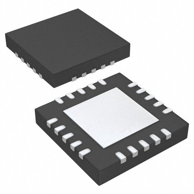
| 供应商器件封装 | 20-QFN(4x4) |
| 其它名称 | 296-36817-1 |
| 内部驱动器 | 是 |
| 包装 | 剪切带 (CT) |
| 安装类型 | 表面贴装 |
| 封装/外壳 | 20-WFQFN 裸露焊盘 |
| 工作温度 | -40°C ~ 85°C |
| 恒压 | - |
| 恒流 | - |
| 拓扑 | PWM,升压(升压) |
| 标准包装 | 1 |
| 电压-电源 | 4.5 V ~ 24 V |
| 电压-输出 | 4.5 V ~ 38 V |
| 类型-初级 | 背光 |
| 类型-次级 | 白色 LED |
| 输出数 | 6 |
| 频率 | 800kHz ~ 1.2MHz |


- 商务部:美国ITC正式对集成电路等产品启动337调查
- 曝三星4nm工艺存在良率问题 高通将骁龙8 Gen1或转产台积电
- 太阳诱电将投资9.5亿元在常州建新厂生产MLCC 预计2023年完工
- 英特尔发布欧洲新工厂建设计划 深化IDM 2.0 战略
- 台积电先进制程称霸业界 有大客户加持明年业绩稳了
- 达到5530亿美元!SIA预计今年全球半导体销售额将创下新高
- 英特尔拟将自动驾驶子公司Mobileye上市 估值或超500亿美元
- 三星加码芯片和SET,合并消费电子和移动部门,撤换高东真等 CEO
- 三星电子宣布重大人事变动 还合并消费电子和移动部门
- 海关总署:前11个月进口集成电路产品价值2.52万亿元 增长14.8%


PDF Datasheet 数据手册内容提取
Product Order Technical Tools & Support & Folder Now Documents Software Community TPS61187 SLVSA85E–JUNE2010–REVISEDDECEMBER2016 TPS61187 White-LED Driver For Notebooks With PWM Interface and Automatic Phase Shift 1 Features 2 Applications • InputVoltage4.5Vto24V NotebookLCDDisplayBacklight 1 • MaximumOutputVoltage38V 3 Description • Integrated2-A,40-VMOSFET The TPS61187 device provides a highly integrated • ProgrammableSwitchingFrequency300kHzto white-light-emitting-diode (WLED) driver solution for 1MHz notebook LCD backlight. This device has a built-in • AdaptiveBoostOutputtoWLEDVoltages high efficiency boost regulator with integrated 2-A, 40-V power MOSFET. The six current sink regulators • WidePWMDimmingFrequencyRange provide high precision current regulation and – 100Hzto50KHzforDirectPWMMode matching. In total, the device can support up to 60 – 100Hzto22KHzforFrequency WLEDs. In addition, the boost output automatically ProgrammableMode adjusts its voltage to the WLED forward voltage to optimizeefficiency. • 100:1DimmingRatioat20kHz • 10000:1DimmingRatioat200Hz(DirectPWM The TPS61187 supports the automatic phase-shift- mode) dimming method and direct-PWM-dimming method. During phase-shift-PWM dimming, the WLED current • SmallExternalComponents is turned on and turned off at the duty cycle • IntegratedLoopCompensation controlled by the input PWM signal, and each • SixCurrentSinksof30mAMaximum channel is shifted according to the frequency determined by an integrated pulse-width-modulation • 1.5%(Typical)CurrentMatching (PWM) signal. The frequency of this signal is resistor • PWMBrightnessInterfaceControl programmable, while the duty cycle is controlled • PWMPhaseShiftModeBrightnessDimming directly from an external PWM signal input to the MethodorDirectPWMDimmingMethod PWM pin. During direct PWM dimming, the WLED current is turned on and/or turned off synchronized • HBMESDProtection4kV withtheinputPWMsignal. • ProgrammableOvervoltageThreshold • Built-inWLEDOpen/ShortProtection DeviceInformation(1) • ThermalShutdown PARTNUMBER PACKAGE BODYSIZE(NOM) TS61183 WQFN(20) 4.00mm×4.00mm (1) For all available packages, see the orderable addendum at theendofthedatasheet. TypicalApplication –PhaseShiftPWMMode L1 4.5V~24V 10uH D1 C3 C1 4.7uF R4 2.2uF Open R5 VIN FAULT SW VDDIO PGND C2 1.0uF R7 1.2KW OVC EN FSLCT R3 TPS61187 R8 499KW 10KW PWM IFB1 19.8mA VDD_GPIO IFB2 62RK1W ISET IIIIFFFFBBBB5634 Open FPO AGND R/MFPOWDEM R2 9.09KW 1 An IMPORTANT NOTICE at the end of this data sheet addresses availability, warranty, changes, use in safety-critical applications, intellectualpropertymattersandotherimportantdisclaimers.PRODUCTIONDATA.
TPS61187 SLVSA85E–JUNE2010–REVISEDDECEMBER2016 www.ti.com Table of Contents 1 Features.................................................................. 1 7.4 DeviceFunctionalModes........................................12 2 Applications........................................................... 1 8 ApplicationandImplementation........................ 17 3 Description............................................................. 1 8.1 ApplicationInformation............................................17 4 RevisionHistory..................................................... 2 8.2 TypicalApplication .................................................17 5 PinConfigurationandFunctions......................... 3 9 PowerSupplyRecommendations...................... 20 6 Specifications......................................................... 4 10 Layout................................................................... 21 6.1 AbsoluteMaximumRatings......................................4 10.1 LayoutGuidelines.................................................21 6.2 ESDRatings..............................................................4 10.2 LayoutExample....................................................21 6.3 RecommendedOperatingConditions.......................4 11 DeviceandDocumentationSupport................. 22 6.4 ThermalInformation..................................................5 11.1 DeviceSupport......................................................22 6.5 ElectricalCharacteristics...........................................5 11.2 ReceivingNotificationofDocumentationUpdates22 6.6 TypicalCharacteristics..............................................7 11.3 CommunityResources..........................................22 7 DetailedDescription............................................ 10 11.4 Trademarks...........................................................22 7.1 Overview.................................................................10 11.5 ElectrostaticDischargeCaution............................22 7.2 FunctionalBlockDiagram.......................................10 11.6 Glossary................................................................22 7.3 FeatureDescription.................................................11 12 Mechanical,Packaging,andOrderable Information........................................................... 22 4 Revision History NOTE:Pagenumbersforpreviousrevisionsmaydifferfrompagenumbersinthecurrentversion. ChangesfromRevisionD(February2012)toRevisionE Page • AddedDeviceInformationandPinConfigurationandFunctionssections,ESDRatingsandThermalInformation tables,FeatureDescription,DeviceFunctionalModes,ApplicationandImplementation,PowerSupply Recommendations,Layout,DeviceandDocumentationSupport,andMechanical,Packaging,andOrderable Informationsections................................................................................................................................................................ 1 • DeletedOrderingtable-informationinPOA ......................................................................................................................... 1 • Addedlast2sentencesofIFBPinUnused......................................................................................................................... 12 ChangesfromRevisionC(September2011)toRevisionD Page • ChangedFigure18XaxisunitfrommAtoA....................................................................................................................... 20 • ChangedFigure19XaxisunitfrommAtoA....................................................................................................................... 20 ChangesfromRevisionB(April2011)toRevisionC Page • AddedadescriptionparagraphandreplacedFigure15inthePHASESHIFTPWMDIMMINGsection............................ 13 ChangesfromRevisionA(July2010)toRevisionB Page • ChangedinABSMAXtable,inrow"Allotherpins",MAXcol:from3.6to3.7...................................................................... 4 ChangesfromOriginal(June2010)toRevisionA Page • ChangedTypicalApplicationgraphic..................................................................................................................................... 1 • Changedceramiccapacitorvalue,attachedtoVDDIO,from0.1to1µF.............................................................................. 3 • ChangedbypasscapacitorvalueinSUPPLYVOLTAGEsectionfrom0.1to1µF............................................................. 11 • ChangedBRIGHTNESSDIMMINGCONTROLsection....................................................................................................... 12 • DeletedPWMBRIGHTNESSCONTROLINTERFACEsection.......................................................................................... 13 2 SubmitDocumentationFeedback Copyright©2010–2016,TexasInstrumentsIncorporated ProductFolderLinks:TPS61187
TPS61187 www.ti.com SLVSA85E–JUNE2010–REVISEDDECEMBER2016 5 Pin Configuration and Functions RTJPackage 20-PinQFNWithThermalPad TopView T M L PW VIN FAU NC SW 20 19 18 17 16 VDDIO 1 15 PGND EN 2 14 OVC TPS61187 RFPWM FSLCT 3 13 /MODE ISET 4 12 IFB1 FPO 5 11 IFB2 6 7 8 9 10 6 5 4 D 3 B B B N B F F F G F I I I I PinFunctions PIN TYPE DESCRIPTION NO. NAME 1 VDDIO A Internalpre-regulator.Connecta1-µFceramiccapacitortoVDDIO. 2 EN I Enable Switchingfrequencyselectionpin.Usearesistortosetthefrequencybetween300kHz 3 FSLCT I to1MHz. Full-scaleLEDcurrentsetpin.Connectingaresistortothepinprogramsthecurrent 4 ISET I level. 5 FPO O FaultprotectionoutputtoindicatefaultconditionsincludingOVP,OC,andOT. 6,7,8, IFB1toIFB6 A Regulatedcurrentsinkinputpins 10,11,12 9, GND G Analogground 13 RFPWM/MODE I Dimmingfrequencyprogrampinwithanexternalresistor/modeselection,see(1) 14 OVC A Overvoltageclamppin/voltagefeedback,see(1) 15 PGND G Powerground 16 SW A DrainconnectionoftheinternalpowerFET 17 NC — Noconnection 18 FAULT O FaultpintodriveexternalISOFET 19 VIN A Supplyinputpin 20 PWM I PWMsignalinputpin — ThermalPad — ConnecttoGNDplaneforbetterthermalperformance. A:Analog;G:Ground;I:Input:O:Output;P:Power (1) SeeApplicationandImplementationfordetails. Copyright©2010–2016,TexasInstrumentsIncorporated SubmitDocumentationFeedback 3 ProductFolderLinks:TPS61187
TPS61187 SLVSA85E–JUNE2010–REVISEDDECEMBER2016 www.ti.com 6 Specifications 6.1 Absolute Maximum Ratings overoperatingfree-airtemperaturerange(unlessotherwisenoted) (1) MIN MAX UNIT VIN,FAULT –0.3 24 V FPO –0.3 7 V SW –0.3 40 V Voltagerange(2) EN,PWM,IFB1toIFB4 –0.3 20 V VDDIO –0.3 3.7 V Allotherpins –0.3 3.6 V Continuouspowerdissipation SeeThermalInformation Operatingjunctiontemperaturerange –40 150 °C Storagetemperaturerange,T –65 150 °C stg (1) Stressesbeyondthoselistedunderabsolutemaximumratingsmaycausepermanentdamagetothedevice.Thesearestressratings only,andfunctionaloperationofthedeviceattheseoranyotherconditionsbeyondthoseindicatedunderRecommendedOperating Conditionsisnotimplied.Exposuretoabsolute-maximum-ratedconditionsforextendedperiodsmayaffectdevicereliability. (2) Allvoltagevaluesarewithrespecttonetworkgroundterminal. 6.2 ESD Ratings VALUE UNIT Human-bodymodel(HBM),perANSI/ESDA/JEDECJS-001(1) ±4000 V Electrostaticdischarge Charged-devicemodel(CDM),perJEDECspecificationJESD22-C101(2) ±1500 V (ESD) Machinemodel 200 (1) JEDECdocumentJEP155statesthat500-VHBMallowssafemanufacturingwithastandardESDcontrolprocess. (2) JEDECdocumentJEP157statesthat250-VCDMallowssafemanufacturingwithastandardESDcontrolprocess. 6.3 Recommended Operating Conditions overoperatingfree-airtemperaturerange(unlessotherwisenoted) MIN NOM MAX UNIT V Inputvoltage 4.5 24 V IN V Outputvoltage V 38 V OUT IN L1 Inductor,600-kHzto1-MHzswitchingfrequency 10 22 µH L1 Inductor,300-kHzto600-kHzswitchingfrequency 22 47 µH C Inputcapacitor 1 µF I C Outputcapacitor 1 4.7 10 µF O F IFBxPWMdimmingfrequency-frequencyprogrammablemode 0.1 22(1) KHz PWM_O F IFBxPWMdimmingfrequency-directPWMmode 0.1 50 KHz PWM_O F PWMinputsignalfrequency 0.1 22 KHz PWM_I F Boostregulatorswitchingfrequency 300 1000 KHz BOOST T Operatingfree-airtemperature –40 85 °C A T Operatingjunctiontemperature –40 125 °C J (1) 5-µsminimumpulseontime. 4 SubmitDocumentationFeedback Copyright©2010–2016,TexasInstrumentsIncorporated ProductFolderLinks:TPS61187
TPS61187 www.ti.com SLVSA85E–JUNE2010–REVISEDDECEMBER2016 6.4 Thermal Information TPS61187 THERMALMETRIC(1) RTJ(WQFN) UNIT 20PINS R Junction-to-ambientthermalresistance 39.9 °C/W θJA R Junction-to-case(top)thermalresistance 34.0 °C/W θJC(top) R Junction-to-boardthermalresistance 9.9 °C/W θJB ψ Junction-to-topcharacterizationparameter 0.6 °C/W JT ψ Junction-to-boardcharacterizationparameter 9.5 °C/W JB R Junction-to-case(bottom)thermalresistance 2 °C/W θJC(bottom) (1) Formoreinformationabouttraditionalandnewthermalmetrics,seeSemiconductorandICPackageThermalMetrics. 6.5 Electrical Characteristics V =12V,PWM/EN=high,IFBcurrent=20mA,IFBvoltage=500mV,T =–40°Cto+85°C,typicalvaluesareatT = IN A A 25°C(unlessotherwisenoted) PARAMETER TESTCONDITIONS MIN TYP MAX UNIT SUPPLYCURRENT V Inputvoltagerange 4.5 24 V IN Deviceenable,switching1MHzand I OperatingquiescentcurrentintoV noload, 4 mA Q_VIN IN V =24V IN VDDIO VDDIOpinoutputvoltage I =5mA 3 3.3 3.6 V LOAD V =12V,EN=low 11 IN I Shutdowncurrent µA SD V =24V,EN=low 16 IN V rampdown 3.5 IN V V undervoltagelockoutthreshold V IN_UVLO IN V rampup 3.75 IN V V undervoltagelockouthysterisis 250 mV IN_Hys IN PWM V ENlogichighthreshold EN 2.1 H V ENlogiclowthreshold EN 0.8 L V V PWMlogichighthreshold PWM 2.1 H V PWMlogiclowthreshold PWM 0.8 L R PulldownresistoronPWMandEN 400 800 1600 kΩ PD CURRENTREGULATION V ISETpinvoltage 1.204 1.229 1.253 V ISET K Currentmultiplier 980 ISET I =20µA,0°Cto70°C –2% 2% ISET I Currentaccuracy FB I =20µA,–40°Cto85°C –2.3% 2.3% ISET K (I –I )/I I =20µA 1.3% m max min AVG ISET IFBvoltage=15V,eachpin 2 5 I IFBpinleakagecurrent µA leak IFBvoltage=5V,eachpin 1 2 I Currentsinkmaxoutputcurrent IFB=350mV 30 mA IFB_max f PWMdimmingfrequency R =9.09kΩ 20 kHz dim FPWM Copyright©2010–2016,TexasInstrumentsIncorporated SubmitDocumentationFeedback 5 ProductFolderLinks:TPS61187
TPS61187 SLVSA85E–JUNE2010–REVISEDDECEMBER2016 www.ti.com Electrical Characteristics (continued) V =12V,PWM/EN=high,IFBcurrent=20mA,IFBvoltage=500mV,T =–40°Cto+85°C,typicalvaluesareatT = IN A A 25°C(unlessotherwisenoted) PARAMETER TESTCONDITIONS MIN TYP MAX UNIT BOOSTOUTPUTREGULATION V Outputvoltageupthreshold MeasuredonV 350 mV IFB_L IFB(min) V Ouputvoltagedownthreshold MeasuredonV 650 mV IFB_H IFB(min) POWERSWITCH R PWMFETon-resistance V =12V 0.25 0.35 Ω PWM_SW IN I PWMFETleakagecurrent V =40V,T =25°C 2 µA LN_NFET SW A OSCILLATOR f Oscillatorfrequency R =499kΩ 0.8 1 1.2 MHz S FSW D Maximumdutycycle IFB=0 94% max OC,SC,OVP,ANDSS I N-channelMOSFETcurrentlimit D=D 2 3 A LIM max Ouputvoltageclampprogram V 1.90 1.95 2 V CLAMP_TH threshold V IFBovervoltagethreshold MeasuredontheIFBxpin,IFBon 12 13.5 15 V OVP_IFB FPO,FAULT V FPOLogiclowvoltage I =0.5mA 0.4 V FPO_L _SOURCE V Faulthighvoltage MeasuredasV –V 0.1 V FAULT_HIGH IN FAULT MeasuredasV –V ,Sink,10 V Faultlowvoltage IN FAULT 6 8 10 V FAULT_LOW µA I Maximumsinkcurrent V –V =0V 20 µA FAULT IN FAULT THERMALSHUTDOWN Thermalshutdownthreshold 150 T °C shutdown Thermalshutdownhysteresis 15 6 SubmitDocumentationFeedback Copyright©2010–2016,TexasInstrumentsIncorporated ProductFolderLinks:TPS61187
TPS61187 www.ti.com SLVSA85E–JUNE2010–REVISEDDECEMBER2016 6.6 Typical Characteristics 6.6.1 TableOfGraphs TITLE DESCRIPTION FIGURE Dimminglinearity V =32V,V =8V,12V,24V,F =20KHz,L=10µH,R =62kΩ Figure1 OUT IN DIM ISET Dimminglinearity V =32V,V =8V,12V,24V,F =200Hz,L=10µH,R =62kΩ Figure2 OUT IN DIM ISET Boostswitchingfrequency V =12V,V =33.8V,L=10µH,R =62kΩ Figure3 IN OUT ISET Phaseshiftdimmingfrequency V =12V,V =33.8V,L=10µH,R =62kΩ Figure4 IN OUT ISET Switchwaveform V =8V,V =33.8V,F =20kHz,Duty=100%,L=10µH,R =62kΩ Figure5 IN OUT DIM ISET V =12V,V =33.8V,F =20kHz,Duty=100%,L=10µH,R =62 Switchwaveform IN OUT DIM ISET Figure6 kΩ PhaseshiftPWMdimmingF =200Hz, DIM V =12V,V =33.8V,F =20kHz,Duty=45%,L=10µH,R =62kΩ Figure7 duty=50% IN OUT DIM ISET PhaseshiftPWMdimmingF =20KHz, DIM V =12V,V =33.8V,F =20kHz,Duty=51%,L=10µH,R =62kΩ Figure8 duty=50% IN OUT DIM ISET OutputrippleofPhaseshiftPWM V =12V,V =33.8V,F =20kHz,Duty=50%,L=10µH,R =62kΩ Figure9 dimming IN OUT DIM ISET OutputrippleofPhaseshiftPWM V =12V,V =33.8V,F =20kHz,Duty=70%,L=10µH,R =62kΩ Figure10 dimming IN OUT DIM ISET V =12V,V =33.8V,F =20kHz,Duty=100%,L=10µH,R =62 Start-upwaveform IN OUT DIM ISET Figure11 kΩ Start-upwaveform V =12V,V =33.8V,F =20kHz,Duty=50%,L=10µH,R =62kΩ Figure12 IN OUT DIM ISET 0.12 0.12 FDIM= 20 KHz FDIM= 200 Hz 0.1 VI= 8 V 0.1 VI= 8 V urrent -A 0.08 VI= 24 V VI= 12 V urrent -A 0.08 VI= 24 V VI= 12 V C 0.06 C 0.06 ut ut p p ut ut - O 0.04 - O 0.04 O O I I 0.02 0.02 0 0 0 10 20 30 40 50 60 70 80 90 100 0 10 20 30 40 50 60 70 80 90 100 Dimming duty cycle - % Dimming duty cycle - % Figure1.OutputCurrent Figure2.OutputCurrent Copyright©2010–2016,TexasInstrumentsIncorporated SubmitDocumentationFeedback 7 ProductFolderLinks:TPS61187
TPS61187 SLVSA85E–JUNE2010–REVISEDDECEMBER2016 www.ti.com 1100 20000 VI= 8 V VI= 8 V 1000 Hz 15000 Switching Frequency - 789000000 mming Frequency - Hz10000 - Di 5000 fs 600 500 0 500 600 700 800 900 1000 10 110 210 310 410 510 610 710 810 910 RFSLCT - kW RFPWM - kW Figure3.SwitchingFrequency Figure4.DimmingFrequency VO VO 100 mV/div 100 mV/div AC AC SW SW 20 V/div 20 V/div DC DC Inductor Inductor Current Current 500 mA/div 500 mA/div DC DC Figure5.SwitchWaveform Figure6.SwitchWaveform IFB1 IFB1 10 V/div 10 V/div DC DC IFB2 IFB2 10 V/div 10 V/div DC DC IFB3 IFB3 10 V/div 10 V/div DC DC Output Output Current Current 50 mA/div 50 mA/div DC DC Figure7.Phase-ShiftWaveform Figure8.Phase-ShiftWaveform 8 SubmitDocumentationFeedback Copyright©2010–2016,TexasInstrumentsIncorporated ProductFolderLinks:TPS61187
TPS61187 www.ti.com SLVSA85E–JUNE2010–REVISEDDECEMBER2016 IFB1 IFB1 10 V/div 10 V/div DC DC IFB2 IFB2 10 V/div 10 V/div DC DC VO VO 100 mV/div 100 mV/div AC AC Output Output Current Current 50 mA/div 50 mA/div DC DC Figure9.OutputRippleWaveform Figure10.OutputRippleWaveform EN EN 5 V/div 5 V/div DC DC VDDIO VDDIO 5 V/div 5 V/div DC DC VO VO 10 mV/div 10 mV/div DC DC Output Output Current Current 50 mA/div 50 mA/div DC DC Figure11.Start-UpWaveform Figure12.Start-UpWaveform Copyright©2010–2016,TexasInstrumentsIncorporated SubmitDocumentationFeedback 9 ProductFolderLinks:TPS61187
TPS61187 SLVSA85E–JUNE2010–REVISEDDECEMBER2016 www.ti.com 7 Detailed Description 7.1 Overview The TPS61187 is a high-efficiency, high-output-voltage WLED driver for notebook panel backlighting applications. The advantages of WLEDs compared to cold cathode fluorescent lamp (CCFL) backlights are higher power efficiency and lower profile design. Due to the large number of WLEDs required to provide backlighting for medium to large display panels, the LEDs must be arranged in parallel strings of several LEDs in series. Therefore, the backlight driver for battery powered systems is almost always a boost regulator with multiple current sink regulators. Having more WLEDs in series reduces the number of parallel strings, and therefore improves overall current matching. However, the efficiency of the boost regulator declines due to the needforhighoutputvoltage.Also,theremustbeenoughwhiteLEDsinseriestoensuretheoutputvoltagestays abovetheinputvoltagerange. The TPS61187 device has integrated all of the key function blocks to power and control up to 60 WLEDs. The device includes a 40-V, 2-A boost regulator, six 30-mA current sink regulators, and a protection circuit for overcurrent,overvoltage,openLED,shortLED,andoutputshort-circuitfailures. The TPS61187 device integrates auto phase shifted PWM dimming methods with the PWM interface to reduce the output ripple voltage and audible noise. An optional direct PWM mode is user selectable through the MODE selectionfunction. 7.2 Functional Block Diagram Optional L Diode VIN OUTPUT C1 R6 C4 2.2uF C3 4.7uF R4 FAULT18 NC17 SW 16 VIN 19 Fault Fault OVP Linear Protection Condition Protection VDDIO Regulator OVC 1 14 C2 OVC R5 0.1uF R Q VDD_GPIO S Vref PGND 15 R7 Slope S RFPO 5 Compensation IFB1 IFB2 Optional Comp Error A D MUX Detector IIIFFFBBB345 Amp 3 Oscillator Vref IFB6 R3 12 IFB1 FSLCT PWM Signal Generator / MODE EA selection 4 Current Mirror LMEDax cimururemnt DCimonmtrionlg EN R2 13 SeLloegcticion PGWeMne Sraigtonral Current Sink 9 AGND R1 RFPWM Phase RISETH /MODE Shift Current Sink 11 IFB2 PWM Current Sink 10 IFB3 / Direct PWM Direct Current Sink 8 IFB4 PWM 20 Frequency/ Duty PWM Current Sink 7 IFB5 duty decoding control Current Sink 6 IFB6 circuit Signal oscillator OCP TSD Open/Short EN 2 Shutdown IFB no use Protection Protection LED 10 SubmitDocumentationFeedback Copyright©2010–2016,TexasInstrumentsIncorporated ProductFolderLinks:TPS61187
TPS61187 www.ti.com SLVSA85E–JUNE2010–REVISEDDECEMBER2016 7.3 Feature Description 7.3.1 SupplyVoltage TheTPS61187devicehasabuilt-inlinearregulatortosupplythedeviceanalogandlogiccircuit.TheVDDIOpin, outputoftheregulator,isconnectedtoa1-µFbypasscapacitorfortheregulatortobecontrolledinastableloop. VDDIO does not have high current sourcing capability for external use but it can be tied to the EN pin for start up. 7.3.2 BoostRegulatorandProgrammableSwitchFrequency(FSCLT) The fixed-frequency PWM boost converter uses current-mode control and has integrated loop compensation. The internal compensation ensures stable output over the full input and output voltage ranges assuming the recommended inductance and output capacitance values shown in Typical Application– Phase Shift PWM Mode are used. The output voltage of the boost regulator is automatically set by the device to minimize voltage drop acrosstheIFBpins.ThedeviceregulatesthelowestIFBpinto350mVandconsistentlyadjuststheboostoutput voltage to account for any changes in LED forward voltages. If the input voltage is higher than the sum of the WLED forward voltage drops (for example, at low duty cycles), the boost converter is not able to regulate the output due to its minimum duty cycle limitation. In this case, increase the number of WLEDs in series or include series ballast resistors in order to provide enough headroom for the converter to boost the output voltage. Because the TPS61187 integrates a 2-A, 40-V power MOSFET, the boost converter can provide up to a 38-V outputvoltage. The TPS61187 switching frequency can be programmed between 300 kHz to 1 MHz by the resistor value on the FSLCTpinaccordingtoEquation1: 5 ´ 1011 F = SW R FSLCT where • R =FSCLTpinresistor (1) FSLCT SeeFigure3forboostconverterswitchingfrequencyadjustmentresistorR selection. FSLCT The adjustable switching frequency feature provides the user with the flexibility of choosing a faster switching frequency, as well as an inductor with smaller inductance and footprint or slower switching frequency, and therefore, potentially higher efficiency due to lower switching losses. Use Equation 1 or refer to Table 1 to select thecorrectvalue: Table1.R Recommendations FSLCT R F FLCT SW 833kΩ 600KHz 625kΩ 800KHz 499kΩ 1MHz 7.3.3 LEDCurrentSinks The six current sink regulators embedded in the TPS61187 can be collectively configured to provide up to a maximum of 30 mA each. These six specialized current sinks are accurate to within ±2% maximum for currents at20mA,withastring-to-stringdifferenceof ±1.5%typical. The IFB current must be programmed to the highest WLED current expected using the ISETH pin resistor and Equation2. V I = ISETH ´ K FB ISET R ISETH where • K =980(currentmultiple) ISET • V =1.229V(ISETHpinvoltage) ISETH • R =ISETHpinresistor (2) ISETH Copyright©2010–2016,TexasInstrumentsIncorporated SubmitDocumentationFeedback 11 ProductFolderLinks:TPS61187
TPS61187 SLVSA85E–JUNE2010–REVISEDDECEMBER2016 www.ti.com 7.3.4 EnableandStart-up The internal regulator which provides VDDIO wakes up as soon as V is applied even when EN is low. This IN allows the device to start when EN is tied to the VDDIO pin. VDDIO does not come to full regulation until EN is high. The TPS61187 checks the status of all current feedback channels and shuts down any unused feedback channels.Itisrecommendedtoshorttheunusedchannelstogroundforfasterstart-up. After the device is enabled, if the PWM pin is left floating, the output voltage of the TPS61187 regulates to the minimum output voltage. Once the device detects a voltage on the PWM pin, the TPS61187 begins to regulate the IFB pin current, as pre-set per the ISETH pin resistor, according to the duty cycle of the signal on the PWM pin. The boost converter output voltage rises to the appropriate level to accommodate the sum of the white LED stringwiththehighestforwardvoltagedropsplustheheadroomofthecurrentsinkatthatcurrent. Pulling the EN pin low shuts down the device, resulting in the device consuming less than 11 µA in shutdown mode. 7.3.5 IFBPinUnused The TPS61187 has open/short string detection. For an unused IFB string, simply short it to ground or leave it open. TI recommend shorting unused IFB pins to ground for faster start-up. After EN is pulled high, the TPS61187 outputs about 40–µA current to each current channel for 4 ms and measures the voltage on each channel.Ifthevoltageonanychannelislessthan600mV,thechannelisturnedoffandremovedfromtheboost controlloopasunusedchannel. 7.4 Device Functional Modes 7.4.1 BrightnessDimmingControl TheTPS61187hasauto-phase-shiftedPWMdimmingcontrolwiththePWMcontrolinterface. The internal decoder block detects duty information from the input PWM signal, saves it in an eight bit register and delivers it to the output PWM dimming control circuit. The output PWM dimming control circuit turns on/off sixoutputcurrentsinksatthePWMfrequencysetbyRFPWMandthedutycyclefromthedecoderblock. The TPS61187 also has direct PWM dimming control with the PWM control interface. In direct PWM mode, each current sink turns on/off at the same frequency and duty cycle as the input PWM signal. See the Mode Selection–Phase-ShiftPWMOrDirectPWMDimming fordimmingmodeselection. Wheninphase-shiftedPWMmode,TIrecommendsinsertionofaseriesresistorof10kΩto20kΩvaluecloseto the PWMIN pin. This resistor together with an internal capacitor forms a low pass R-C filter with 30-ns to 60-ns time constant. This prevents possible high frequency noises being coupled into the input PWM signal and causinginterferencetotheinternaldutycycledecodingcircuit.However,itisnotnecessaryfordirectPWMmode becausethedutycycledecodingcircuitisdisabledduringthedirectPWMmode. 7.4.2 AdjustablePWMDimmingFrequencyandModeSelection(R_FPWM/MODE) The TPS61187 can operate in auto phase shift mode or direct PWM mode. Tying the RFPWM/MODE pin to VDDIO forces the device to operate in direct PWM mode. A resistor between the RFPWM/MODE pin and ground setsthedeviceintoauto-phase-shiftmodeandthevalueoftheresistordeterminesthePWMdimmingfrequency. UseEquation3orrefertoTable2toselectthecorrectvalue: 1.818 ´ 108 F = DIM R FPWM where • R =RFPWMpinresistor (3) FPWM 12 SubmitDocumentationFeedback Copyright©2010–2016,TexasInstrumentsIncorporated ProductFolderLinks:TPS61187
TPS61187 www.ti.com SLVSA85E–JUNE2010–REVISEDDECEMBER2016 Table2.R Recommendations FPWM R F FPWM DIM 866kΩ 210Hz 432kΩ 420Hz 174kΩ 1.05kHz 9.09kΩ 20kHz 7.4.3 ModeSelection– Phase-ShiftPWMOrDirectPWMDimming The phase-shift PWM dimming method or direct PWM dimming method can be selected through the RFPWM pin. By attaching an external resistor to the RFPWM pin, the default phase shift PWM mode can be selected. To select direct PWM mode, the RFPWM pin needs to be tied to the VDDIO pin. The RFPWM/MODE pin can be noise sensitive when R2 has high impedance. In this case, careful layout or a parallel bypassing capacitor improvesnoisesensitivitybutthevalueoftheparallelcapacitormaynotexceed33pFforoscillatorstability. RFPWM VDDIO /MODE Pin13 RFPWM /MODE R2 9.09KW Pin13 Figure14.DirectPWM-Dimming-ModeSelection Figure13.Phase-ShiftPWM-Dimming-ModeSelection 7.4.3.1 Phase-ShiftPWMDimming In phase-shift PWM mode, all current feedback channels are turned on and off at F frequency with a constant DIM delay. However, the number of used channels and PWM dimming frequency determine the delay time between twoneighboringchannelsperEquation4. 1 T_delay= n ´ F DIM where • nisthenumberofusedchannels • F isthePWMdimmingfrequencythatisdeterminedbythevalueofR ontheRFPWMpin (4) DIM FPWM Figure15providesthedetailedtimingdiagramofthephase-shiftPWMdimmingmode. In phase-shift PWM mode, the internal decoder converts the duty-cycle information from the applied PWM signal at the PWM pin into an 8-bit digital signal and stores it into a register. The integrated dimming control circuit reconstructs the PWM duty cycle per the register value and sends it to each of the current sinks. In order to avoid any flickering while the duty cycle information is reconstructed from the register, one LSB (1/256) of duty cycle hysteresis is included which results in 1/256 resolution when incrementing the applied signal's duty cycle but2/256resolutionwhendecrementingthedutycycle. Copyright©2010–2016,TexasInstrumentsIncorporated SubmitDocumentationFeedback 13 ProductFolderLinks:TPS61187
TPS61187 SLVSA85E–JUNE2010–REVISEDDECEMBER2016 www.ti.com PWM 25% 50ms IFB1 IFB2 IFB3 IFB4 IFB5 IFB6 - PWM input 25%, Iset = 20 mA 8.33ms - PWM output 20 kHz, T = 50ms n = 6, T/n = 8.33ms Figure15. Phase-ShiftPWMDimmingTimingDiagram 7.4.3.2 DirectPWMDimming In direct PWM mode, all current feedback channels are turned on and off and are synchronized with the input PWMsignal. 14 SubmitDocumentationFeedback Copyright©2010–2016,TexasInstrumentsIncorporated ProductFolderLinks:TPS61187
TPS61187 www.ti.com SLVSA85E–JUNE2010–REVISEDDECEMBER2016 PWM IFB_CH1 IFB_CH2 IFB_CH3 IFB_CH4 IFB_CH5 IFB_CH6 Input PWM frequency and6-CH output dimming frequencyare exactly same. Figure16. DirectPWMDimmingTimingDiagram 7.4.4 OvervoltageClampandVoltageFeedback(OVC/FB) The correct divider ratio is important for optimum operation of the TPS61187. Use the following guidelines to choose the divider value. It can be noise sensitive if R and R have high impedance. Careful layout is upper down required.Also,chooselowerresistancevaluesforR andR whenpowerdissipationallows. upper down 1. Determinethemaximumoutputvoltage,V ,forthesystemaccordingtothenumberofseriesWLEDs. O 2. Select an R resistor value (1 MΩ for a typical application; a lower value such as 100 kΩ for a noisy upper environment). 3. CalculateR usingEquation5 down æR ö V = ç upper +1÷ ´ V OVP OV_TH èRdown ø where • V =1.95V (5) OV_TH When the device detects that the OVC pin exceeds 1.95 V typical, indicating that the output voltage is over the setthresholdpoint,theOVCcircuitryclampstheoutputvoltagetothesetthreshold. Copyright©2010–2016,TexasInstrumentsIncorporated SubmitDocumentationFeedback 15 ProductFolderLinks:TPS61187
TPS61187 SLVSA85E–JUNE2010–REVISEDDECEMBER2016 www.ti.com 7.4.5 Current-SinkOpenProtection For the TPS61187, if one of the WLED strings is open, the device automatically detects and disables that string. The device detects the open WLED string by sensing no current in the corresponding IFB pin. As a result, the device deactivates the open IFB pin and removes it from the voltage feedback loop. Subsequently, the output voltage drops and is regulated to the minimum voltage required for the connected WLED strings. The IFB current oftheconnectedWLEDstringsremainsinregulation. If any IFB pin voltage exceeds the IFB overvoltage threshold (13.5 V typical), the device turns off the corresponding current sink and removes this IFB pin from the regulation loop. The current regulation of the remaining IFB pins is not affected. This condition often occurs when there are several shorted WLEDs in one string.WLEDmismatchtypicallydoesnotcreatelargevoltagedifferencesamongWLEDstrings. The device only shuts down if it detects that all of the WLED strings are open. If an open string is reconnected again,apower-onreset(POR)orENpintogglingisrequiredtoreactivateapreviouslydeactivatedstring. 7.4.6 OvercurrentandShort-CircuitProtection The TPS61187 has a pulse-by-pulse over-current limit of 2 A (minimum). The PWM switch turns off when the inductor current reaches this current threshold. The PWM switch remains off until the beginning of the next switching cycle. This protects the device and external components during on overload conditions. When there is a sustained overcurrent condition, the device turns off and requires a POR or EN pin toggling to restart. Under severe overload and/or short-circuit conditions, the boost output voltage can be pulled below the required regulated voltage to keep all of the white LEDs operating. Under thses conditions, the current flows directly from input to output through the inductor and schottky diode. To protect the TPS61187, the device shuts down immediately.ThedevicerestartsafterinputPORorENpintoggling. 7.4.7 ThermalProtection When the junction temperature of the TPS61187 is over 150°C, the thermal protection circuit is triggered and shutsdownthedeviceimmediately.OnlyaPORorENpintogglingclearstheprotectionandrestartsthedevice. 16 SubmitDocumentationFeedback Copyright©2010–2016,TexasInstrumentsIncorporated ProductFolderLinks:TPS61187
TPS61187 www.ti.com SLVSA85E–JUNE2010–REVISEDDECEMBER2016 8 Application and Implementation NOTE Information in the following applications sections is not part of the TI component specification, and TI does not warrant its accuracy or completeness. TI’s customers are responsible for determining suitability of components for their purposes. Customers should validateandtesttheirdesignimplementationtoconfirmsystemfunctionality. 8.1 Application Information The TPS61187 provides a high-performance LED lighting solution for tablets, notebooks, monitors, and a variety of industrial designs. The device can drive 6 strings of 10 series LEDs in a compact and highly efficient solution. The TPS61187 provides a gate driver to an external P-channel MOSFET, which can be turned off during device shutdownorfaultcondition. 8.2 Typical Application L1 4.5V~24V 10uH D1 C3 C1 4.7uF R4 2.2uF Open R5 VIN FAULT SW VDDIO PGND C2 1.0uF R7 1.2KW OVC EN FSLCT R3 TPS61187 499KW R8 10KW PWM 19.8mA IFB1 VDD_GPIO IFB2 IFB3 ISET IFB4 R1 62KW IFB5 IFB6 Open FPO RFPWM AGND /MODE R2 9.09KW Figure17. TPS61187TypicalApplication Copyright©2010–2016,TexasInstrumentsIncorporated SubmitDocumentationFeedback 17 ProductFolderLinks:TPS61187
TPS61187 SLVSA85E–JUNE2010–REVISEDDECEMBER2016 www.ti.com Typical Application (continued) 8.2.1 DesignRequirements FortypicalWLED-driverapplications,usetheparameterslistedinTable3. Table3.DesignParameters DESIGNPARAMETER EXAMPLEVALUE Inputvoltage 4Vto24V Outputvoltage 38V(maximum) LEDstringcurrent 30mA(maximum) Switchingfrequency 280kHzto1MHz 8.2.2 DetailedDesignProcedure 8.2.2.1 InductorSelection Because selection of the inductor affects power supply steady state operation, transient behavior, and loop stability, the inductor is the most important component in switching power regulator design. There are three specifications most important to the performance of the inductor: inductor value, DC resistance (DCR), and saturation current. The TPS61187 is designed to work with inductor values between 10 µH and 47 µH. A 10-µH inductor is typically available in a smaller or lower profile package, while a 47-µH inductor may produce higher efficiency due to a slower switching frequency and/or lower inductor ripple. If the boost output current is limited by the over-current protection of the device, using a 10-µH inductor and the highest switching frequency maximizescontrolleroutputcurrentcapability. Internal loop compensation for PWM control is optimized for the external component values, including typical tolerances, recommended in Table 4. Inductor values can have ±20% tolerance with no current bias. When the inductor current approaches saturation level, its inductance can decrease 20% to 35% from the 0-A value depending on how the inductor vendor defines saturation. In a boost regulator, the inductor dc current can be calculatedwithEquation6. Vout ´ Iout I = DC Vin ´ h where • V =boostoutputvoltage OUT • IOUT=boostoutputcurrent • VIN=boostinputvoltage • η=powerconversionefficiency,use90%forTPS61187applications (6) Theinductorcurrentpeak-to-peakripplecanbecalculatedwithEquation7. 1 I = PP æ 1 1 ö L ´ ç + ÷ ´ FS èVout - Vin Vinø where • I =inductorpeak-to-peakripple PP • L=inductorvalue • F =Switchingfrequency S • V =boostoutputvoltage OUT • V =boostinputvoltage (7) IN Therefore,thepeakcurrentseenbytheinductoriscalculatedwithEquation8. I I =I + PP P DC 2 (8) Selectaninductorwithasaturationcurrentoverthecalculatedpeakcurrent.Tocalculatetheworst-caseinductor peakcurrent,usetheminimuminputvoltage,maximumoutputvoltage,andmaximumloadcurrent. 18 SubmitDocumentationFeedback Copyright©2010–2016,TexasInstrumentsIncorporated ProductFolderLinks:TPS61187
TPS61187 www.ti.com SLVSA85E–JUNE2010–REVISEDDECEMBER2016 Regulator efficiency is dependent on the resistance of its high current path and switching losses associated with the PWM switch and power diode. Although the TPS61187 device has optimized the internal switch resistances, the overall efficiency is affected by the inductor DCR. Lower DCR improves efficiency. However, there is a trade off between DCR and inductor footprint; furthermore, shielded inductors typically have higher DCR than unshieldedones.Table4liststherecommendedinductors. Table4.RecommendedInductorForTPS61187 L(µH) DCR(mΩ) I (A) SIZE(L×W×Hmm) SAT TOKO A915AY–4R7M 4.7 38 1.87 5.2×5.2×3.0 A915AY–100M 10 75 1.24 5.2×5.2×3.0 TDK SLF6028T–4R7N1R6 4.7 38 1.87 5.2×5.2×3.0 SLF6028T–4R7N1R6 10 75 1.24 5.2×5.2×3.0 8.2.2.2 OutputCapacitorSelection The output capacitor is mainly selected to meet the requirement for output ripple and loop stability. This ripple voltage is related to the capacitance of the capacitor and its equivalent series resistance (ESR). Assuming a capacitorwithzeroESR,theminimumcapacitanceneededforagivenripplecanbecalculatedwithEquation9: (Vout - Vin) ´ Iout Cout= Vout ´ F ´ Vripple S where • Vripple=peak-to-peakoutputripple (9) TheadditionalpartoftheripplecausedbyESRiscalculatedusing:Vripple_ESR=I ×RESR OUT Due to its low ESR, Vripple_ESR can be neglected for ceramic capacitors, but must be considered if tantalum or electrolytic capacitors are used. The controller output voltage also ripples due to the load transient that occurs during PWM dimming. The TPS61187 adopts a patented technology to limit this type of output ripple even with the minimum recommended output capacitance. In a typical application, the output ripple is less than 250 mV during PWM dimming with a 4.7-µF output capacitor. However, the output ripple decreases with higher output capacitances. 8.2.2.3 IsolationFETSelection The TPS61187 provides a gate driver to an external P-channel MOSFET, which can be turned off during device shutdown or fault condition. This MOSFET can provide a true shutdown function and also protect the battery from output short-circuit conditions. The source of the PMOS must be connected to the input, and a pullup resistor is required between the source and gate of the FET to keep the FET off during device shutdown. To turn ontheisolationFET,theFAULTpinispulledlowandclampedat8VbelowtheVBATpinvoltage.Duringdevice shutdown or fault condition, the isolation FET is turned off, and the input voltage is applied on the isolation MOSFET. During a short-circuit condition, the catch diode (D2 in the typical application circuit) is forward biased when the isolation FET is turned off. The drain of the isolation FET swings below ground. The voltage across the isolation FET can be momentarily greater than the input voltage. Therefore, select a 30-V PMOS for a 24-V maximum input. The on resistance of the FET has a large impact on power conversion efficiency since the FET carriestheinputvoltage.SelectaMOSFETwithR lessthan100mΩtolimitthepowerlosses. ds(on) Copyright©2010–2016,TexasInstrumentsIncorporated SubmitDocumentationFeedback 19 ProductFolderLinks:TPS61187
TPS61187 SLVSA85E–JUNE2010–REVISEDDECEMBER2016 www.ti.com 8.2.3 ApplicationCurves 100 100 VI= 12 V VO= 32 V VI= 24 V VI= 12 V 95 VO= 28 V VO= 32 V 95 % % y - y - nc90 VO= 36 V nc90 cie cie VI= 8 V Effi Effi 85 85 80 80 0 0.05 0.1 0.15 0.2 0.25 0 0.05 0.1 0.15 0.2 0.25 IL- Load current -A IL- Load current -A Figure18.Efficiency Figure19.Efficiency 100 VI= 8 V 80 VI= 24 V VI= 12 V % 60 y - c n e Effici 40 20 VO= 30 V 0 0 10 20 30 40 50 60 70 80 90 100 PWM duty - % Figure20.Efficiency 9 Power Supply Recommendations The TPS61187 device requires a single-supply input voltage able to supply enough current for a given application.Thisvoltagecanrangebetween4.5Vto24V. 20 SubmitDocumentationFeedback Copyright©2010–2016,TexasInstrumentsIncorporated ProductFolderLinks:TPS61187
TPS61187 www.ti.com SLVSA85E–JUNE2010–REVISEDDECEMBER2016 10 Layout 10.1 Layout Guidelines As for all switching power supplies, especially those providing high current and using high switching frequencies, layout is an important design step. If layout is not carefully done, the regulator could show instability as well as EMI problems. Therefore, use wide and short traces for high current paths. The input capacitor, C1 in Typical Application – Phase Shift PWM Mode, must not only be close to the VIN pin, but also to the GND pin in order to reduce the input ripple seen by the device. The input capacitor, C1 in Typical Application – Phase Shift PWM Mode, must also be placed close to the inductor. C2 is the filter and noise decoupling capacitor for the internal linear regulator powering the internal digital circuits; place C2 as close as possible between the VDDIO and AGND pins to prevent any noise insertion to the digital circuits. The SW pin carries high current with fast rising and falling edges. Therefore, the connection from the pin to the inductor and Schottky diode must be kept as short and wide as possible. It is also beneficial to have the ground of the output capacitor C3 close to the PGND pin because there is a large ground return current flowing between them. When laying out signal grounds, TI recommends using short traces separated from power ground traces and connecting them together at a single point, for example on the thermal pad. The thermal pad must be soldered on to the PCB and connected to the GNDpinofthedevice.Anadditionalthermalviacansignificantlyimprovepowerdissipationofthedevice. 10.2 Layout Example VIN OUT L1 C1 D1 C3 SW VIN R8 PWM PGND 20 19 18 17 16 R4 VDDIO 1 15 OUT C2 OVC EN 2 14 R5 R7 FSLCT3 TPS61187 13RFPWM R2 4 12 T E IS 5 11 IFB1 = Layer 1 Routing R3 R1 6 7 8 9 10 IFB2 = Layer 2 Routing IFB3 = Via GND Pin 5 = FPO IFB4 Pin 17= NC IFB5 Pin 18 = FAULT IFB6 Figure21. TPS61187LayoutExample Copyright©2010–2016,TexasInstrumentsIncorporated SubmitDocumentationFeedback 21 ProductFolderLinks:TPS61187
TPS61187 SLVSA85E–JUNE2010–REVISEDDECEMBER2016 www.ti.com 11 Device and Documentation Support 11.1 Device Support 11.1.1 Third-PartyProductsDisclaimer TI'S PUBLICATION OF INFORMATION REGARDING THIRD-PARTY PRODUCTS OR SERVICES DOES NOT CONSTITUTE AN ENDORSEMENT REGARDING THE SUITABILITY OF SUCH PRODUCTS OR SERVICES OR A WARRANTY, REPRESENTATION OR ENDORSEMENT OF SUCH PRODUCTS OR SERVICES, EITHER ALONEORINCOMBINATIONWITHANYTIPRODUCTORSERVICE. 11.2 Receiving Notification of Documentation Updates To receive notification of documentation updates, navigate to the device product folder on ti.com. In the upper right corner, click on Alert me to register and receive a weekly digest of any product information that has changed.Forchangedetails,reviewtherevisionhistoryincludedinanyreviseddocument. 11.3 Community Resources The following links connect to TI community resources. Linked contents are provided "AS IS" by the respective contributors. They do not constitute TI specifications and do not necessarily reflect TI's views; see TI's Terms of Use. TIE2E™OnlineCommunity TI'sEngineer-to-Engineer(E2E)Community.Createdtofostercollaboration amongengineers.Ate2e.ti.com,youcanaskquestions,shareknowledge,exploreideasandhelp solveproblemswithfellowengineers. DesignSupport TI'sDesignSupport QuicklyfindhelpfulE2Eforumsalongwithdesignsupporttoolsand contactinformationfortechnicalsupport. 11.4 Trademarks E2EisatrademarkofTexasInstruments. 11.5 Electrostatic Discharge Caution This integrated circuit can be damaged by ESD. Texas Instruments recommends that all integrated circuits be handled with appropriateprecautions.Failuretoobserveproperhandlingandinstallationprocedurescancausedamage. ESDdamagecanrangefromsubtleperformancedegradationtocompletedevicefailure.Precisionintegratedcircuitsmaybemore susceptibletodamagebecauseverysmallparametricchangescouldcausethedevicenottomeetitspublishedspecifications. 11.6 Glossary SLYZ022—TIGlossary. Thisglossarylistsandexplainsterms,acronyms,anddefinitions. 12 Mechanical, Packaging, and Orderable Information The following pages include mechanical, packaging, and orderable information. This information is the most current data available for the designated devices. This data is subject to change without notice and revision of thisdocument.Forbrowser-basedversionsofthisdatasheet,refertotheleft-handnavigation. 22 SubmitDocumentationFeedback Copyright©2010–2016,TexasInstrumentsIncorporated ProductFolderLinks:TPS61187
PACKAGE OPTION ADDENDUM www.ti.com 6-Feb-2020 PACKAGING INFORMATION Orderable Device Status Package Type Package Pins Package Eco Plan Lead/Ball Finish MSL Peak Temp Op Temp (°C) Device Marking Samples (1) Drawing Qty (2) (6) (3) (4/5) TPS61187RTJR ACTIVE QFN RTJ 20 3000 Green (RoHS NIPDAU Level-2-260C-1 YEAR -40 to 85 TPS & no Sb/Br) 61187 TPS61187RTJT ACTIVE QFN RTJ 20 250 Green (RoHS NIPDAU Level-2-260C-1 YEAR -40 to 85 TPS & no Sb/Br) 61187 (1) The marketing status values are defined as follows: ACTIVE: Product device recommended for new designs. LIFEBUY: TI has announced that the device will be discontinued, and a lifetime-buy period is in effect. NRND: Not recommended for new designs. Device is in production to support existing customers, but TI does not recommend using this part in a new design. PREVIEW: Device has been announced but is not in production. Samples may or may not be available. OBSOLETE: TI has discontinued the production of the device. (2) RoHS: TI defines "RoHS" to mean semiconductor products that are compliant with the current EU RoHS requirements for all 10 RoHS substances, including the requirement that RoHS substance do not exceed 0.1% by weight in homogeneous materials. Where designed to be soldered at high temperatures, "RoHS" products are suitable for use in specified lead-free processes. TI may reference these types of products as "Pb-Free". RoHS Exempt: TI defines "RoHS Exempt" to mean products that contain lead but are compliant with EU RoHS pursuant to a specific EU RoHS exemption. Green: TI defines "Green" to mean the content of Chlorine (Cl) and Bromine (Br) based flame retardants meet JS709B low halogen requirements of <=1000ppm threshold. Antimony trioxide based flame retardants must also meet the <=1000ppm threshold requirement. (3) MSL, Peak Temp. - The Moisture Sensitivity Level rating according to the JEDEC industry standard classifications, and peak solder temperature. (4) There may be additional marking, which relates to the logo, the lot trace code information, or the environmental category on the device. (5) Multiple Device Markings will be inside parentheses. Only one Device Marking contained in parentheses and separated by a "~" will appear on a device. If a line is indented then it is a continuation of the previous line and the two combined represent the entire Device Marking for that device. (6) Lead/Ball Finish - Orderable Devices may have multiple material finish options. Finish options are separated by a vertical ruled line. Lead/Ball Finish values may wrap to two lines if the finish value exceeds the maximum column width. Important Information and Disclaimer:The information provided on this page represents TI's knowledge and belief as of the date that it is provided. TI bases its knowledge and belief on information provided by third parties, and makes no representation or warranty as to the accuracy of such information. Efforts are underway to better integrate information from third parties. TI has taken and continues to take reasonable steps to provide representative and accurate information but may not have conducted destructive testing or chemical analysis on incoming materials and chemicals. TI and TI suppliers consider certain information to be proprietary, and thus CAS numbers and other limited information may not be available for release. In no event shall TI's liability arising out of such information exceed the total purchase price of the TI part(s) at issue in this document sold by TI to Customer on an annual basis. Addendum-Page 1
PACKAGE OPTION ADDENDUM www.ti.com 6-Feb-2020 Addendum-Page 2
PACKAGE MATERIALS INFORMATION www.ti.com 30-Oct-2019 TAPE AND REEL INFORMATION *Alldimensionsarenominal Device Package Package Pins SPQ Reel Reel A0 B0 K0 P1 W Pin1 Type Drawing Diameter Width (mm) (mm) (mm) (mm) (mm) Quadrant (mm) W1(mm) TPS61187RTJR QFN RTJ 20 3000 330.0 12.4 4.25 4.25 1.15 8.0 12.0 Q2 TPS61187RTJR QFN RTJ 20 3000 330.0 12.4 4.35 4.35 1.1 8.0 12.0 Q2 TPS61187RTJT QFN RTJ 20 250 180.0 12.4 4.25 4.25 1.15 8.0 12.0 Q2 TPS61187RTJT QFN RTJ 20 250 180.0 12.5 4.35 4.35 1.1 8.0 12.0 Q2 PackMaterials-Page1
PACKAGE MATERIALS INFORMATION www.ti.com 30-Oct-2019 *Alldimensionsarenominal Device PackageType PackageDrawing Pins SPQ Length(mm) Width(mm) Height(mm) TPS61187RTJR QFN RTJ 20 3000 367.0 367.0 35.0 TPS61187RTJR QFN RTJ 20 3000 205.0 200.0 33.0 TPS61187RTJT QFN RTJ 20 250 210.0 185.0 35.0 TPS61187RTJT QFN RTJ 20 250 205.0 200.0 33.0 PackMaterials-Page2
None
None
None
IMPORTANTNOTICEANDDISCLAIMER TI PROVIDES TECHNICAL AND RELIABILITY DATA (INCLUDING DATASHEETS), DESIGN RESOURCES (INCLUDING REFERENCE DESIGNS), APPLICATION OR OTHER DESIGN ADVICE, WEB TOOLS, SAFETY INFORMATION, AND OTHER RESOURCES “AS IS” AND WITH ALL FAULTS, AND DISCLAIMS ALL WARRANTIES, EXPRESS AND IMPLIED, INCLUDING WITHOUT LIMITATION ANY IMPLIED WARRANTIES OF MERCHANTABILITY, FITNESS FOR A PARTICULAR PURPOSE OR NON-INFRINGEMENT OF THIRD PARTY INTELLECTUAL PROPERTY RIGHTS. These resources are intended for skilled developers designing with TI products. You are solely responsible for (1) selecting the appropriate TI products for your application, (2) designing, validating and testing your application, and (3) ensuring your application meets applicable standards, and any other safety, security, or other requirements. These resources are subject to change without notice. TI grants you permission to use these resources only for development of an application that uses the TI products described in the resource. Other reproduction and display of these resources is prohibited. No license is granted to any other TI intellectual property right or to any third party intellectual property right. TI disclaims responsibility for, and you will fully indemnify TI and its representatives against, any claims, damages, costs, losses, and liabilities arising out of your use of these resources. TI’s products are provided subject to TI’s Terms of Sale (www.ti.com/legal/termsofsale.html) or other applicable terms available either on ti.com or provided in conjunction with such TI products. TI’s provision of these resources does not expand or otherwise alter TI’s applicable warranties or warranty disclaimers for TI products. Mailing Address: Texas Instruments, Post Office Box 655303, Dallas, Texas 75265 Copyright © 2020, Texas Instruments Incorporated