ICGOO在线商城 > 集成电路(IC) > PMIC - LED 驱动器 > LED1642GWQTR
 Datasheet下载
- 型号: LED1642GWQTR
- 制造商: STMicroelectronics
- 库位|库存: xxxx|xxxx
- 要求:
| 数量阶梯 | 香港交货 | 国内含税 |
| +xxxx | $xxxx | ¥xxxx |
查看当月历史价格
查看今年历史价格
LED1642GWQTR产品简介:
ICGOO电子元器件商城为您提供LED1642GWQTR由STMicroelectronics设计生产,在icgoo商城现货销售,并且可以通过原厂、代理商等渠道进行代购。 LED1642GWQTR价格参考。STMicroelectronicsLED1642GWQTR封装/规格:PMIC - LED 驱动器, LED 驱动器 IC 16 输出 线性 PWM 调光 40mA 24-QFN。您可以下载LED1642GWQTR参考资料、Datasheet数据手册功能说明书,资料中有LED1642GWQTR 详细功能的应用电路图电压和使用方法及教程。
STMicroelectronics的LED1642GWQTR是一款PMIC(电源管理集成电路)- LED驱动器,广泛应用于需要高效、精确和灵活LED驱动的场景。以下是其主要应用场景:

 1. 汽车照明系统
   - 外部车灯:适用于汽车前大灯、尾灯、刹车灯、转向灯等LED照明系统。
   - 内部氛围灯:用于车内氛围灯控制,支持多通道独立调节亮度和颜色。
   - 仪表盘背光:为仪表盘显示屏提供稳定的背光驱动。

 2. 工业设备显示
   - 在工业设备中,用于驱动LCD或OLED屏幕的背光源,确保显示效果清晰且稳定。
   - 支持多种LED配置,适应不同尺寸和类型的工业显示器需求。

 3. 消费电子设备
   - 家用电器显示:如冰箱、洗衣机、空调等家电的LED指示灯或显示屏背光。
   - 便携式设备:如手持设备、智能音箱等的LED指示灯或装饰灯。

 4. 通用照明
   - 可用于低功率LED灯具,如台灯、壁灯等,提供恒流驱动以保证亮度一致性和延长LED寿命。

 5. 信号与标识
   - 交通信号灯:为LED交通信号灯提供高效驱动,确保长时间稳定运行。
   - 广告牌与标识灯:支持多通道独立控制,满足复杂图案和动态显示需求。

 技术特点支持的应用优势:
- 高效率:降低功耗,提高整体系统能效。
- 多通道设计:支持多个LED串的独立控制,适合复杂照明方案。
- 灵活性:可通过PWM或模拟调光实现精确亮度调节。
- 保护功能:内置过压、过流、短路保护,提升系统可靠性。

综上,LED1642GWQTR适用于需要高性能、高可靠性和灵活控制的LED照明和显示应用领域,特别是在汽车和工业领域表现突出。
| 参数 | 数值 |
| 产品目录 | 集成电路 (IC)光电子产品 |
| 描述 | IC LED DVR 16CH VFQFPNLED照明驱动器 16 CH LED DVR |
| 产品分类 | |
| 品牌 | STMicroelectronics |
| 产品手册 | |
| 产品图片 |
|
| rohs | 符合RoHS无铅 / 符合限制有害物质指令(RoHS)规范要求 |
| 产品系列 | LED照明电子器件,LED照明驱动器,STMicroelectronics LED1642GWQTR- |
| mouser_ship_limit | 该产品可能需要其他文件才能进口到中国。 |
| 数据手册 | |
| 产品型号 | LED1642GWQTR |
| 产品 | LED Lighting Drivers |
| 产品种类 | LED照明驱动器 |
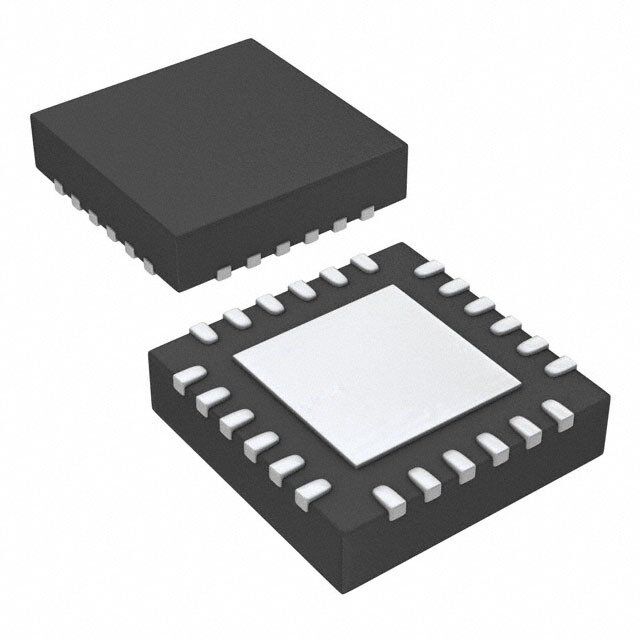
| 供应商器件封装 | 24-QFN |
| 其它名称 | 497-14029-2 |
| 内部驱动器 | 是 |
| 包装 | 带卷 (TR) |
| 商标 | STMicroelectronics |
| 安装类型 | 表面贴装 |
| 安装风格 | SMD/SMT |
| 封装 | Reel |
| 封装/外壳 | 24-VFQFN 裸露焊盘 |
| 封装/箱体 | QFN-24 |
| 工作温度 | -40°C ~ 85°C |
| 工作频率 | 30 MHz |
| 工厂包装数量 | 4000 |
| 恒压 | - |
| 恒流 | 是 |
| 拓扑 | 低端,PWM |
| 最大工作温度 | + 85 C |
| 最大电源电流 | 10 mA |
| 最小工作温度 | - 40 C |
| 标准包装 | 4,000 |
| 电压-电源 | 3 V ~ 5.5 V |
| 电压-输出 | 19V |
| 类型-初级 | 通用 |
| 类型-次级 | - |
| 系列 | LED1642GW |
| 输入电压 | 3.3 V |
| 输出数 | 16 |
| 输出电流 | 50 mA |
| 配用 | /product-detail/zh/STEVAL-ILL061V1/497-14466-ND/4738917 |
| 频率 | - |


- 商务部:美国ITC正式对集成电路等产品启动337调查
- 曝三星4nm工艺存在良率问题 高通将骁龙8 Gen1或转产台积电
- 太阳诱电将投资9.5亿元在常州建新厂生产MLCC 预计2023年完工
- 英特尔发布欧洲新工厂建设计划 深化IDM 2.0 战略
- 台积电先进制程称霸业界 有大客户加持明年业绩稳了
- 达到5530亿美元!SIA预计今年全球半导体销售额将创下新高
- 英特尔拟将自动驾驶子公司Mobileye上市 估值或超500亿美元
- 三星加码芯片和SET,合并消费电子和移动部门,撤换高东真等 CEO
- 三星电子宣布重大人事变动 还合并消费电子和移动部门
- 海关总署:前11个月进口集成电路产品价值2.52万亿元 增长14.8%


PDF Datasheet 数据手册内容提取
LED1642GW 16 channel LED driver with error detection current gain control and 12/16-bit PWM brightness control Datasheet - production data Applications • Full color/monochrome large displays • LED signage QSOP-24 Description The LED1642GW is a monolithic, low voltage, low current power 16-bit shift register designed for LED panel displays. The LED1642GW TSSOP24 guarantees 20 V output driving capability allowing TSSOP24 (exposed pad) the user to connect several LEDs in series. In the output stage, sixteen regulated current sources provide from 3 mA to 40 mA constant current to drive the LEDs. The current is programmed Features through an external resistor and can be adjusted by a 7-bit current gain register in two subranges. • 16 constant current output channels The brightness can be adjusted separately for • Output current: from 3 mA to 40 mA each channel through 12/16-bit grayscale control. • Current programmable through external Programmable turn-on and turn-off time (four resistor different values available) improves the low noise • 7-bit global current gain adjustment in two generation performance of the system. ranges Open/short error detection mode is available in • 12/16-bit PWM grayscale brightness control the LED1642GW. The auto power-shutdown and • Programmable output turn-on/off time auto power-on features (selectable) allow the device to save power without external • Error detection mode (both open and shorted- intervention. LED) Thermal management includes an • Programmable shorted-LED detection overtemperature data alert and output thermal thresholds shutdown (170 °C). The high clock frequency is • Auto power saving/auto-wakeup up to 30 MHz and it makes the device suitable for • Selectable SDO synchronization on the CLK high data rate transmission. A selectable gradual falling edge output delay reduces the inrush current, whereas the selectable SDO synchronization feature works • Gradual output delay (selectable) when the device is used in daisy-chain • Supply voltage: 3 V to 5.5 V configuration. The supply voltage range is • Thermal shutdown and overtemperature alert between 3 V and 5.5 V. • 30 MHz 4-wires interface • 20 V current generator rated voltage November 2015 DocID024395 Rev 6 1/42 This is information on a product in full production. www.st.com
Contents LED1642GW Contents 1 Pin description . . . . . . . . . . . . . . . . . . . . . . . . . . . . . . . . . . . . . . . . . . . . . 6 2 Absolute maximum ratings . . . . . . . . . . . . . . . . . . . . . . . . . . . . . . . . . . . 7 3 Thermal characteristics . . . . . . . . . . . . . . . . . . . . . . . . . . . . . . . . . . . . . . 8 4 Electrical characteristics . . . . . . . . . . . . . . . . . . . . . . . . . . . . . . . . . . . . . 8 5 Switching characteristics . . . . . . . . . . . . . . . . . . . . . . . . . . . . . . . . . . . . 12 6 Simplified internal block diagram . . . . . . . . . . . . . . . . . . . . . . . . . . . . . 15 6.1 Equivalent circuits of inputs and outputs . . . . . . . . . . . . . . . . . . . . . . . . . 15 7 Digital blocks . . . . . . . . . . . . . . . . . . . . . . . . . . . . . . . . . . . . . . . . . . . . . . 16 8 Configuration register . . . . . . . . . . . . . . . . . . . . . . . . . . . . . . . . . . . . . . . 18 8.1 Gain control (from CFG 0 to 5) and current ranges (CFG- 6) . . . . . . . . . 19 8.2 Error detection mode (CFG-7) . . . . . . . . . . . . . . . . . . . . . . . . . . . . . . . . . 21 8.3 Error detection conditions . . . . . . . . . . . . . . . . . . . . . . . . . . . . . . . . . . . . . 24 8.4 Auto-wakeup/auto power shutdown (CFG-10) . . . . . . . . . . . . . . . . . . . . . 24 8.5 Programmable turn-on/turn-off time (CFG-11/12) . . . . . . . . . . . . . . . . . . 24 8.6 SDO delay (CFG-13) . . . . . . . . . . . . . . . . . . . . . . . . . . . . . . . . . . . . . . . . 25 8.7 Gradual output delay (CFG-14) . . . . . . . . . . . . . . . . . . . . . . . . . . . . . . . . 26 8.8 PWM counter setting and brightness register (CFG-15) . . . . . . . . . . . . . 27 9 Thermal flag . . . . . . . . . . . . . . . . . . . . . . . . . . . . . . . . . . . . . . . . . . . . . . . 29 10 Dropout voltage . . . . . . . . . . . . . . . . . . . . . . . . . . . . . . . . . . . . . . . . . . . . 30 2/42 DocID024395 Rev 6
LED1642GW Contents 11 Package information . . . . . . . . . . . . . . . . . . . . . . . . . . . . . . . . . . . . . . . . 31 11.1 QSOP-24 package information . . . . . . . . . . . . . . . . . . . . . . . . . . . . . . . . 32 11.2 QFN-24 package information . . . . . . . . . . . . . . . . . . . . . . . . . . . . . . . . . . 34 11.3 TSSOP24 package information . . . . . . . . . . . . . . . . . . . . . . . . . . . . . . . . 36 11.4 TSSOP24 exposed pad package information . . . . . . . . . . . . . . . . . . . . . 37 11.5 TSSOP24 and TSSOP24 exposed pad packing information . . . . . . . . . . 39 12 Ordering information . . . . . . . . . . . . . . . . . . . . . . . . . . . . . . . . . . . . . . . 40 13 Revision history . . . . . . . . . . . . . . . . . . . . . . . . . . . . . . . . . . . . . . . . . . . 41 DocID024395 Rev 6 3/42 42
List of tables LED1642GW List of tables Table 1. Pin description . . . . . . . . . . . . . . . . . . . . . . . . . . . . . . . . . . . . . . . . . . . . . . . . . . . . . . . . . . . 6 Table 2. Absolute maximum ratings. . . . . . . . . . . . . . . . . . . . . . . . . . . . . . . . . . . . . . . . . . . . . . . . . . 7 Table 3. Thermal characteristics. . . . . . . . . . . . . . . . . . . . . . . . . . . . . . . . . . . . . . . . . . . . . . . . . . . . . 8 Table 4. Electrical characteristics. . . . . . . . . . . . . . . . . . . . . . . . . . . . . . . . . . . . . . . . . . . . . . . . . . . . 8 Table 5. Switching characteristics . . . . . . . . . . . . . . . . . . . . . . . . . . . . . . . . . . . . . . . . . . . . . . . . . . 12 Table 6. Programmable TON/TOFF (output rise and fall time). . . . . . . . . . . . . . . . . . . . . . . . . . . . . 13 Table 7. Digital key summary. . . . . . . . . . . . . . . . . . . . . . . . . . . . . . . . . . . . . . . . . . . . . . . . . . . . . . 16 Table 8. Configuration register. . . . . . . . . . . . . . . . . . . . . . . . . . . . . . . . . . . . . . . . . . . . . . . . . . . . . 18 Table 9. Example of current ranges . . . . . . . . . . . . . . . . . . . . . . . . . . . . . . . . . . . . . . . . . . . . . . . . . 20 Table 10. Gain steps for the current range selected by REXT = 11 kW. . . . . . . . . . . . . . . . . . . . . . . 20 Table 11. Diagnostic thresholds. . . . . . . . . . . . . . . . . . . . . . . . . . . . . . . . . . . . . . . . . . . . . . . . . . . . . 24 Table 12. Minimum dropout voltage for some current values. . . . . . . . . . . . . . . . . . . . . . . . . . . . . . . 30 Table 13. QSOP-24 mechanical data. . . . . . . . . . . . . . . . . . . . . . . . . . . . . . . . . . . . . . . . . . . . . . . . . 33 Table 14. QFN-24 mechanical data . . . . . . . . . . . . . . . . . . . . . . . . . . . . . . . . . . . . . . . . . . . . . . . . . . 35 Table 15. TSSOP24 mechanical data . . . . . . . . . . . . . . . . . . . . . . . . . . . . . . . . . . . . . . . . . . . . . . . . 36 Table 16. TSSOP24 exposed pad mechanical data. . . . . . . . . . . . . . . . . . . . . . . . . . . . . . . . . . . . . . 38 Table 17. TSSOP24 and TSSOP24 exposed pad tape and reel mechanical data. . . . . . . . . . . . . . . 39 Table 18. Ordering information. . . . . . . . . . . . . . . . . . . . . . . . . . . . . . . . . . . . . . . . . . . . . . . . . . . . . . 40 Table 19. Document revision history . . . . . . . . . . . . . . . . . . . . . . . . . . . . . . . . . . . . . . . . . . . . . . . . . 41 4/42 DocID024395 Rev 6
LED1642GW List of figures List of figures Figure 1. TSSOP24, TSSOP24EP, QSOP-24 pinout . . . . . . . . . . . . . . . . . . . . . . . . . . . . . . . . . . . . . 6 Figure 2. QFN-24 pinout . . . . . . . . . . . . . . . . . . . . . . . . . . . . . . . . . . . . . . . . . . . . . . . . . . . . . . . . . . . 6 Figure 3. Typical chip-to-chip accuracy. . . . . . . . . . . . . . . . . . . . . . . . . . . . . . . . . . . . . . . . . . . . . . . 10 Figure 4. Typical application schematic. . . . . . . . . . . . . . . . . . . . . . . . . . . . . . . . . . . . . . . . . . . . . . . 11 Figure 5. Timing for clock, serial in, serial out, latch enable and outputs. . . . . . . . . . . . . . . . . . . . . . 14 Figure 6. LED1642GW simplified block diagram. . . . . . . . . . . . . . . . . . . . . . . . . . . . . . . . . . . . . . . . 15 Figure 7. Input and output equivalent circuits . . . . . . . . . . . . . . . . . . . . . . . . . . . . . . . . . . . . . . . . . . 15 Figure 8. Digital keys. . . . . . . . . . . . . . . . . . . . . . . . . . . . . . . . . . . . . . . . . . . . . . . . . . . . . . . . . . . . . 17 Figure 9. Channel data and write switch . . . . . . . . . . . . . . . . . . . . . . . . . . . . . . . . . . . . . . . . . . . . . . 17 Figure 10. Channel current vs. gain register value . . . . . . . . . . . . . . . . . . . . . . . . . . . . . . . . . . . . . . . 21 Figure 11. Error detection action sequence. . . . . . . . . . . . . . . . . . . . . . . . . . . . . . . . . . . . . . . . . . . . . 22 Figure 12. Error detection power-on timing . . . . . . . . . . . . . . . . . . . . . . . . . . . . . . . . . . . . . . . . . . . . . 22 Figure 13. Configuration register reading sequence . . . . . . . . . . . . . . . . . . . . . . . . . . . . . . . . . . . . . . 23 Figure 14. Configuration register reading sequence (zoom) . . . . . . . . . . . . . . . . . . . . . . . . . . . . . . . . 23 Figure 15. Configuration register reading sequence - SDO delay actives. . . . . . . . . . . . . . . . . . . . . . 23 Figure 16. Configuration register reading sequence - SDO delay actives (zoom). . . . . . . . . . . . . . . . 23 Figure 17. Output TON (current rise time) CFG -12 = CFG - 11 = 0 . . . . . . . . . . . . . . . . . . . . . . . . . . 25 Figure 18. Output TOFF (current fall time) CFG - 2 = CFG - 11 = 0 . . . . . . . . . . . . . . . . . . . . . . . . . . 25 Figure 19. Output TON (current rise time) CFG -12 = CFG - 11 = 1 . . . . . . . . . . . . . . . . . . . . . . . . . . 25 Figure 20. Output TOFF (current fall time) CFG -12 = CFG - 11 = 1. . . . . . . . . . . . . . . . . . . . . . . . . . 25 Figure 21. SDO delay . . . . . . . . . . . . . . . . . . . . . . . . . . . . . . . . . . . . . . . . . . . . . . . . . . . . . . . . . . . . . 26 Figure 22. Gradual output delay . . . . . . . . . . . . . . . . . . . . . . . . . . . . . . . . . . . . . . . . . . . . . . . . . . . . . 27 Figure 23. PWCLK counter and comparator . . . . . . . . . . . . . . . . . . . . . . . . . . . . . . . . . . . . . . . . . . . . 28 Figure 24. Brightness register setting . . . . . . . . . . . . . . . . . . . . . . . . . . . . . . . . . . . . . . . . . . . . . . . . . 28 Figure 25. Thermal flag status. . . . . . . . . . . . . . . . . . . . . . . . . . . . . . . . . . . . . . . . . . . . . . . . . . . . . . . 29 Figure 26. Typical channel dropout voltage vs. output current (VDD = 3.3 V). . . . . . . . . . . . . . . . . . . 30 Figure 27. QSOP-24 package outline . . . . . . . . . . . . . . . . . . . . . . . . . . . . . . . . . . . . . . . . . . . . . . . . . 32 Figure 28. QFN-24 package outline. . . . . . . . . . . . . . . . . . . . . . . . . . . . . . . . . . . . . . . . . . . . . . . . . . . 34 Figure 29. TSSOP24 package outline. . . . . . . . . . . . . . . . . . . . . . . . . . . . . . . . . . . . . . . . . . . . . . . . . 36 Figure 30. TSSOP24 exposed pad outline . . . . . . . . . . . . . . . . . . . . . . . . . . . . . . . . . . . . . . . . . . . . . 37 Figure 31. TSSOP24 and TSSOP24 exposed pad tape and reel outline . . . . . . . . . . . . . . . . . . . . . . 39 DocID024395 Rev 6 5/42 42
Pin description LED1642GW 1 Pin description Figure 1. TSSOP24, TSSOP24EP, QSOP-24 pinout GND VDD SDI R-EXT CLK SDO LE PWCLK OUT0 OUT15 OUT1 OUT14 OUT2 OUT13 OUT3 OUT12 OUT4 OUT11 OUT5 OUT10 OUT6 OUT9 OUT7 OUT8 AM13686v1 Figure 2. QFN-24 pinout T CLK SDI GND VDD R-EX SDO 24 23 22 21 20 19 LE 1 18 PWCLK OUT0 2 17 OUT15 OUT1 3 16 OUT14 OUT2 4 15 OUT13 OUT3 5 14 OUT12 OUT4 6 13 OUT11 7 8 9 10 11 12 UT5 UT6 UT7 UT8 UT9 T10 O O O O O U O AM13687V1 Table 1. Pin description TSSOP24 TSSOP24EP QFN-24 Symbol Name and function QSOP-24 1 22 GND Ground terminal 2 23 SDI Serial data input terminal 3 24 CLK Clock input terminal 4 1 LE Latch input terminal 5-20 2-17 OUT0-OUT15 Output terminals 21 18 PWCLK Clock input for PWM counter 6/42 DocID024395 Rev 6
LED1642GW Absolute maximum ratings Table 1. Pin description (continued) TSSOP24 TSSOP24EP QFN-24 Symbol Name and function QSOP-24 22 19 SDO Serial data output terminal Terminal for external resistor for constant current 23 20 R-EXT programming 24 21 VDD Supply voltage terminal 2 Absolute maximum ratings Stressing the device above the ratings listed in the Table2 may cause the device permanent damage. Operating under conditions above those indicated in the operating section is not implied. Exposure to absolute maximum rating conditions for extended periods may affect the device reliability. Table 2. Absolute maximum ratings Symbol Parameter Value Unit V Supply voltage 0 to 7 V DD V Output voltage -0.5 to 20 V OUT I Output current 50 mA OUT V Input voltage -0.4 to V +0.4 V i DD I GND terminal current 1400 mA GND Electrostatic discharge protection ESD ±2 kV HBM human body model DocID024395 Rev 6 7/42 42
Thermal characteristics LED1642GW 3 Thermal characteristics Table 3. Thermal characteristics Symbol Parameter Value Unit T Operative free-air temperature range(1) -40 to +85 a T Operative junction temperature range -40 to +125 °C OPR T Storage ambient temperature range -55 to +150 STG QFN-24(2) 30 TSSOP24 85 R Thermal resistance junction-ambient °C/W thj-amb TSSOP24EP(2) 37.5 QSOP-24 72 1. This data must be considered in adequate power dissipation conditions, the junction temperature must be maintained below 125 °C. 2. The exposed pad should be soldered directly to the PCB to get the thermal benefits. The exposed pad can be attached to a metal land electrically isolated or connected to ground. 4 Electrical characteristics V = 3.3 V, T = 25 °C, unless otherwise specified. DD j Table 4. Electrical characteristics Symbol Parameter Conditions Min. Typ. Max. Unit V Supply voltage 3 5.5 DD V Output voltage Out 0 - out 15 - - 19 OUT V 0.7 x V - V IH DD DD Input voltage V V GND - 0.3 x V IL DD VOL Serial data output voltage VDD= 3 to 5.5 V - - 0.4 V (SDO) I = +/- 1 mA V -0.4 - - OH DD I Output leakage current V = 19 V, all outputs OFF - - 0.5 µA Oleak OUT UVLO threshold (rising) 2.7 2.9 V V uvlo UVLO threshold (falling) 2.2 2.3 Hy UVLO hysteresis 400 mV uvlo 8/42 DocID024395 Rev 6
LED1642GW Electrical characteristics Table 4. Electrical characteristics (continued) Symbol Parameter Conditions Min. Typ. Max. Unit V = 0.1 V; (I = 3 mA) OUT OUT R = 11 kΩ EXT ∆I - - ±4 OL1 CFG-0…CFG-5= “000000” CFG-6 = “0” V = 0.5 V; (I = 20 mA) OUT OUT Output current precision R = 11 kΩ ∆I channel-to-channel EXT - - ±3 % OL2 CFG-0…CFG-5 = “011010” (all outputs ON)(1)(2) CFG-6 = “1” V = 0.8 V; (I = 36 mA) OUT OUT R = 11 kΩ EXT ∆I - - ±3 OL3 CFG-0…CFG-5 = “111111” CFG-6 = “1” V = 0.5 V; (I = 20 mA) OUT OUT Output current precision R =1 1 kΩ ∆I device-to-device EXT - - ±6 % OL2a CFG-0…CFG-5 = “011010” (all outputs ON)(1) CFG-6 = “1” V from 1 V to 3 V; (I = OUT OUT Output current vs. output 36 mA) REXT = 11 kΩ %/dV - ±0.1 - OUT voltage regulation (3) CFG-0…CFG-5 = “111111” CFG-6 = “1” V from 3 V to 5.5 V %/V DD V = 0.8 V; (I = 36 mA) OUT OUT Output current vs. supply %/dV R = 11 kΩ - ±1 - DD voltage regulation(4) EXT CFG-0…CFG-5 = “111111” CFG-6 = “1” Pull-up resistor for PWCLK Rup 400 500 600 pin Rdw Pull-down resistor for LE pin 400 500 600 KΩ External current setup R 100 EXT resistance R = 11 kΩ EXT I (OFF1) Supply current (OFF) OUT 0 to 15 = OFF - - 6 DD CFG = default R = 11 kΩ; I = 20 mA EXT OUT OUT 0 to 15 = ON I (ON1) - 8 DD CFG-0…CFG-5 = “011010” mA CFG-6 = “1” Supply current (ON) R = 11 kΩ; I = 36 mA EXT OUT OUT 0 to 15 = ON I (ON2) - 10 DD CFG-0…CFG-5 = “111111” CFG-6 = “1” DocID024395 Rev 6 9/42 42
Electrical characteristics LED1642GW Table 4. Electrical characteristics (continued) Symbol Parameter Conditions Min. Typ. Max. Unit R = 11 kΩ; EXT I (auto OUT 0 to 15 = OFF DD Supply current (auto OFF) - 200 500 µA OFF) CFG-0…CFG-5 = “111111” CFG-6 = “1” T Thermal flag 150 flg T Thermal shutdown(5) 170 sd °C Thermal shutdown T 15 20 sd-hy hysteresis(5) 1. Tested with just one output loaded. 2. ((Ioutn - Ioutavg1-15)/ Ioutavg1-15) x 100. 3. Δ(%/V)= (Ioutn@Voutn=3.0V)−(Ioutn@Voutn=1.0V)×100 (Ioutn@Voutn=1.0V) 3−1 4. Δ(%/V) = (Ioutn@Vdd= 5.5V) −(Ioutn@Vdd =3.0V) × 100 (Ioutn@Vdd =3.0V) 5.5−3 5. Not tested, guaranteed by design. Figure 3. Typical chip-to-chip accuracy VDD=3.3/5 V; T=25 ° C 4 3.5 3 %) p ( 2.5 hi c 2 o- p-t 1.5 hi C 1 0.5 0 0 5 10 15 20 25 30 35 40 IOUT (mA) AM13688V1 10/42 DocID024395 Rev 6
LED1642GW Electrical characteristics Figure 4. Typical application schematic LED common rail voltage + Cled ….. Supply voltage VDD OUT0 OUT1 OUT15 SDI Data loaded Cin CLK through serial interface LED1642GW LE PWCLK R-EXT SDO Data output GND Current setting resistor AM13689V1 DocID024395 Rev 6 11/42 42
Switching characteristics LED1642GW 5 Switching characteristics V = 3.3 V, T = 25 °C, unless otherwise specified. DD j Table 5. Switching characteristics(1) Symbol Parameter Conditions Min. Typ. Max. Unit f Clock frequency Cascade operation - - 30 clk MHz f PWclock frequency - - 30 pwclk R = 11 kΩ; I = 20 mA tr SDO rise time EXT OUT - 5 - (SDO) V = 0.8 V OUT VIH = V ; VIL = GND DD RL = 3.3 KΩ; CL = 10 pF tf SDO fall time - 5 - (SDO) CFG-0…CFG-5 = “011010” CFG-6 = “1” tPLHLE LE - OUTn(2) Propagation delay - 200 - time CLK - SDO tPLH 8 15 25 CFG-13 = ‘0’ (“L to “H”) tPHLLE LE - OUTn(2) Propagation delay - 100 - time CLK - SDO ns tPHL (“H” to “L”) 8 15 25 CFG-13 = ‘0’ R = 11 kΩ; I = 20 mA tw(CLK) CLK EXT OUT 20 - - V = 0.8 V OUT t (PWCLK) PWCLK Pulse width 20 - - W VIH = V ; VIL = GND DD tw(L) LE RL = 50 Ω; CL = 10 pF 20 - - CFG-0…CFG-5 = “011010” t Gradual delay ch-to-ch 10 gr-d CFG-6 = “1” t Setup time for LE 5 - - su(L) t Hold time for LE 5 - - h(L) t Setup time for SDI 5 - - su(D) t Hold time for SDI 10 - - h(D) tclkr(3) Maximum CLK rise time - - 5 µs tclkf(3) Maximum CLK fall time - - 5 V = 0.6 to 3 V I Output current turn-on overshoot OUT - - 10 % out-ov CL = 10 pF; I = 3 to 36 mA OUT Normal error detection t - - 1 µs n-err minimum output ON time 12/42 DocID024395 Rev 6
LED1642GW Switching characteristics Table 5. Switching characteristics(1) Symbol Parameter Conditions Min. Typ. Max. Unit From LE falling edge to R t Auto power shutdown time (auto OFF) EXT - 100 - ns shutdown voltage reference at -10% From LE falling edge to R t Auto-wakeup EXT - 3 - µs wakeup voltage reference at 90% 1. Not tested in production. All table limits are guaranteed by design. 2. CFG -11= 0 and CFG -12 = 0 (output tr = 30 ns; output tf = 20 ns); CFG-14=1 (no output gradual delay). 3. If devices are connected in cascade and tclkr or tclkf is large, it may be critical to achieve the timing required for data transfer between two cascaded devices. Table 6. Programmable T /T (output rise and fall time) ON OFF Typ. (20% to 80%) Configuration bits Conditions Unit (CFG-12 - CFG-11) Turn-on Turn-off 0 - 0 R = 11 kΩ; I = 20 mA 30 ns 20 ns EXT OUT V = 0.8 V 0 - 1 OUT 100 ns 40 ns VIH= V ; VIL= GND 1 - 0 DD 140 ns 80 ns ns RL = 50 Ω; CL=10pF CFG-0...CFG-5=“011010” 1 - 1 180 ns 150 ns CFG-6 = “1” DocID024395 Rev 6 13/42 42
Switching characteristics LED1642GW Figure 5. Timing for clock, serial in, serial out, latch enable and outputs t ,t pLHLE pHLLE AM13690V1 The correct sampling of the data depends on the stability of the data at SDI on the rising edge of the clock signal and it is assured by a proper data setup and hold time (t and SU(D) t ), as shown in Figure5. The same figure shows the propagation delay from CLK to SDO h(D) (t /t ). Figure5 describes also the minimum duration of CLK, LE pulses (t ) and PLH PHL W(CLK) t respectively and the propagation delay from LE to OUT (t and t ) in the W(L) n PLHLE PHLLE hypothesis that all channels have already been enabled by PWM counter. 14/42 DocID024395 Rev 6
LED1642GW Simplified internal block diagram 6 Simplified internal block diagram Figure 6. LED1642GW simplified block diagram SDO PWCLK SDI Control Logic & OUT0 CLK PWM Data Registers LE counter OUT1 VDD UVLO Error GND & POR detection OUT2 … Thermal Configuration shutdown 16 … register o … u tp … u t c h OUT14 Channel driver a R-EXT CuRrreefn.t Caudrjruesnttm geanint Timing control nne Turn ON/OFF ls OUT15 Gradual delay AM13691V1 6.1 Equivalent circuits of inputs and outputs LE and PWCLK input terminals have pull-down and pull-up connection respectively. CLK and SDI must be connected to the external circuit to fix the logic level. Figure 7. Input and output equivalent circuits PWCLK terminal LE terminal CLK, SDI terminal SDO terminal AM13692V1 DocID024395 Rev 6 15/42 42
Digital blocks LED1642GW 7 Digital blocks The data input arrives through the serial Interface at each CLK rising edge. The LE signal is used to latch the loaded data and also to address data loading to the appropriate register, thermal flag reading and error detection. The access to the different registers or functions of the device (configuration register, brightness register or current gain, error detection, etc.) is achieved by using different digital keys, defined as a number of CLK pulses during which the LE signal is asserted. The available digital keys are listed in Table7 and Figure8. A typical channel data input is shown in Figure9. Table 7. Digital key summary Number # CLK rising edge when the LE is “1” Command description 1 1 – 2 Write switch (to turn on/off output channels) 2 3 – 4 Brightness data latch 3 5 – 6 Brightness global latch 4 7 Write configuration register 5 8 Read configuration register 6 9 Start open error detection mode 7 10 Start short error detection mode 8 11 Start combined error detection mode 9 12 End error detection mode 10 13 Thermal error reading 11 14 Reserved 12 15 Reserved 16/42 DocID024395 Rev 6
LED1642GW Digital blocks Figure 8. Digital keys CLK LE Write switch LE Data latch LE Global latch LE Write CR LE Read CR LE Start open error detection LE Start short error detection LE Start combined detection LE End error detection LE Thermal error reading AM13693V1 Figure 9. Channel data and write switch SDI 0F 0E 0D 0C 0B 0A 09 08 07 06 05 04 03 02 01 00 CLK LE 16-bit data AM13694V1 DocID024395 Rev 6 17/42 42
Configuration register LED1642GW 8 Configuration register The configuration register is used to enable or disable some device features, to program some parameters and to change other settings. The access to this register (read or write) is managed to find a description for each bit as described in Table8. The default value of the configuration register (when the device is switched on or after a reset) is "0" for all bits. To change anything in the configuration register, a 16-bit digital word must be sent (CFG - 0 represents LSB, CFG -15 the MSB). Table 8. Configuration register Bit Definition R/W Description Default CFG-0 0 CFG-1 0 CFG-2 0 Current gain 6-bit DAC allows adjusting the device output current in 64 R/W CFG-3 adjustment steps for each range (defined by CFG-6) 0 CFG-4 0 CFG-5 0 ”0” low current range CFG-6 Current range R/W 0 “1” high current range Error detection “0” normal mode CFG-7 R/W 0 mode “1” reserved mode CFG-9 CFG-8 Th. volt. CFG-8 R/W 0 0 1.8 V 0 Shorted-LED Programmable output detection shorted-LED detection 0 1 2.5 V thresholds thresholds 1 0 3 V CFG-9 R/W 0 1 1 3.5 V Auto OFF “0” device always ON CFG-10 R/W 0 shutdown ”1” auto power shutdown active (auto OFF) CFG-12 CFG-11 Turn-on Turn-off CFG-11 R/W 0 0 30 ns 20 ns 0 Programmable Output turn- output rise and fall 0 1 100 ns 40 ns on/off time time (20% to 80%) 1 0 140 ns 80 ns CFG-12 R/W 0 1 1 180 ns 150 ns If “0” no delay is present on SDO CFG-13 SDO delay R/W If “1” the data are shifted out and they are synchronized with 0 the falling edge of the CLK signal 18/42 DocID024395 Rev 6
LED1642GW Configuration register Table 8. Configuration register (continued) Bit Definition R/W Description Default “0” a progressive delay is applied to output (10 ns per Gradual output CFG-14 R/W channel) 0 delay ”1” no delay is applied to output “0” to select 16-bit brightness register (65536 grayscale 12/16 PWM rightness steps). CFG-15 R/W 0 counter “1” to select 12-bit brightness register (4096 grayscale brightness steps) 8.1 Gain control (from CFG 0 to 5) and current ranges (CFG- 6) The LED current can be programmed using an external resistor connected to GND from R pin and can be fixed using the dedicated bits of the configuration register (from CFG - EXT 0 to CFG - 5 bits define the gain, while CFG - 6 bit defines the current range within the which the gain can be adjusted). The device can regulate the current up to 36 mA and down to 0.5 mA. The accuracy of the LED current depends on the selected range and it is guaranteed in the ranges indicated in the static electrical characteristics only (see Table3 and 9). When the device is switched on, the selected current range and the resistor connected to the R EXT pin fix the default LED current: V I = REF ⋅K OL_default R EXT Where V =1.23 V is the voltage of the R pin and K is the mirroring current ratio, whose REF EXT value depends on the selected current range: • K = 28 with low current range selected (CFG - 6 = "0") • K = 80 with high current range selected (CFG - 6 = "1") The relation between the programmed current and the current gain settings is the following: I = (I + G ⋅ΔI ) OL OL_default step where G is the current gain value (decimal value) defined by the dedicated bits of the current gain register. The current gain is managed by 6-bits of the configuration register (CFG - 0 to CFG - 5, CFG - 0 is LSB and CFG - 5 is MSB) and can be adjusted within two ranges (selectable through the bit CFG - 6) over 64 steps. The width of each step depends on the default current (I ) as well as the selected R . Finally, each step is as ol_default EXT follows: DocID024395 Rev 6 19/42 42
Configuration register LED1642GW I ΔI = OL_default step 21 The Table9 shows an example of the current setting with an external resistance (R ) = 11 EXT KΩ: Table 9. Example of current ranges R [KΩ] CFG-6 CFG-0 to CFG-5 LED current(1) [mA] Accuracy EXT 11 0 000000 3.1 mA ± 4% ch-to-ch Low range 11 0 111111 12.5 mA - 11 1 000000 8.9 mA High range 11 1 011010 20 mA ± 3% ch-to-ch 1. The indicated values may be slightly different on the current device. The Table10 shows an example of current setting and gain control with R = 11 kΩ, see EXT also Figure10. Table 10. Gain steps for the current range selected by R = 11 kΩ EXT CFG-6 CFG(0 to 5) LED current (1) [mA] 0 000000 3.131 0 000001 3.280 Low range … … … 0 111111 12.524 1 000000 8.945 1 000001 9.371 High range … … … 1 111111 35.78 1. The indicated values may be slightly different on the current device. The external programming resistance must be connected as close as possible to the related device pins (R and GND) to reduce as minimum as possible the routing length and EXT prevent reference noise injection and electromagnetic interferences. Moreover, a direct connection to the device GND pin reduces the possible output current variation when the total device ground current changes (load effect). 20/42 DocID024395 Rev 6
LED1642GW Configuration register Figure 10. Channel current vs. gain register value IOOUUTT vs. gain (R = range selection, REXT = 11 K or 18 K) 40.0 35.0 11 KR=0 11 KR=1 30.0 18 KR=0 18 KR=1 )) 25.0 AA mm ( (TT 20.0 UU IOO 15.0 10.0 5.0 0.0 0 5 10 15 20 25 30 35 40 45 50 55 60 65 70 Gain register decimal value AM13695V1 8.2 Error detection mode (CFG-7) Stopping the normal activity of the display and turning on all driver channels allows the error detection to be performed and failed LED or display defects to be checked. The error detection is active when the CFG -7 bit of the configuration register is "0". The diagnostics is performed as shown in Figure11: • The LED has to be selected turning on the relative channel on the switch register (powering on or off the output channels); the brightness register value for this channel cannot be zero. • The normal error detection has to be selected in the configuration register (CFG-7= "0"). The appropriate digital key to choose the type of detection (open, short or combined) must be sent (see Table7). • After the error detection starts, the channel under testing has to be turned on at least 1 μ s (the LED is at the nominal current). Please note that, the output power-on depends on PWCLK signal and in several applications this signal is not synchronized with the serial interface clock (CLK pin). Therefore, to be sure that, between the detection start μ and the detection end, the output power-on is 1 s and moreover, that last power-on, in μ the interval, starts at least 0.5 s before the detection end pattern (see Figure12), it is suggested that the error detection should be performed just after the device startup (brightness counter reset) with all channels ON, before applying PWCLK signal. • The result of the detection ("0" indicates a fault condition) is shifted out SDO, in 16 clock pulses after the "detection end command" is provided, first output bit represents channel 15 (error data can be read in a way similar to configuration register data reading as shown on Figure13, 14, 15 and 16). Please note that (with SDO delay off) output 15 detection result will be available just after 1st clock pulse rising edge, so it can be sampled on the rising edge of second clock pulse. In the same way output 0 detection result will be available just after 16th clock pulse rising edge, so it can be sampled on the rising edge of 17th CLK pulse. DocID024395 Rev 6 21/42 42
Configuration register LED1642GW Figure 11. Error detection action sequence Normal detection sequence Select LED to be turned on and checked in switch register data; brightness for selected channels cannot be zero. Select normal error detection mode on CFG register (bit 7 = “0”) Send open, short or combined error detection start command by LE digital keys Turn on LED by PWCLK pulses for at least 1 µ s Send error detection end command by LE digital key Read error detection result on SDO in 16 clock pulses after detection end command AM13696V1 Figure 12. Error detection power-on timing x0000 < BRT < xFFFF Output Current 1us 0.5us Det. Det. Start End SPI pattern It must contain 1us output power ON AM13697V1 22/42 DocID024395 Rev 6
LED1642GW Configuration register Figure 13. Configuration register reading Figure 14. Configuration register reading sequence sequence (zoom) CCC213===SCLEDLKI Faifrtsetr C CLFKG p Ruelsge CCC213===SCLEDLKI C4=SDO reading command C4=SDO CFG Regprogramming CFG Regreading command CFG Regdata CFG Regdata First CLK pulse after CFG Reg reading command Figure 15. Configuration register reading Figure 16. Configuration register reading sequence - SDO delay actives sequence - SDO delay actives (zoom) C1=CLK C1=CLK C2=SDI Sync. change First CLK pulse C2=SDI CC43==SLEDO reaafdtienrg C cFoGm Rmeagnd CC43==SLEDO CFG Regprogramming CFG Regreading command CFG Regdata CFG13=1 CFG Regdata First CLK pulse after CFG Reg reading command DocID024395 Rev 6 23/42 42
Configuration register LED1642GW 8.3 Error detection conditions During the error detection phases for each channel, the following checks have to be performed: – The output current in open detection mode (digital key: 9 CLK rising edges when LE is "1") – The output voltage in short detection (digital key: 10 CLK rising edges when LE is "1") – Both parameters (output voltage and current) in combined error detection mode (digital key: 11 CLK rising edges when LE is "1"). The thresholds for the error diagnostics are listed in Table11: Table 11. Diagnostic thresholds Thresholds (V) Error detection Checked CFG-9 CFG-8 modes malfunction Min. Typ. Max. Open Open line or output I ≤ 0.5 x I x x - OUT OUT - detection e short to GND programmed d o m 0 0 1.15 V ≥ 1.8 2.05 d OUT e Short bin Short on LED or short 0 1 2.25 VOUT ≥ 2.5 2.75 detection om to V-LED 1 0 2.75 VOUT ≥ 3.0 3.25 C 1 1 3.25 V ≥ 3.5 3.80 OUT 8.4 Auto-wakeup/auto power shutdown (CFG-10) This feature reduces the power consumption when all outputs are OFF. It is active when the CFG -10 bit of configuration register is "1". The auto power shutdown (auto OFF) starts when the data latched is "0" for all channels, and device is active again (wakeup) at the first latched data string including at least one bit = "1" (at least one channel ON). Timings for shutdown and wakeup are present in the dynamics feature table. While the auto power shutdown is active, the device ignores any other command except the channel power-on. 8.5 Programmable turn-on/turn-off time (CFG-11/12) The device gives the possibility to program the turn-on and turn-off time of the current generators. Four different values can be selected using CFG -12 and CFG-11 bits of the configuration register (see Table8) to fit the application requirements: 30/20 ns (00), 100/40 ns (01), 140/80 ns (10) and 180/150 ns (11). The selected value refers to T (current rise ON time) and T (current fall time). OFF 24/42 DocID024395 Rev 6
LED1642GW Configuration register Figure 17. Output T (current rise time) CFG - Figure 18. Output T (current fall time) CFG - ON OFF 12 = CFG - 11 = 0 2 = CFG - 11 = 0 AM13698V1 AM13699V1 Figure 19. Output T (current rise time) CFG - Figure 20. Output T (current fall time) CFG - ON OFF 12 = CFG - 11 = 1 12 = CFG - 11 = 1 AM13700V1 AM13701V1 8.6 SDO delay (CFG-13) Usually in SDO terminal, data are shifted out the rising edge of CLK signal (with a propagation delay of about 15 ns - signal (a) in Figure21). The device has the possibility to shift data out the falling edge of the CLK signal (with few ns of propagation delay - signal (b) in Figure21). This feature is active when CFG -13 bit of the configuration register is "1". Default setting for this bit is "0" hence the SDO delay is not activated by default. This feature is particularly useful when some devices are connected in daisy chain configuration with mismatched propagation delays, between CLK and SDO data path (board routing). DocID024395 Rev 6 25/42 42
Configuration register LED1642GW Figure 21. SDO delay (a) (b) (a) Data shifted out of the SDO with the device propagation delay (b) Data shifted out of the SDO by the falling edge of the CLK AM13702V1 8.7 Gradual output delay (CFG-14) The gradual output delay consists of turning on gradually the current generators avoiding to turn on all channels at the same time. When PWM counter enables the device channels, the outputs can be turned on simultaneously or with a progressive delay. Thanks to configuration register CFG -14 bit, the user can decide to put a delay among outputs (10 ns from each channel to the next one, around 150 ns between first and last channel). The typical output timing is shown in Figure22. This feature prevents the inrush current and reduces the bypass capacitor value. 26/42 DocID024395 Rev 6
LED1642GW Configuration register Figure 22. Gradual output delay AM13703V1 8.8 PWM counter setting and brightness register (CFG-15) The brightness of each channel can be adjusted through a 12/16-bit PWM grayscale brightness control according to the PWM counter selection (configuration register CFG -15 bit). Brightness data is loaded by the SDI pin in a 16-bit shift register. Once 16-bit has been loaded (first input bit of brightness word is MSB, 16th bit is LSB), the digital word is moved to the corresponding temporary buffer (first word is the brightness of channel 15, the last one is for channel 0) using the appropriate key shown in Table7 ("data latch"). One "data latch" key must follow each 16-bit brightness word except the last one. When the last brightness word is loaded (channel 0 brightness data), the key indicated as "global latch" in Table7 must be used. This action moves the word from the shift register to the temporary buffer through the OUT0 and, at the same time, transfers all data of the 16 temporary buffers (16 x16-bit string) to the corresponding brightness registers (see also Figure28). The PWM signals are generated by comparing the content of the brightness registers to a 16-bit or 12-bit counter, according to the CFG-15 bit status. The counter's clock source is provided to the PWCLK pin. In case of selection of 12-bit PWM counter, the four most significant bits of each brightness data word are ignored. However, each of sixteen brightness data words must be 16-bit long.The brightness register default value is "0", unless this value is changed, the LED brightness is minimum. Figure27 shows this function in the schematic. PWCLK must be a square wave signal, duty cycle is not important but the minimum width has to be above 20 ns, max. frequency has to be 30 MHz (pay attention the minimum output ON time). Just after the device startup (brightness counter reset), before applying PWCLK signal, all channels are in power-on condition if the brightness register values are not zeroed. DocID024395 Rev 6 27/42 42
Configuration register LED1642GW Figure 23. PWCLK counter and comparator AM13704V1 Figure 24. Brightness register setting SDI 0F 0E 0D 0C 0B 0A 09 08 07 06 05 04 03 02 01 00 CLK LE Data latch 16-bit Data Word BRT15 BRT14 BRT13 BRT03 BRT02 BRT01 BRT00 256-bit brightness data stream MSB LSB SDI 0F 0E 0D 0C 0B 0A 09 08 07 06 05 04 03 02 01 00 CLK LE Global latch AM13705V1 28/42 DocID024395 Rev 6
LED1642GW Thermal flag 9 Thermal flag The device has a thermal control logic providing a flag status when the internal temperature exceeds 150 °C (if temperature increases over 170 °C a thermal shutdown protects the device). This status can be read running the digital key "thermal error reading", holding the LE high for 13 CLK rising edges (see Figure25). If thermal alert is asserted, a 16-bit string = "1" is sent by SDO. The error data is uploaded into EDR register and this error notification is ready to be streamed through SDO to next 16 CLK rising edges. Hence, thermal flag status can be: Device temperature SDO under 150 °C “0000 0000 0000 0000” over 150 °C “1111 1111 1111 1111” Figure 25. Thermal flag status 13 Clock pulses with LE asserted Previous data Thermal Flag Status AM13706V1 DocID024395 Rev 6 29/42 42
Dropout voltage LED1642GW 10 Dropout voltage In order to correctly regulate the channel current, a minimum output voltage (V ) across DROP each current generator must be guaranteed. The Figure26 and Table12 show the minimum V related to the regulated current; DROP these measurements have been recorded with just one output ON. When more than one output is active the drop voltage increases. At 36 mA per channel, the minimum output voltage must be increased about 200 mV. A V , lower than the minimum recommended, implies the regulation of a current lower DROP than the expected one. However an excess of V increases the power dissipation. DROP Figure 26. Typical channel dropout voltage vs. output current (V = 3.3 V) DD Drop vs. IOUT @ VDD = 3.3 V, T= 25 ° C (only one channel ON) 1200 1000 V] 800 m [P RO 600 D V 400 200 0 0 5 10 15 20 25 30 35 40 45 50 55 IOUT [mA] AM13707V1 Table 12. Minimum dropout voltage for some current values Output current [mA] Minimum V @ V = 3.3 V[mV] DROP DD 3 70 9 180 12 250 20 410 36 730 40 820 45 955 50 1070 30/42 DocID024395 Rev 6
LED1642GW Package information 11 Package information In order to meet environmental requirements, ST offers these devices in different grades of ECOPACK® packages, depending on their level of environmental compliance. ECOPACK® specifications, grade definitions and product status are available at: www.st.com. ECOPACK® is an ST trademark. DocID024395 Rev 6 31/42 42
Package information LED1642GW 11.1 QSOP-24 package information Figure 27. QSOP-24 package outline 32/42 DocID024395 Rev 6
LED1642GW Package information Table 13. QSOP-24 mechanical data mm Dim. Min. Typ. Max. A 1.54 1.62 1.73 A1 0.1 0.15 0.25 A2 1.47 b 0.31 0.2 c 0.254 0.17 D 8.56 8.66 8.76 E 5.8 6 6.2 E1 3.8 3.91 4.01 e 0.635 L 0.4 0.635 0.89 h 0.25 0.33 0.41 < 8° 0° DocID024395 Rev 6 33/42 42
Package information LED1642GW 11.2 QFN-24 package information Figure 28. QFN-24 package outline 34/42 DocID024395 Rev 6
LED1642GW Package information Table 14. QFN-24 mechanical data mm Dim. Min. Typ. Max. A 0.80 0.90 1.00 A1 0 0.02 0.05 A3 0.20 b 0.18 0.25 0.30 D 3.85 4.00 4.15 D2 2.00 2.15 2.25 E 3.85 4.00 4.15 E2 2.00 2.15 2.25 e 0.50 L 0.30 0.40 0.50 DocID024395 Rev 6 35/42 42
Package information LED1642GW 11.3 TSSOP24 package information Figure 29. TSSOP24 package outline Table 15. TSSOP24 mechanical data mm Dim. Min. Typ. Max. A 1.1 A1 0.05 0.15 A2 0.9 b 0.19 0.30 c 0.09 0.20 D 7.7 7.9 E 4.3 4.5 e 0.65 BSC H 6.25 6.5 K 0° 8° L 0.50 0.70 36/42 DocID024395 Rev 6
LED1642GW Package information 11.4 TSSOP24 exposed pad package information Figure 30. TSSOP24 exposed pad outline DocID024395 Rev 6 37/42 42
Package information LED1642GW Table 16. TSSOP24 exposed pad mechanical data mm Dim. Min. Typ. Max. A 1.20 A1 0.15 A2 0.80 1.00 1.05 b 0.19 0.30 c 0.09 0.20 D 7.70 7.80 7.90 D1 4.80 5.00 5.20 E 6.20 6.40 6.60 E1 4.30 4.40 4.50 E2 3.00 3.20 3.40 e 0.65 L 0.45 0.60 0.75 L1 1.00 k 0 8 aaa 0.10 38/42 DocID024395 Rev 6
LED1642GW Package information 11.5 TSSOP24 and TSSOP24 exposed pad packing information Figure 31. TSSOP24 and TSSOP24 exposed pad tape and reel outline Table 17. TSSOP24 and TSSOP24 exposed pad tape and reel mechanical data mm Dim. Min. Typ. Max. A - 330 C 12.8 - 13.2 D 20.2 - N 60 - T - 22.4 Ao 6.8 - 7 Bo 8.2 - 8.4 Ko 1.7 - 1.9 Po 3.9 - 4.1 P 11.9 - 12.1 DocID024395 Rev 6 39/42 42
Ordering information LED1642GW 12 Ordering information Table 18. Ordering information Order code Package Packing LED1642GWPTR QSOP-24 2500 parts per reel LED1642GWQTR QFN-24 4000 parts per reel LED1642GWTTR TSSOP24 2500 parts per reel LED1642GWXTTR TSSOP24 exposed pad 2500 parts per reel 40/42 DocID024395 Rev 6
LED1642GW Revision history 13 Revision history Table 19. Document revision history Date Revision Changes 03-May-2013 1 Initial release. Updated Table2: Absolute maximum ratings, Figure10: Channel current vs. gain register value and Section8.2: 06-Jun-2013 2 Error detection mode (CFG-7). Added Figure13, 14, 15 and 16. Minor text changes. Updated the Title, the Features and the Description. Modified Table4: Electrical characteristics, Updated Table9: Example of current ranges, Table10: 19-Aug-2013 3 Gain steps for the current range selected by REXT = 11 kW, Section8.2: Error detection mode (CFG-7), Section8.8: PWM counter setting and brightness register (CFG-15). Added footnote 1 in Table5: Switching characteristics 18-Mar-2014 4 and footnote 5 in Table4: Electrical characteristics. Updated Table16: TSSOP24 exposed pad mechanical 16-Jun-2014 5 data. Minor text changes. Modified footnote 2 in Table3: Thermal characteristics. 16-Nov-2015 6 Minor text changes. DocID024395 Rev 6 41/42 42
LED1642GW IMPORTANT NOTICE – PLEASE READ CAREFULLY STMicroelectronics NV and its subsidiaries (“ST”) reserve the right to make changes, corrections, enhancements, modifications, and improvements to ST products and/or to this document at any time without notice. Purchasers should obtain the latest relevant information on ST products before placing orders. ST products are sold pursuant to ST’s terms and conditions of sale in place at the time of order acknowledgement. Purchasers are solely responsible for the choice, selection, and use of ST products and ST assumes no liability for application assistance or the design of Purchasers’ products. No license, express or implied, to any intellectual property right is granted by ST herein. Resale of ST products with provisions different from the information set forth herein shall void any warranty granted by ST for such product. ST and the ST logo are trademarks of ST. All other product or service names are the property of their respective owners. Information in this document supersedes and replaces information previously supplied in any prior versions of this document. © 2015 STMicroelectronics – All rights reserved 42/42 DocID024395 Rev 6