ICGOO在线商城 > 集成电路(IC) > PMIC - LED 驱动器 > MSL3080-IU
 Datasheet下载
- 型号: MSL3080-IU
- 制造商: Atmel
- 库位|库存: xxxx|xxxx
- 要求:
| 数量阶梯 | 香港交货 | 国内含税 |
| +xxxx | $xxxx | ¥xxxx |
查看当月历史价格
查看今年历史价格
MSL3080-IU产品简介:
ICGOO电子元器件商城为您提供MSL3080-IU由Atmel设计生产,在icgoo商城现货销售,并且可以通过原厂、代理商等渠道进行代购。 MSL3080-IU价格参考。AtmelMSL3080-IU封装/规格:PMIC - LED 驱动器, LED 驱动器 IC 8 输出 DC DC 控制器 升压 PWM 调光 75mA 24-VQFN(4x4)。您可以下载MSL3080-IU参考资料、Datasheet数据手册功能说明书,资料中有MSL3080-IU 详细功能的应用电路图电压和使用方法及教程。
Microchip Technology的MSL3080-IU是一款专用于LED照明的电源管理集成电路(PMIC-LED驱动器),主要应用于需要高效、稳定LED驱动的场景。该器件广泛应用于汽车照明系统,如前大灯、尾灯、转向灯和车内氛围灯等。此外,它也适用于工业设备、户外照明、信号灯和智能家电等对LED亮度与可靠性有较高要求的场合。MSL3080-IU具备多通道输出控制、调光功能以及过温、过流保护特性,适合需要精确亮度调节和高安全性的应用环境。
| 参数 | 数值 |
| 产品目录 | 集成电路 (IC) |
| 描述 | IC LED DVR 8CH 60MA BOOST 24VQFN |
| 产品分类 | |
| 品牌 | Atmel |
| 数据手册 | |
| 产品图片 |
|
| 产品型号 | MSL3080-IU |
| rohs | 无铅 / 符合限制有害物质指令(RoHS)规范要求 |
| 产品系列 | - |
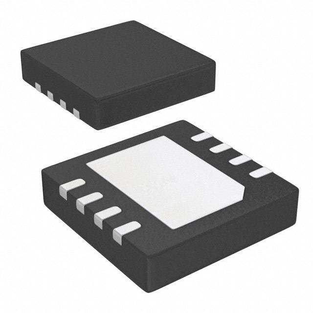
| 供应商器件封装 | 24-VQFN |
| 其它名称 | MSL3080IU |
| 内部驱动器 | 是 |
| 包装 | 托盘 |
| 安装类型 | 表面贴装 |
| 封装/外壳 | 24-VFQFN 裸露焊盘 |
| 工作温度 | -40°C ~ 85°C |
| 恒压 | - |
| 恒流 | - |
| 拓扑 | 回扫,开路漏极,PWM,Sepic,升压(升压) |
| 标准包装 | 2,450 |
| 特色产品 | http://www.digikey.cn/product-highlights/cn/zh/atmel-led-drivers/2994 |
| 电压-电源 | 4.5 V ~ 5.5 V |
| 电压-输出 | 40V |
| 类型-初级 | 通用 |
| 类型-次级 | 白色 LED |
| 输出数 | 8 |
| 频率 | 16MHz ~ 24MHz |


- 商务部:美国ITC正式对集成电路等产品启动337调查
- 曝三星4nm工艺存在良率问题 高通将骁龙8 Gen1或转产台积电
- 太阳诱电将投资9.5亿元在常州建新厂生产MLCC 预计2023年完工
- 英特尔发布欧洲新工厂建设计划 深化IDM 2.0 战略
- 台积电先进制程称霸业界 有大客户加持明年业绩稳了
- 达到5530亿美元!SIA预计今年全球半导体销售额将创下新高
- 英特尔拟将自动驾驶子公司Mobileye上市 估值或超500亿美元
- 三星加码芯片和SET,合并消费电子和移动部门,撤换高东真等 CEO
- 三星电子宣布重大人事变动 还合并消费电子和移动部门
- 海关总署:前11个月进口集成电路产品价值2.52万亿元 增长14.8%


PDF Datasheet 数据手册内容提取
MSL3050/MSL3060/MSL3080 Datasheet Preliminary 5, 6 and 8 String 60mA LED Drivers with Integrated Boost Controller ____________________ Key Features ______________ General Description Drives 5/6/8 parallel 60mA LED strings at up to 40V LED The MSL3050/MSL3060/MSL3080 multi-channel LED drivers with string voltage integrated boost regulator controller offer a complete solution to Integrated boost controller drive parallel LED strings at up to 40V. The LED current sinks Offers true 12-bit LED dimming at 200Hz control up to 60mA each for up to 19W of LED power. The String open Acircuitt amnd LEeD shlo rt McircuiSt faulLt det3ecti0on a8nd 0 MSL3050 has five current sinks, the MSL3060 has six and the automatic shut down MSL3080 has eight. Parallel connect the current sinks for ±3% current accuracy and current balance increased string current. A single resistor sets LED current, with Single resistor sets current for all LED strings s tring matching and accuracy within ±3%. EInxteternr8naal lP SPWWtMMr d idimnimmmgining g 6c o0ntrmol enAgin eL ED Drivers Tdihmem aidnvga, nacnedd o ifnfetergs rsaitmedp lPe WPWM Mci rdciumitmryi nagll ocwosn turopl .t oE x4t0e9rn5a:1l PWM wi thSInitn egIrnlnea Plt PWeWMgM in drpimuat msteientsg d d(uims eBm oinpogti odonuatysl) ctyc lCe anod nfretqureoncly l er dimming is controlled by a signal at the PWM input, which sets Synchronizes PWM dimming to LCD panel refresh rate bTohteh itnhtee rPnaWl MPW duMty d cimycmlein agn ids fcroenqturoelnlecdy boyf trheeg idsitmerms iancgc seisgsniabllse. Frequency multiplier allows PWM dimming at multiples of t hrough the I2C serial interface. L1CMDH zp aI²nCe/Sl rMefBreussh i nfrteeqrfFuaecneUc; yu Ls(see Loep PtiDorongaArla mTmAingS GuHideE) ET The MSL3050/60/80 feature integrated fault detection circuitry Resistor programmable LED short circuit threshold that detects and acts upon string open-circuit and LED short Die over-temperature cut-off protection circuit faults, boost regulator over-voltage faults, and die over- -40°C to +85°C operating temperature range Features: temperature faults. A proprietary Efficiency Optimizer maintains Lead free, halogen free, RoHS compliant package sufficient boost regulator output voltage to maintain LED current regulation while minimizing power use. A 1MHz I2C/SMBus serial _______________ Application Circuit • Drives 8 paralleinl te6rf0acme aAllo LwsE oDptio snatlr dinimgmsin ga cto nutropl, ftaoul t inspection and 40V LED string cvonotrlotla ogf deriver configuration; for serial interface information see VIN= 5V VPWR= 12V the MSL3050/60/80/50/60/80/86/87/88 Programming Guide. • Integrated boos t controller 10H10F • Offers true 12-bTiht eL MESLD30 5d0i/m60/m80 ianreg o fafetre 1d i2n 0thHe 2z4-pin VQFN lead-free, 60V 3A 20F halogen-free, RoHS compliant package and operate over -40°C VIN PVIN • String open circtuo +it8 5a°Cn. d LED short circuit fault detection GACTSE F56D1C2 VLED and automatic s _h_u_t _d_o_w_n______________ Applications ENABLE EN 25m 47.5k • ±3% current accuracy and current balance MSL3080 FB • Single resistor sL eontgs L icfeuT, eErlferfievciiseninottn Lsf EoaDnrd B aDalcelks lkLigtohEpti nDMgo fnosirtt:o rrisn gs INTEIR2CF ACE SDA COMP2nF22k 3.12k • External PWM d immiMnegdical and Industrial Instrumentation SCL Automotive Audio-Visual Displays • Internal PWM dCAimrhcahnmitneecilnt uSrgiagl n Lcsi gohntintgr ol engine OFUATUPLUTT FLTB • Single PWM input sets dimming duty cycle and frequency • Internal PWM d i_m_m__in_g_ _(_u_se__ o_p_t ioOnradl)ering Information INPWPUMT PWM SSTTRR10 • Synchronizes PWPMAR Td imming tDoE SLCCRDIPT pIOaNnel refresh PrKaGte ILED SSTTRR32 •• Fo1fMr eLHqCuzDe I np²cCayn/ SmeMlu rleBtifpurMelsiSes Lirh3n 0 a5tf0erl leorqf5cCPwao-WiuCrncscHtMeur oe i tLPnil nltEe;hpcrWD ru euay tds.n hsrMdi(ov erseled res d swioseeiitttmohpt irn P itbngmiat,er oswgoieinrntdahg t gaLesrEdi anlD agbm loSeto hsmmot rt uinltg4i p xG l4eV2 xu4Qs 0ipF .di7Nn5e m)m 91.3k FBPIGND GND ESSSPSTTTTRRRR4567 •• RDeies iosvtoerr -pteromgpraemrMaSmtLu30ar6e0b lce6cCPuo-W iCrnLctHtMur-Eo i otLil nltEehDpfrDrfu ea t ds.np shrdiov rhreleodros swtiseeritttohtticrn icbngtat,ie isworgeicrtdnah ut LesEdiinD tgb loSetoh hsotr rte s4h xo 4V2l xd4Q 0pF.i7Nn5 mm APPLICATION CIRCUIT •• -L4e0a°dC f rteoe +, 8h5a°lCog MoeSpnL3e 0fr8r0ae tei8cCPno-,WiCrn gcHtMRur o i tLitl onltEeehprDrHu mea tds.n Shrdipov rel edercs swiroseiatttohtmirn t ibnguat,pe rswgeleiritdaha t LesrnEdianD gtbn loSepo ghsoate rtc k4a xg 4V2e x4Q 0pF.i7Nn5 mm I²C and SMBus are trademarks of their respective owners. MSL3050/60/80 preliminary datasheet revision 0.1 Page 1 of 24 © Atmel Inc., 2011. All rights reserved. Description: The MSL3080 8-channel LED drivers with integrated boost regulator controller offers a complete solution to drive parallel LED strings at up to 40V. The LED current sinks control up to 60mA each for up to 19W of LED power. The MSL3080 has eight current sinks. Parallel connect the current sinks for increased string current. A single resistor sets LED current, with string matching and accuracy within ±3%. The advanced integrated PWM circuitry allows up to 4095:1 dimming, and offers simple PWM dimming control. External PWM dimming is controlled by a signal at the PWM input, which sets both the PWM duty cycle and frequency of the dimming signals. The internal PWM dimming is controlled by registers accessible through the I2C serial interface. The MSL3080 feature integrated fault detection circuitry that detects and acts upon string open-circuit and LED short circuit faults, boost regulator over-voltage faults, and die over-temperature faults. A proprietary Efficiency Optimizer maintains sufficient boost regulator output voltage to maintain LED current regulation while minimizing power use. A 1MHz I2C/SMBus serial interface allows optional dimming control, fault inspection and control of driver configuration; for serial interface information see the “MSL3040/50/60/80/86/87/88 Programming Guide”. The MSL3080 IS offered in the 24-pin VQFN lead-free, halogen-free, RoHS compliant package and operate over -40°C to +85°C. Atmel MSL3080 Datasheet 1 8 String 60mA LED Driver with Integrated Boost Controller DBIE-20120814
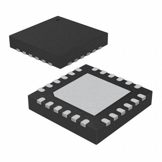
Table of Contents 1.0 Packages and Pin Connections .................................................................3 2.0 Pin Descriptions ..........................................................................................4 3.0 Absolute Maximum Ratings .......................................................................5 4.0 Electrical Characteristics ...........................................................................6 5.0 Typical Operating Characteristics .............................................................7 6.0 Block Diagram .............................................................................................9 7.0 Typical Application Circuits .....................................................................10 8.0 Detailed Description .................................................................................13 8.1 LED Driver Comparison .................................................................................................13 8.2 Boost Regulator Overview .............................................................................................14 8.3 Error Amplifier ................................................................................................................14 8.4 Gate Driver ....................................................................................................................15 8.5 Soft-Start .......................................................................................................................15 8.6 Boost Fault Monitoring and Protection ..........................................................................15 8.7 LED Current Regulators and PWM Dimming Modes ....................................................15 8.8 Efficiency Optimizer (EO) ..............................................................................................15 8.9 Fault Monitoring and Auto-Handling ..............................................................................15 8.10 Internal Supervisory and LDO .......................................................................................16 8.11 Internal Oscillator ...........................................................................................................16 8.12 Over Temperature Shutdown .........................................................................................16 8.13 Power Saving Modes .....................................................................................................16 8.14 I2C Serial Interface and Driver Control...........................................................................16 9.0 Application Information ............................................................................17 9.1 Bypassing VIN and PVIN ...............................................................................................17 9.2 Setting the LED Current ................................................................................................17 9.3 Fault Monitoring and Automatic Fault Handling .............................................................17 9.4 Setting the LED Short-Circuit Threshold ........................................................................17 9.5 Boost Regulator .............................................................................................................18 9.6 The Efficiency Optimizer (EO) .......................................................................................19 9.7 Setting the Boost Regulator Output Voltage ..................................................................20 9.8 Choosing the Input and output Capacitors ....................................................................20 9.9 Choosing the Inductor ...................................................................................................20 9.10 Setting the External MOSFET Current Limit ..................................................................21 9.11 Choosing the Switching MOSFET .................................................................................21 9.12 Choosing the Output Rectifier .......................................................................................21 9.13 Loop Compensation ......................................................................................................21 10.0 LED Dimming Control ...............................................................................23 11.0 Ordering Information ................................................................................23 Atmel MSL3080 Datasheet 2 8 String 60mA LED Driver with Integrated Boost Controller
PHASE SHIFTED LEDDIMMING SIGNALS By default, string PWM dimming is staggered in time to reduce the transient current demand on the boost regulator. The MSL3050/MSL3060/MSL3080 Datasheet 1.0 Packages and Pin Connections MSL3040/41 automatically determine the stagger times based on the number of enabled strings and the PWM dimming Preliminary frequency. Package Pin Description 1.1 24 pin 4 x 4 x 0.75mm VQFN PacPkaHgAeSE SHIFT ED LEDDIMMING SIGNALS By default, strinPg aPcWkMa dgimem inIng ifso srtamggearteido inn ti me to reduce the transient current demand on the boost regulator. The MSL3040/41 automatically determine the stagger times based on the number of enabled strings and the PWM dimming GND COMP CS EN FLTB PVIN GND COMP CS EN FLTB PVIN f requency. 24 23 22 21 20 19 24 23 22 21 20 19 ● ● Package Information FB 1 18 GATE FB 1 18 GATE VIN 2 17 PGND VIN 2 17 PGND SDA 3 PHASE 1S6HILEIDF TED LEDSDDA I3M MING SIGNALS 16 ILED MSL3050 MSL3080 SCL 4 (TOP VIEWB) y defa u1l5t,C sGNtDri ng PWM SdCLim4 m ing is s(TtOaPg VgIEeWr)e d in ti m15e CtGoN Dr educe the transient current demand on the boost regulator. The MSL30 40 /4 1 automatically de termine the stagger tim es based on the number of enabled strings and the PWM dimming SCTH 5 14 PWM SCTH 5 14 PWM frequen cy . STR0 6 13 CGND STR0 6 13 STR7 7 8 9 10 11 12 7 8 9 10 11 12 Package Information STR1 STR2 STR3 PByHSTR4 dAe SfEaCGND u Slt,H sI FtCGND rTinEgD P L WEMD dDimIMmMinIgN iGs sStIaGgNgAerLeSd in ti meSTR1 to reSTR2 du ce STR3 the trSTR4 ans ienSTR5 t curSTR6 rent de mand on the boost regulator. The MSL3040/41 automatically determine the stagger times based on the number of enabled strings and the PWM dimming frequency. Package Information GND COMP CS EN FLTB PVIN 24 23 22 21 20 19 ● FB 1 18 GATE VIN 2 17 PGND SDA 3 16 ILED MSL3060 SCL 4 (TOP VIEW) 15 CGND SCTH 5 14 PWM STR0 6 13 CGND 7 8 9 10 11 12 STR1 STR2 STR3 STR4 STR5 CGND MSL3050/60/80 preliminary datasheet revision 0.1 Page 2 of 24 © Atmel Inc., 2011. All rights reserved. Atmel MSL3080 Datasheet Page 22 of 22 3 © Atmel Inc., 2011. All rights reserved. 8 String 60mA LED Driver with Integrated Boost Controller Page 22 of 22 © Atmel Inc., 201 1. All rights reserved. Page 22 of 22 © Atmel Inc., 2011. All rights reserved. Page 22 of 22 © Atmel Inc., 2011. All rights reserved.
2.0 Pin Descriptions Table 2.1 Pin Assignments Name MSL3080 Pin Description FB 1 VLED Voltage Regulator Feedback Input: Connect a resistive voltage divider from the boost regulator output, VLED, to FB to set the un- optimized boost regulator output voltage. The feedback regulation voltage is 2.5V. VIN 2 Power Supply Input: Power supply input. Apply 4.5V to 5.5V to VIN. Decouple VIN to GND a 1µF or greater capacitor placed close to VIN. I²C Serial Data I/O: SDA is the I²C serial interface data input/output. Connect SDA to VIN when unused. For interface information see the SDA 3 “MSL3040/50/60/80/86/87/88 Programming Guide”. I²C Serial Clock Input: SCL is the I²C serial interface clock input. Connect SCL to VIN when unused. For interface information see the SCL 4 “MSL3040/50/60/80/86/87/88 Programming Guide”. String Short Circuit Threshold Level Setting Input: SCTH programs the LED string short-circuit detection threshold. Connect a resistor from SCTH to GND to set the short-circuit threshold level to 4.9V (1kΩ), 5.8V (27kΩ), 6.8V (68kΩ) or 7.6V (330kΩ). A short circuit is detected SCTH 5 when the STRn voltage is above the threshold while STRn is on. See the section “Setting the LED Short-Circuit Threshold” on page 17 for information. STR0 6 LED String 0 Current Sink: Connect the cathode end of series LED String 0 to STR0. If not used, connect STR0 to GND. STR1 7 LED String 1 Current Sink: Connect the cathode end of series LED String 1 to STR1. If not used, connect STR1 to GND. STR2 8 LED String 2 Current Sink: Connect the cathode end of series LED String 2 to STR2. If not used, connect STR2 to GND. STR3 9 LED String 3 Current Sink: Connect the cathode end of series LED String 3 to STR3. If not used, connect STR3 to GND. STR4 10 LED String 4 Current Sink: Connect the cathode end of series LED String 4 to STR4. If not used, connect STR4 to GND. STR5 11 LED String 5 Current Sink: Connect the cathode end of series LED String 5 to STR5. If not used, connect STR5 to GND. STR6 12 LED String 6 Current Sink: Connect the cathode end of series LED String 6 to STR6. If not used, connect STR6 to GND. STR7 13 LED String 7 Current Sink: Connect the cathode end of series LED String 7 to STR7. If not used, connect STR7 to GND. CGND 15 Connect To Ground: Connect CGND to GND close to the driver. PWM Dimming and Synchronization Input: Drive PWM with a pulse-width modulated signal with duty cycle of 0% to 100% and frequency of PWM 14 20Hz to 50kHz to control the duty cycle and the frequency of all LED strings. For serial interface controlled PWM dimming connect PWM to GND and refer to the register definitions section for registers 0x10 through 0x14 in the “MSL3040/50/60/80/86/87/88 Programming Guide”. Maximum LED Current Control Input: Connect a resistor from ILED to GND to set the full-scale LED current. See the section “Setting the ILED 16 LED Current” on page 17 for more information. PGND 17 Power Ground: Ground of the boost regulator gate driver. Connect PGND to GND, EP and CGND as close to the MSL3080 as possible. GATE 18 Gate Drive Output: Connect GATE to the gate of the boost regulator switching MOSFET Boost Regulator Power Supply Input: PVIN is the power supply input for the external MOSFET gate driver. Apply 4.5V to 5.5V to PVIN. PVIN 19 Decouple PVIN with two 1µF capacitors placed close to PVIN. Fault Output: FLTB sinks current to GND when a fault is detected. Clear faults by toggling EN low and then high, by cycling input power off FLTB 20 and on, or through the I2C serial interface; see the “MSL3040/50/60/80/86/87/88 Programming Guide” for information. Enable Input: Drive EN high to turn on the device, drive it low to turn it off. For automatic startup connect EN to VIN. Toggle EN low then high EN 21 to reset FLTB, or reset it through the I2C serial interface. Boost Regulator Current Sense Input: Connect the current sense resistor from CS and the MOSFET source to GND to set the boost regulator CS 22 current limit. The current limit threshold is 100mV. See the section “Setting the External MOSFET Current Limit” beginning on page 21 for more Boost Regulator Compensation Node: Connect the compensation network components from COMP to FB to compensate the boost regulator COMP 23 control loop, as shown in the Typical Applications Circuit on page 10. See the section “Loop Compensation” beginning on page 21 for more information. GND 24 Signal Ground: Connect GND to EP, PGND and CGND as close to the device as possible. Exposed Die-Attach Paddle: Connect EP to GND, CGND, PGND and to the system ground. EP is the return path for the LED current as well as the primary thermal path to remove heat generated in the MSL3080. Use a large circuit board trace to connect from EP to the boost supply EP EP output capacitor ground and to the input supply ground return. Connect EP to a large copper ground plane for best thermal and electrical performance. Atmel MSL3080 Datasheet 4 8 String 60mA LED Driver with Integrated Boost Controller
3.0 Absolute Maximum Ratings Voltage (with respect to GND) VIN, PVIN, EN, SDA, SCL, PWM, FLTB, SCTH, ILED, CS, COMP, FB, GATE ............................................................... -0.3V to +5.5V STR0 to STR7 ................................................................................................................................................................... -0.3V to +40V PVIN to VIN ....................................................................................................................................................................................... ±1V PGND, CGND, EP ...........................................................................................................................................................-50mV to 50mV Current (into pin) VIN .................................................................................................................................................................................................50mA GATE, PVIN ...............................................................................................................................................................................±1250mA STR0 to STR7, CGND .....................................................................................................................................................................75mA EP, PGND, GND .........................................................................................................................................................................-1000mA All other pins .....................................................................................................................................................................-20mA to 20mA Continuous Power Dissipation 24-Pin 4mm x 4mm VQFN (derate 25mW/°C above TA = +70°C) ..............................................................................................1850mW Ambient Operating Temperature Range TA = TMIN to TMAX .......................................................................................................... -40°C to +85°C Junction to Ambient Thermal Resistance (θJA), 4-Layer (Note 8) ............................................................................................................29°C/W Junction to Ambient Thermal Resistance (θJA), 2-Layer (Note 8) ............................................................................................................38°C/W Junction to Case Thermal Resistance (θJC) ............................................................................................................................................8.6°C/W Junction Temperature ............................................................................................................................................................................. +125°C Storage Temperature Range ..................................................................................................................................................... -65°C to +125°C Lead Soldering Temperature, 10s ............................................................................................................................................................+300°C Atmel MSL3080 Datasheet 5 8 String 60mA LED Driver with Integrated Boost Controller
4.0 Electrical Characteristics VVIN = 5V, VEN = 5V, Default Register Settings of Table 1, TA = -40°C to 85°C, unless otherwise noted. Typical values are at TA = +25°C Parameter Conditions and Notes Min Typ Max Unit DC Electrical Characteristics VIN Operating Supply Voltage 4.5 5.5 V VIN Operating Supply Current All STRn outputs 100% duty 18 mA VIN Shutdown Supply Current EN = GND 1 µA SDA, SCL, PWM, SYNC Input High Voltage 1.82 V SDA, SCL, PWM, SYNC Input Low Voltage 0.72 V Minimum PWM On-Time 400 ns PWM, SYNC Input Frequency Range 20 200 50,000 Hz SDA, FLTB Output Low Voltage Sinking 6mA 0.4 V EN Threshold VEN rising 1.5 V ILED Regulation Voltage Minimum RILED = 60kΩ 1.25 V STR0 to STR7 LED Regulation Current RILED = 100kΩ, TA= 25°C VSTRn = 1V 58.2 60.0 61.8 mA STR0 to STR7 LED Current Load Regulation RILED = 100kΩ VSTRn = 1V to 5V 0.15 %/V STR0 to STR7 LED Current Matching String to average of all strings -3 3 % STR0 to STR7 Minimum Headroom VSTRn = 60mA 0.5 V STR0 to STR7 Short Circuit Fault Threshold RSCTH = 1.0kΩ 3.98 4.96 V FB Feedback Output Current FBO DAC = 0xFF, VFB = 0 224 350 µA FB Feedback Output Current Step Size 1.1 µA FBI Input Disable Threshold 50 mV Thermal shutdown temperature Temperature Rising, 10°C Hysteresis 135 °C Boost Regulator Electrical Characteristics Switching Frequency 569 665 762 kHz Gate Voltage Rise/Fall Time CGATE = 1nF 50 ns CS Current Limit Threshold Voltage 75 111 147 mV Maximum Duty Cycle At factory set boost frequency 90.1 % Minimum On Time fBOOST = 350kHz to 1MHz (contact factory for boost frequencies different 241 300 ns from 625kHz) Boost Regulator Leading-Edge Blanking Period 130 ns FB Regulation Voltage 2.4 2.5 2.6 V I²C Switching Characteristics SCL Clock Frequency 1/tSCL Bus timeout disabled (Note 1) 0 1000 kHz Bus Timeout Period ttimeout TA = 25°C (Note 7) 29 30 ms STOP to START Condition Bus Free Time tBUF (Note 7) 0.5 µs Repeated START condition Hold Time tHD:STA (Note 7) 0.26 µs Repeated START condition Setup Time tSU:STA (Note 7) 0.26 µs STOP Condition Setup Time tSU:STOP (Note 7) 0.26 µs SDA Data Hold Time tHD:DAT (Note 7) 0 ns SDA Data Valid Acknowledge Time tVD:ACK (Note 2) (Note 7) 0.05 0.55 µs SDA Data Valid Time tVD:DAT (Note 3) (Note 7) 0.05 0.55 µs SDA Data Set-Up Time tSU:DAT (Note 7) 100 ns SCL Clock Low Period tLOW (Note 7) 0.5 µs SCL Clock High Period tHIGH (Note 7) 0.26 µs SDA, SCL Fall Time tf (Note 4) (Note 5) (Note 7) 120 ns SDA, SCL Rise Time tr (Note 7) 120 ns SDA, SCL Input Suppression Filter Period tSP (Note 6) (Note 7) 50 ns Note 1. Minimum SCL clock frequency is limited by the bus timeout feature, which resets the serial bus interface if either SDA or SCL is held low for timeout. Note 2. tVD:ACK = SCL LOW to SDA (out) LOW acknowledge time. Note 3. tVD:DAT = minimum SDA output data-valid time following SCL LOW transition. Note 4. A master device must internally provide an SDA hold time of at least 300ns to ensure an SCL low state. Note 5. The maximum SDA and SCL rise times is 300ns. The maximum SDA fall time is 250ns. This allows series protection resistors to be connected between SDA and SCL inputs and the SDA/SCL bus lines without exceeding the maximum allowable rise time. Note 6. MSL3080 include input filters on SDA and SCL that suppress input noise less than 50ns Note 7. Parameter is guaranteed by design and not production tested. Note 8. Per JEDEC specification JESD51-5 and JESD51-12. Note 9. Tests performed at TA = 25°C, specifications over temperature guaranteed by design. Atmel MSL3080 Datasheet 6 8 String 60mA LED Driver with Integrated Boost Controller
MSL3050/MSL3060/MSL3080 Datasheet Preliminary 5.0 Typical Operating Characteristics Typical Operating Characteristics (Typical Operating Circuit, unless otherwise stated) (Typica l Operating Circuit, unless otherwise stated, TA = +25°C, unless otherwise noted) BOOST REGULATOR EFFICIENCY vs. SUSPUPPLPYL CYU CRURRERNETN T OUTPUT CURRENT vsv. sS.U SPUPPLPYL VYO VLOTALTGAEGE 100 110000000000 EN = 1 EN = 1 95 100000 sleep = slpPwrSv = 1 sleep = slpPwrSv = 0 90 1000 BOOST NOT SWITCHING 10000 %) 85 100 EN = 1 Y ( 80 1000 sleep = slpPwrSv = 0 EFFICIENC 7705 I (µA)I(µA)ININ 11011000 EslNee =p 1= slpPwrSv =B 1OOST NOT SWITCHING 65 VPWR = 12V 1 EN = 0EN = 0 60 VLED 37V 0.1 55 fBOOST = 625kHz 0.1 50 0.010.01 0 200 400 600 800 1,000 4.54.45.6 44.6.7 44.7.8 44..89 45..90 55..10 55..21 55.3.2 55.4.3 5.55.4 5.5 OUTPUT CURRENT (mA) VIN (VV)IN(V) STRn CURRENT vs. RISET START-UP WAVEFORMS 75 70 65 60 A55 m50 NT (45 RE40 UR35 n C30 R25 T S20 15 10 5 0 10 100 1000 RISET (k)MSL3050/MSL3060/MSL3080 Datasheet CH1 = V , CH2 = V , CH3 = V , CH4 = I EN LED STRx PPWreRliminary START-UP WAVEFORMS (ZOOM) BOOST WAVEFORMS 10% LED DUTY CYCLE MSL3050/60/80 preliminary datasheet revision 0.1 Page 6 of 24 © Atmel Inc., 2011. All rights reserved. CH1 = VEN, CH2 = VLED, CH3 = VSTRx, CH4 = IPWR CH1 = V , CH2 = V , CH3 = I LED GATE INDUCTOR AUTO CALIBRATION BOOST WAVEFORMS 100% LED DUTY CYCLE Atmel MSL3080 Datasheet 7 8 String 60mA LED Driver with Integrated Boost Controller CH2 = VLED, CH3 = VSTRx CH1 = V , CH2 = V , CH3 = I LED GATE INDUCTOR MSL3050/60/80 preliminary datasheet revision 0.1 Page 7 of 24 © Atmel Inc., 2011. All rights reserved.
MSL3050/MSL3060/MSL3080 Datasheet Preliminary START-UP WAVEFORMS (ZOOM) BOOST WAVEFORMS 10% LED DUTY CYCLE 5.0 TypCicH1a =l VOENp, eCHra2 t=i nVLgED ,C CHh3a =r aVScTRtxe, rCiHs4t i=c IPsW R(continued) CH1 = VLED, CH2 = VGATE, CH3 = IINDUCTOR (Typic al Operating Circuit, unless otherwise stated, TA = +25°C, unless otherwise noted) AUTO CALIBRATION BOOST WAVEFORMS 100% LED DUTY CYCLE MSL3050/M SL3060/MSL3080 Datasheet CH2 = VLED, CH3 = VSTRx C H1 = VLED, CH2 = VGATE, CH3 = IINDUCTOR Preliminary BOOST REGULATOR WAVEFORMS BOOST REGULATOR GATE DRIVE RISE/FALL 10% TO 99.5% LED DUTY CYCLE WITH 3nF CAPACITIVE LOAD MSL3050/60/80 preliminary datasheet revision 0.1 Page 7 of 24 © Atmel Inc., 2011. All rights reserved. CH1 = V , CH2 = V , CH3 = V , CH4 = I CH2 = V LED GATE PWM INDUCTOR GATE DRIVER RISE TIME DRIVER FALL TIME AUTOMATIC PHASE SHIFTED PWM DIMMING This scope image shows the voltage (VSTR0) and current (ISTR0) This scope image shows the voltage (VSTR0) and current (ISTR0) waveforms for string zero, and their turn-on rise times and delay waveforms for string zero, and their turn-off fall times. Also shown from PWM rising. Also shown is the string power supply output is the string power supply output (VLED), which shows very little C(HV1LE =D )V, SwThRi0c,h CshHo2w s= l iVttlSeT dRi2s,t uCrbHa3nc =e. VFSoTr Rth4,is C pHho4to = s tVrinSgTR 06 is disturbance. For this photo string 0 is enabled with all other strings enabled with all other strings disabled. disabled, and a 220pF capacitor in series with a 11Ω resistor in series is placed from STR0 to GND at the device. Atmel MSL3080 Datasheet 8 8 String 60mA LED Driver with Integrated Boost Controller MSL3050/60/80 preliminary datasheet revision 0.1 Page 8 of 24 © Atmel Inc., 2011. All rights reserved.
MSL3050/MSL3060/MSL3080 Datasheet Preliminary 6.0 BBlloocckk D Diaigargarmam Figure 6.1. Block Diagram MSL3080 Figure 1. MSL3050/MSL3060/MSL3080 Block Diagram MSL3050/60/80 preliminary datasheet revision 0.1 Page 9 of 24 © Atmel Inc., 2011. All rights reserved. Atmel MSL3080 Datasheet 9 8 String 60mA LED Driver with Integrated Boost Controller
MSL3050/MSL3060/MSL3080 Datasheet Preliminary 7.0 Typical Application Circuits Figure 7.1. Typical Operating Circuit for Eight 60mA Strings of 10 White LEDs each. Typical Application Circuits VPWR = 12V 10 F VIN= 5V 10 H 1 F 2x 1 F 2x B380 10 F 2 19 VIN PVIN 18 GATE FDC5612 CS 22 VLED 21 ENABLE EN 25m 47.5k 3 I2C SDA 1 INTERFACE 4 MSL3080 FB SCL 22k 3.12k PWM 14 PWM INPUT 2nF FAULT 20 23 FLTB COMP OUTPUT 5 SCTH 82k 6 STR0 7 16 STR1 ILED 8 STR2 9 STR3 93.1k 10 STR4 11 STR5 15 12 CGND STR6 13 STR7 PGND EP GND 17 24 Figure 2. Typical Operating Circuit for Eight 60mA Strings of 10 White LEDs each. MSL3050/60/80 preliminary datasheet revision 0.1 Page 10 of 24 © Atmel Inc., 2011. All rights reserved. Atmel MSL3080 Datasheet 10 8 String 60mA LED Driver with Integrated Boost Controller
MSL3050/MSL3060/MSL3080 Datasheet Figure 7.2. Typical Operating Circuit for Four 120mA Strings of 10 White LEDs each. Preliminary VPWR = 12V 10 F VIN= 5V 10 H 1 F 2x 1 F 2x B380 10 F 2 19 VIN PVIN 18 GATE FDC5612 CS 22 VLED 21 ENABLE EN 25m 47.5k 3 I2C SDA 1 INTERFACE 4 MSL3080 FB SCL 22k 3.12k PWM 14 PWM INPUT 2nF FAULT 20 23 FLTB COMP OUTPUT 5 SCTH 82k 6 STR0 7 16 STR1 ILED 8 STR2 9 STR3 93.1k 10 STR4 11 STR5 15 12 CGND STR6 13 STR7 PGND EP GND 17 24 Figure 3. Typical Operating Circuit for Four 120mA Strings of 10 White LEDs each. MSL3050/60/80 preliminary datasheet revision 0.1 Page 11 of 24 Atmel MSL3080 Datasheet 11 8 String 60mA LED Driver with Integrated Boost Controller © Atmel Inc., 2011. All rights reserved.
MSL3050/MSL3060/MSL3080 Datasheet Figure 7.3. Typical Operating Circuit for One 480mA String of 10 White LEDs. Preliminary VPWR = 12V 10 F VIN= 5V 10 H 1 F 2x 1 F 2x B380 10 F 2 19 VIN PVIN 18 GATE FDC5612 CS 22 VLED 21 ENABLE EN 25m 47.5k 3 I2C SDA 1 INTERFACE 4 MSL3080 FB SCL 22k 3.12k PWM 14 PWM INPUT 2nF FAULT 20 23 FLTB COMP OUTPUT 5 SCTH 82k 6 STR0 7 16 STR1 ILED 8 STR2 9 STR3 93.1k 10 STR4 11 STR5 15 12 CGND STR6 13 STR7 PGND EP GND 17 24 Figure 4. Typical Operating Circuit for One 480mA String of 10 White LEDs. Detailed Description The MSL3050/MSL3060/MSL3080 are LED drivers with five, six and eight internal current regulators respectively, each capable of driving up to 60mA LED current They feature an integrated boost regulator controller with a proprietary Efficiency Optimizer voltage control algorithm that lowers power use to the minimum required to assure LED current regulation. The driver outputs allow parallel connection to increase string current, at the expense of the number of strings, and a single resistor sets the current for all strings. The drivers support 12-bit PWM LED dimming ratios. The driver synchronizes LED dimming and controls duty cycle with a single external digital signal at the PWM input. The MSL3050/60/80 include comprehensive fault monitoring and automatic fault handling. Automatic fault handling allows the drivers to operate without any microcontroller or FPGA, while optional control via I2C allows customized fault handling and driver control for more complex applications. All drivers also feature optional register-set PWM dimming, fault management and other controls via the I2C serial interface; for interface information see the MSL3050/60/80/50/60/80/86/87/88 Programming Guide. The small 4x4mm VQFN package allows a small overall LED driver solution, while maintaining high package power dissipation for high output power capability. Atmel MSL3080 Datasheet 12 MSL3050/60/80 preliminary datasheet revision 0.1 Page 12 of 24 8 String 60mA LED Driver with Integrated Boost Controller © Atmel Inc., 2011. All rights reserved.
8.0 Detailed Description The MSL3080 is an LED driver with eight internal current regulators, each capable of driving up to 60mA LED current. They feature an integrated boost regulator controller with a proprietary Efficiency Optimizer voltage control algorithm that lowers power use to the minimum required to assure LED current regulation. The driver outputs allow parallel connection to increase string current, at the expense of the number of strings, and a single resistor sets the current for all strings. The drivers support 12-bit PWM LED dimming ratios. The driver synchronizes LED dimming and controls duty cycle with a single external digital signal at the PWM input. The MSL3080 includes comprehensive fault monitoring and automatic fault handling. Automatic fault handling allows the drivers to operate without any microcontroller or FPGA, while optional control via I2C allows customized fault handling and driver control for more complex applications. All drivers also feature optional register-set PWM dimming, fault management and other controls via the I2C serial interface; for interface information see the “MSL3040/50/60/80/86/87/88 Programming Guide”. The small 4x4mm VQFN package allows a small overall LED driver solution, while maintaining high package power dissipation for high output power capability 8.1 LED Driver Comparison Table 8.1. LED Driver Comparison with Similar Parts MAX PHASE RESISTOR SET NUMBER CURRENT SHIFTED INTERNAL LED SHORT SEPARATE OF LED PER STRING BOOST CIRCUIT SYNC PART STRINGS STRING DRIVERS CONTROLLER THRESHOLD INPUT*** BEST FOR MSL3086 8 60mA YES YES YES NO MONITOR, INDUSTRIAL PANEL MSL3087* 8 60mA YES NO YES NO SMALL TV MSL3088 8 60mA YES YES NO YES SMALL TV 8 60mA NO YES YES NO MONITOR, INDUSTRIAL PANEL 4** 120mA NO YES YES NO MONITOR, INDUSTRIAL PANEL MSL3080 2** 240mA NO YES YES NO MONITOR, INDUSTRIAL PANEL 1** 480mA NO YES YES NO MONITOR, INDUSTRIAL PANEL MSL3040* 4 120mA YES YES YES NO MONITOR, AUTOMOTIVE MSL3041* 4 120mA YES YES YES YES MONITOR, AUTOMOTIVE 5 60mA NO YES YES NO INDUSTRIAL PANEL MSL3050* 1** 300mA NO YES YES NO INDUSTRIAL PANEL 6 60mA NO YES YES NO MONITOR, INDUSTRIAL PANEL 3** 120mA NO YES YES NO MONITOR, INDUSTRIAL PANEL MSL3060* 2** 180mA NO YES YES NO MONITOR, INDUSTRIAL PANEL 1** 360mA NO YES YES NO MONITOR, INDUSTRIAL PANEL * Future product, contact factory for information. ** Drivers without phase shift allow parallel connection of string drive outputs for increased string current. *** Drivers with separate SYNC input expect two control signals, one for dimming duty cycle and one for dimming frequency. Atmel MSL3080 Datasheet 13 8 String 60mA LED Driver with Integrated Boost Controller
8.2 Boost Regulator Overview The MSL3080 boost regulator boosts the input voltage up to the regulated output voltage (for design details see the section “Boost Regulator” beginning on page 17, the following text presents an overview of the boost regulator controller). The boost regulator uses an external switching MOSFET, current sense resistor, inductor, rectifier, and input and output capacitors (Figure 8.1). External MOSFET and current sense resistor allow the boost regulator to operate over wide input and output voltage ranges, and LED currents. It includes a 2.5V reference voltage, fixed slope compensation and external voltage regulator compensation to optimize the control loop for each configuration. Because the boost regulator components are external it supports a number of converter topologies, such as SEPIC, flyback, and single-switch forward. The boMost SregLula3tor0 inc5lud0es/ sMoft-sStarLt, a3dju0sta6ble0 cy/cMle-bSy-cyLcle3 cu0rre8nt 0lim itiDng,a antd aoutspuht oveer-et volt age fault detection. Preliminary Figu re 8.1. Power Section of MSL3080 5V VPWR CIN PVIN L1 D1 VLED GATE DRIVE GATE LIMIT CS Q1 COUT CURRENT 0.1 V RCS RESR 1.1V GND A = 11 SENSE RTOP SLOPE COMP EFFICIENCY FB 0.4V + OPTIMIZER 1.5V SOFT RCOMP CCOMP2 START CCOMP1 RBOTTOM COMP REF COMPENSATION: CCOMP2= POLE CCOMP1, RCOMP= ZERO DROPOUT DETECT STRn MSL3080 MSL3050 LED MSL3060 CURRENT MSL3080 SINK Figure 5. Power section of MSL3050/60/80 8.3 ErrorE ARmROpRli fiAeMrPLIFIER The internal error amplifier compares the external divided output voltage at FB to the internal 2.5V reference voltage to set Thet hinete rrengaul leartreodr aomuptplifiuet rv cooltmagpaer,e Vs the. eTxhteer nearrl odri vaidmepdl iofiuetrp uotu vtpoultat gveo latat gFeB atot tChOe MintPer insa el 2x.t5eVrn raelfleyr eancccee svsoilbtalege; utos es eitt ttohe regulated LED outpcuotm vopletangsea, tVe LtEhDe. Tvhoelt aegrreo rr aemgupllaifiteorr .o FutBp uat lsvool tdargivee ast CthOeM inPt eisg reaxtteedrn balolyo asct coevsesri-bvleo;l tuasgee i tc toom copmarpaetnosr athtea tth dee vtoelctatsg eif rtehgeu olautotpr.u Ft B alsov odrltivaegse t heex cineteedgrsa tthede breogosutl aotvioenr- vvooltlataggee c,o tmo pgaernaetorra tthea at dfeatuelct tcso ifn tdhieti oonu.t pTuht ev oeltrargoer aemxcpeleifdiesr t hinet ererngaullalyt iocno nvtorlotalsg eth, eto c guernreenrat te a faulmt coodned itPioWn.M T hree geurrloart oarm. plifier internally controls the current mode PWM regulator. GATEDRIVER The gate driver drives the gate of the external boost regulator switching MOSFET. The drain of the switching MOSFET in turn drives the boost inductor and rectifier to boost the input voltage to the regulated output voltage. The gate driver sources and sinks up to 1A allowing fast switching speed and allows the use of MOSFETs with high gate capacitance. The gate driver power is separated from the internal circuitry power to reduce internal noise and to allow separate gate driver bypassing for optimal performance. SOFT-START The boost regulator includes a built in soft-start to prevent excessive input current overshoot at turn-on. The soft-start ramps the output regulation voltage from 0V at turn-on to the as-configured regulation output voltage over 1.6ms. Note that the boost regulator only controls output voltages greater than the input voltage; when the soft-start sets the regulation voltage below the input voltage, the actual output voltage remains at approximately theA itnmpeult MvoSltLa3g0e8. 0 Datasheet 14 8 String 60mA LED Driver with Integrated Boost Controller MSL3050/60/80 preliminary datasheet revision 0.1 Page 14 of 24 © Atmel Inc., 2011. All rights reserved.
8.4 Gate Driver The gate driver drives the gate of the external boost regulator switching MOSFET. The drain of the switching MOSFET in turn drives the boost inductor and rectifier to boost the input voltage to the regulated output voltage. The gate driver sources and sinks up to 1A allowing fast switching speed and allows the use of MOSFETs with high gate capacitance. The gate driver power is separated from the internal circuitry power to reduce internal noise and to allow separate gate driver bypassing for optimal performance. 8.5 Soft-Start The boost regulator includes a built in soft-start to prevent excessive input current overshoot at turn-on. The soft-start ramps the output regulation voltage from 0V at turn-on to the as-configured regulation output voltage over 1.6ms. Note that the boost regulator only controls output voltages greater than the input voltage; when the soft-start sets the regulation voltage below the input voltage, the actual output voltage remains at approximately the input voltage. 8.6 Boost Fault Monitoring and Protection The boost regulator includes fault monitoring and protection circuits to indicate faults and prevent damage to the boost regulator or other circuitry. The boost regulator has cycle by cycle current limiting that prevents excessive current through the power MOSFET. The current limit is has a fixed threshold voltage across the current sense resistor, thus set the current limit by choosing the proper value current sense resistor. The boost regulator includes an output over-voltage fault monitor that indicates a fault when the voltage at FB exceeds the 2.8V over- voltage protection (OVP) threshold. When an over-voltage fault occurs FLTB sinks current to GND to indicate that a fault has occurred. OVP fault is non-latching, the fault clears when the over-voltage condition disappears. 8.7 LED Current Regulators and PWM Dimming Modes The MSL3080 includes eight open-drain LED current regulators that sink LED current up to 60mA per channel and sustain up to 40V, allowing them to drive up to 10 white LEDs each. The current regulators inform the Efficiency Optimizers, which in turn control the boost regulator output voltage to minimize LED voltage while maintaining sufficient headroom for the LED current regulators. Set the LED regulation current using a single resistor from ILED to GND. LED dimming is by PWM, and is by default controlled through an external signal, or optionally by internal registers accessed through the I2C compatible serial interface (for interface information see the “MSL3040/50/60/80/86/87/88 Programming Guide”). The drivers feature synchronized dimming, where all PWM dimming outputs sink current in unison. 8.8 Efficiency Optimizer (EO) The Efficiency Optimizer monitors the LED string drivers and controls the boost regulator output voltage to minimize LED current regulator overhead voltage while maintaining sufficient voltage for accurate current regulation. The Efficiency Optimizer injects a current into the boost regulator FB input node to reduce the boost regulator output voltage. The Efficiency Optimizer has two modes of operation, initial calibration and auto calibration. Initial calibration happens at turn-on and optimizes boost regulator output voltage. Auto calibration happens once per second to re-optimize the boost output voltage in response to changing LED forward voltage due to aging or temperature effects. 8.9 Fault Monitoring and Auto-handling The MSL3080 includes comprehensive fault monitoring and corrective action. The LED current regulators are monitored for LED string open circuit and LED short circuit faults. It also monitors the boost regulator for output over-voltage. Strings with LED Short Circuit or Open Circuit faults are turned off and ignored by the Efficiency Optimizer. FLTB sinks current to GND when a fault is detected. The Boost Over-Voltage Fault does not latch, the fault goes away when the fault condition no longer exists and FLTB is released; all other faults latch. Clear faults by toggling EN low and then high, or by cycling input power off and on. Additionally, fault control is available through the I2C compatible serial interface; see the “MSL3040/50/60/80/86/87/88 Programming Guide” for information. Atmel MSL3080 Datasheet 15 8 String 60mA LED Driver with Integrated Boost Controller
8.10 Internal Supervisory and LDO The MSL3080 has a Power-On-Reset circuit that monitors VIN and allows operation when VIN exceeds 4.25V. The MSL3080 has built-in LDOs that generate 2.5V to power the logic and oscillator sections. An integrated supervisor ensures that the LDO and internal oscillator are stable before enabling the boost controller. The boost controller goes through a soft-start before the LED drivers are enabled. 8.11 Internal Oscillator The MSL3080 includes a 20MHz internal oscillator that is divided down to drive the boost controller, and the LED PWM engine. The oscillator is factory trimmed. Contact the factory if required to change the 20MHz default oscillator frequency; available frequencies fall between 16MHz and 24MHz. 8.12 Over Temperature Shutdown The MSL3080 includes automatic over-temperature shutdown. When the die temperature exceeds 135°C, the driver turns off, as if EN is pulled low, and is held off until the die temperature drops below 120°C, at which time it turns back on. While MSL3080 is in over- temperature shutdown the onboard regulators are off, register values reset to their power-on default values, and the serial interface is disabled. 8.13 Power Saving Modes The MSL3080 has 3 primary power save modes available through the I2C compatible serial interface. See the “MSL3040/50/60/80/86/87/88 Programming Guide” for information. 8.14 I2C Serial Interface and Driver Control The I2C serial interface, whose use is optional, allows control of PWM dimming, fault monitoring, and various other control functions. For a detailed explanation of interface operation see the “MSL3040/50/60/80/86/87/88 Programming Guide”. Atmel MSL3080 Datasheet 16 8 String 60mA LED Driver with Integrated Boost Controller
9.0 Application Information 9.1 Bypassing VIN and PVIN Bypass VIN with a capacitor of at least 1µF. Bypass PVIN to PGND with at least 2µF. Place all bypass capacitors close to the MSL3080. 9.2 Setting the LED Current Set the on-current for all LED strings with a resistor from ILED to GND. Choose the resistor using: where ILED is the LED full-scale current in Amps. The maximum LED current per-string is 60mA. Driving all eight strings with 60mA at high duty cycles and elevated ambient temperatures requires proper thermal management to avoid over-temperature shutdown. Connect the exposed pad (EP) to a large copper ground plane for best thermal and electrical performance. 9.3 Fault Monitoring and Automatic Fault Handling The MSL3080 monitors the LED strings and boost regulator output voltage to detect LED short-circuit, LED string open-circuit and Boost Over-voltage faults. String faults latch the open drain fault output FLTB low. A boost over-voltage fault pulls FLTB low but does not latch. When shorted LEDs are detected in a string, the driver disables and the Efficiency Optimizer stops monitoring it. The MSL3080 flags these strings as faults in registers 0x05 through 0x08, pulls FLTB low and recalibrates the LED power supply voltage. Set the short circuit voltage threshold with a resistor between SCTH and GND, as explained in the section “Setting the LED Short-Circuit Threshold” beginning on page 17. For information about the fault registers and the I2C compatible serial interface see the “MSL3040/50/60/80/86/87/88 Programming Guide”. When an open circuit occurs, the Efficiency Optimizer detects a loss of current regulation which must persist for greater than 2 µs to be detected. The minimum on-time for the strings is 2 µs. In this case the Efficiency Optimizer increases the LED voltage (boost regulator output voltage), in an attempt to bring the LED current back in to regulation. This continues until the voltage is at the maximum level. The MSL3080 then determines that any LED strings that are not regulating current are open circuit. It disables those strings, flags them as faults in registers 0x05 through 0x08, pulls FLTB low and recalibrates the LED power supply voltage. When the boost regulator is at its maximum value fictitious LED short circuit faults can occur. Toggle EN low and then high to clear all faults and return the MSL3080 to controlling and monitoring all LED strings. Fault conditions that persist re-establish fault responses. For information about the fault registers and the I2C compatible serial interface see the “MSL3040/50/60/80/86/87/88 Programming Guide”. 9.4 Setting the LED Short-Circuit Threshold When a given string, STRn, is sinking LED string current, the fault detection circuit monitors the STRn voltage. Typical optimized STRn on-voltage is 0.5V. When one or more LED’s of a string are shorted, the STRn voltage increases above the nominal. When the voltage is above the Short-Circuit Threshold the fault circuit generates an LED short circuit fault. In most cases, two LEDs in a string must be shorted to cause a short circuit fault, but because LED VF differs for different LEDs, the number of shorted LEDs required to generate a fault varies.Set the LED short-circuit threshold with a resistor from SCTH to GND using: Table 9.1 Short Circuit Threshold Resistor RSCTH Threshold Voltage 1.0kΩ (or GND) 4.9V 27kΩ 5.8V 68kΩ 6.8V 330kΩ (or open) 7.6V RSCTH is measured only at power up, and when EN is taken high, to set the threshold level. Additionally, register 0x04 holds the Short Circuit Threshold level, changeable through the I2C compatible serial interface. For information about the Short Circuit Threshold register and the serial interface see the “MSL3040/50/60/80/86/87/88 Programming Guide”. Atmel MSL3080 Datasheet 17 8 String 60mA LED Driver with Integrated Boost Controller
Figure 9.1 Open-Circuit and Short-Circuit Detection Block Diagram 9.5 Boost Regulator The boost regulator boosts the input voltage to the regulated output voltage that drives the LED anodes. The MSL3080 boost regulator uses an external MOSFET switch and current sense resistor, allowing a wide variety of input/output voltage combinations and load currents. The boost regulator switching frequency is 625kHz. Switching frequencies of 350kHz, 500kHz, 750kHz, 875kHz and 1Mhz are also available; contact the factory for information. Atmel MSL3080 Datasheet 18 8 String 60mA LED Driver with Integrated Boost Controller
MSL3050/MSL3060/MSL3080 Datasheet 9.6 The Efficiency Optimizer (EO) Preliminary A vpooltwageer dsivuidpeprl yfr onmo tihsee broeojestc rteiogunla, tworh oiluetp mut ivnoilmtaigzei ntog F pBo swetesr t hdeis rsegipualattiioonn .v oItlt adgoee (sR TtOhPis a nbdy R inBOjeTTcOtMin ing Faig cuurer r8e.1n to nin ptaog teh 1e4 )F. B input over The EO improves power efficiency by dynamically adjusting the power supply output voltage to the minimum required to power the LEDs. 256 steps (8-bit resolution). This ensures that there is sufficient voltage available for LED current regulation, and good power supply noise rejection, while minimizing power dissipation. It does this by injecting a current into the FB input over 256 steps (8-bit resolution). When turned on, either by applying input voltage to VIN while EN is high, or by driving EN high with voltage applied to WVheInN t,u trhneed E oOn, ebitehgeri nbsy aapnp liyninitgia inl pcuat lviborltaagtieo nto cVyINc lweh biley EmNo isn ihtoigrhi,n ogr bthye d rLivEinDg EcNu rhrieghn tw ritehg vuolltaatgoer sa.p pIfli eadl lt oth VeIN c,u thrree EnOt rbeegguinlsa tors anm inaitiianlt acainlib LraEtioDn ccyucrlree bnyt mreogniutolarintigo nth eth LeE DE cOu roreunttp reugt uclautrorres.n Itf aisll tihnec rceuarresnetd r etgou lraetodrus cmea itnhtaei nb LoEoDs tc uoruretnptu rte gvuolalttaiogne th. eA EftOe r the 4ms output current is increased to reduce the boost output voltage. After the 4ms power supply settling time, it rechecks the regulators, and power supply settling time, it rechecks the regulators, and if they continue to maintain regulation the process repeats until if they continue to maintain regulation the process repeats until one or more current regulator loses regulation. This step requires that one or more current regulator looses regulation. This step requires that the strings are turned on for a minimum of 3 µs to the strings are turned on for a minimum of 2 µs to detect current regulation. The EO then decreases the output current to increase boost oudtpeutte vcotl tacguer,r eginvitn rge tgheu lraetgiuolnat.o Tr ehneo uEgOh htehaednro domec troe maasientsa itnh ree gouulattpiount wciuthr rmeinnitm taol pinocwreer adsisesi pbaotioons.t Tohuet posucti llvooscltoapgee p,i cgtuivrein g the regulator Figeunreo u9g.2h s hhoewasd trhoiso pmro ctoed murea.i nTthaei nE Ore aguutolamtaioticna lwly irteh- cmaliinbriamteasl VpOoUwT eevre dryi s1s sipecaotniodn, a. nTdh aet aonsyc tiilmloes icnocrpeeas pesic tthuer ebo Fosigt uvorelta 7ges hows this whperno dceetdecutrse a.n T LhEeD EstOrin ga uwtitohm inasutifcfiacilelyn t rceu-rcreanlti.brates V every 1 second, and at any time increases the boost voltage when OUT detects an LED string with insufficient current. Figure 9.2 Efficiency Optimizer (EO) Figure 7. Efficiency Optimizer (EO) SETTING THE BOOST REGULATOROUTPUTVOLTAGE Select the voltage divider resistors (R and R in Figure 5 on page 14) to set the boost regulator output voltage by TOP BOTTOM first determining V and V , the required minimum and maximum LED string anode power supply (boost OUT(MIN) OUT(MAX) regulator) voltage, using: MSL3050/60/80 preliminary datasheet revision 0.1 Page 19 of 24 Atmel MSL3080 Datasheet 19 8 String 60mA LED Driver with Integrated Boost Controller © Atmel Inc., 2011. All rights reserved.
V V #ofLEDs 0.5, OUT(MAX) f(MAX) where V and V are the LED’s minimum and maximum forward voltage drops at the full-scale current set by R f(MIN) f(MAX) ILED (Vpage 14). ForV example, i#f tohfeL LEEDDs min0im.5um, forward voltage is Vf(MIN) = 3.5V and maximum is Vf(MAX) = 3.8V, using 10 LEODUTs( iMnA Xa) string,f (tMhAeX t)otal minimum and maximum voltage drop across a string is 35V and 38V. Adding allowance of 0.5V f or the current regulator headroom brings VOUT(MIN) to 35.5V an d VOUT(MAX) to 38.5. Next determine RTOP using: where V and V are the LED’s minimum and maximum forward voltage drops at the full-scale current set by R f(MIN) f(MAX) MSL3050/IMLED SL3060/MSL3080 Datasheet (page 14V). For exampVle, if the LED minimum forward voltage is V = 3.5V and maximum is V = 3.8V, using 10 L RETODPs in aO sUtTri(nM3gA6,X 5t)he1 t0oOtaU6Tl (mMiInNi)mum. and maximum voltage drop acf(MroINs)s a string is 35V and 38V. fA(MdAdXi)ng allowance of 0.5V Preliminary 9.7 Seftotri nthge t hcuer Breonot sret gRuelagtuolra htoear dOrouotpmu tb rVinogltsMa gVeOSUT(MLIN)3 to0 355.5V0 a/nM d VSOUTL(MA3X) t0o 368.05. /NMext SdeLter3min0e 8RT0OP usDinga: tasheet dS TReehtleeercnmt tidnh ieen gtvVe oVrlOtmOaUUgTiTen((M MedINiA v)RX iad)BneOdr T rVTeVOOsOUiMsTUt (ouMTrAs(sMX i()n,IR NgtTh):Oe P raenq. du iRreBdO TmTiOnMim inu mFi gaunrde m8.a1x oimn upmag LeE 1D4V )s OttroUin sTge( Mat ntIhNoe)d eb opoosVwt erfer( gMsuuINlpa)ptolyr o(b#uotpoousfttL vrEeoglDtualgaseto br)y vfi0orls.tat5 g,e a, nd Preliminary u T VRshiOnBTegOOU:nTPTT (dOM VMeAOXteU)Trm(RMiInTNV3Oe)6Pf R(5MAVVX1O)f0(UMTI6( N#Mu)2sAo.Xi5fn)Lg#E: oD2fL.s5EDs.0 .5, 0.5, and and VOUT(MAX) Vf(MAX) #ofLEDs0.5, BOTTOM w (wphheareger eeV fV 1(VM4IfN()M) .a INFn)do a rVn fe(dMxA aVX)m fa(VMrpeAl Xeth) ,ea i frL 2eEth. D5teh’s e L#m ELoinEDfimLD muE’msiDn maismnidnu immma0u xfi.mom5ru w,am an frdodr wm vaoardlxt aivmogltueam gise w fdVhoreorf(wMpresIaN a)rV td= ft( h Mv3eIoN .f5l)ut aVall-gns acedan lVdder f c(omMupArarsXex) n aiamt trs etueh tm tebhy efi suR L lIVlLE-EsfD(DMc (Aap’sXal e)gm =ec i 1nu37ir.m)r8.e Vunm,t us asenitn dbg y m1 Ra0x ILiEmD um forward voltage drops at the full-scale current set by RILED FLRoEr eDxsa minpO leaU, Tsif( tMtRrhiAneX gL),E Dth me intofim(tMauAlm Xm )foinrwimardu mvo ltaanged. ims Vaf(xMiImN) =u m3.5 vVo altnadg mea dxirmoup(mp a aiscg rVeof (sM1sA6X )a) .= Fs 3to.r8irnV e,g xu isasinm 3gp 51lV0e , L aEifnD tdhs ei3n 8 LaVE s.tD rAin mdg,d itnihniemg t ouatmalllo fwoarwnacerd o vfo 0lt.a5gVe is Vf(MIN) = 3.5V and maximum is Vf(MAX) = 3.8V, using 10 mfoinrBi mOthTuTem O cMaundrr menaxtT iOmrePugmu vlVaotltoarg eh edraodp raocoro2ms.s5 bar sintrginsg Vis 35V and t3o8 V3. 5A.d5dVin ga anLldloE wVDansc ien o af 0 s. 5ttrVoin f3ogr8, t.th5he.e cN utorertexantl t d mreegitneuilrmamtouirnm hee aaRdnrdoo mm u absxriiinnmggsu: m voltage drop across a string is 35V and 38V. Adding allowance of 0.5V VC OHUTO(MIONw)S tohI Ne35Gre.5 TVVH fa(MEndI NI )VN aOPUnTUOd(MUT AVT XA(f)(M MtNoAA XD3X))8 O.a5r. UeN TethxPte Ud LeTtEeCrDmA’isnPO emUA RTiCTn(MOIiPmITN uO)usRmingS :and maxfiomr utOhmUe T f(coMurAwrXr)aerndt rveogltualgaeto dr rhoepasd arot othme bfurilnlT-OgsPcsa VleO UcTu(MrrINe)n tto s 3e5t .b5yV R aInLEdD VOUT(MAX) to 38.5. Next determine RTOP using: T he inp(puaVt gaen d1 6o)u. tFpourt eVcxaapmacpilteo,r sif cthaerr yL EthDe mhiignhim furemq ufoernwcayr cdu vrorelt natg deu ies Vtof( MthINe) =b o3o.5sVt r aengdu lamtoarx ismwuitmch iisn gV.f (MTAhXe) =in 3p.u8tV c,a upsaincgito 1r0 pRrevenLtsE DthOsiUs iT nh( MiagA hsX t)frrinegq,u OtehUnTec( Mtyo IcNtau)lr mrein.n ti mfruomm atrnadv emllianxgim buamck vtool ttahgee i ndpruotp vaocVltraogses aso sutrricnegV, irse d3u5cVi nagn dc o3n8dVu.c Ateddd ianngd a rlalodwiaatnecde of 0.5V noTisOeP. fTohr eth oeu ctpu3ur6rte5 cnat 1prea0gcui6tolart oprr ehveeandtrso hoimgh b frrinegqsu eVnOcUyT (cMuINr)r teon 3t 5to.5 RtVhe a lnoda dV,O OiUnUT T(tMh(AMisXA) X cto)a s3e8 .tO5hU.e TN L(MeEIxNDt) sd,e ate,n rdm ainlseo R pTrOePv uesnitnsg : cC oHndOuOc SteINd Gan TdH rEa dINiaPteUdT n AoNisDe. OThUeT PouUtTpuCt AcaPpAaCcIiTtoOrsR aSlso have aT OlaPrge effect3 o6n5 th1e0 bo6ost regulator loop stability and WtTTrahhheneerse nii n e3dp5ne0utt txer e ar1msn0p-d6i noi sVoen tu shRteep ,mu aat nxcidma pus mauocs VEaiitnOroeg ro :scu rtcpitauictr racyul rttrhoene ot .hpitgimh afrl ebqouoesnt crey gcuulrarteo nr to dpueer atotio tnh.e boost regulator switching. The input capacitor T pn hroeeinsv edee.n tRTetsrhTm OteihPn ioes u RhtpBigOuOThtUT OcBTfMrOa(e M3TupqTA6saOuXin5cMe)gitn:oc12ry 0.p5 OcrU6euTvr(reMenInNtts) f rhoigm,h tfrraevqeulleinngc yb acuckrr eton tt htoeW tihnhepe urloet a v3do.,l6t ai5ngx te1h 0iss-6o cuisar cstheee, t rhmeeda uLxcEimiDnugsm ,c a oEnnOdd uaoclustteopd up tar ecnuvder rrneatndst i.a ted wCUTct RrhoyasHepBnenrOOeid sccT uO2iaTee. W TcOl5Snr tMhVAaeIthN e mpdiresneGp irtac sehld iR npTec ie3n doaHTitn.pO ent6ErtiPueorsa5 mrteIndnx Naa, i1iC anVlPna 0rteidUeneO-r6 fc UddR eToiuTr s uensiA( tnMtoto phNcoA ieuseanXD et rv ) m epo.cO l auaTtacaUgspxhr2giieiaeTetn.mi5. ccP g1ouia:Ut0u oml Ttrtsp. osh ECu otoOthA wpca Ptoastim uA pkrtaeCeapcceluI Tiobptto Omo ctrouhRsmsre Sraetie rlnrs nerdoatg.e t uhedlad avv tcaoe TRalr uha poee alpsnace rifdtgroaaeernt t iaeceonrefnmfd e.Rv icn1ate0l uo eRLnsE Bt OhDaTetsT tO bhaMoen uo de2ss x1.itn5 p2rgee0:gcm tueAlad tp ooerpr el ,os rotarpitni nsggt.a vUbosilliettay ag a ebnsud.l kT he 9.8 Che oleocstirno gly ttihce c aInppauctit oarn wd hoeBuOretTpT pOuoMt wCearp eanctietrosr sthe circuit board. BOTTOM TOP VOUT(MAX) 2.5 CHOOSING THE INPUT AND O2U.T5PUTCAPACITORS TUChesH einO pcOuetR SraaBnINmOd TGoiTcuO tTipMnHuptE cua tIp RNaaTcnPOidtUoP rTos ucAVatpNrruyD tt h cOea hUpigaThcP firUteoq2Trus.eC5 nthcAya Pct, uA krreCeenITtp dO tuhRee Stoir thrae tbeodo scwt arehpgeaurlceait to2ar .ns5wcVeit c ihvsia ntglhu.e eT hsine a tient prtnuhta ecl a erpexafcpeiteroecr ntpercedev eovnpotsel ttrahaigst eihn.igg h v oltages. The fCTrTeyhqHpueOei cniOnacpySl ucAINutp raGrpennl iTdtc fH arootEmuio t InptNra uCDvte iUclrlciaCnugpT iabtO acoOcRintkUo Ttpro(s aMt hgcAeXea i)n r1rpy0u t t svhohelto ahwgiegs sh ro eufrcrecoeqm, uremednueccniynd gce cudor nrvdeau nclutt eeddsu a enfo dtr or aa dtnhiadete 1db 0on ooLissEet .D rTeshg eau onluadttp ou1rt2 cs0awpmaitAccit hoprin epgrre .sv Tternhintseg h.iin gUph suet caa bpualcki tor feTerpfefhlreqeeecuctve tboenrncoon ytloth yscsetu it tcrb hrro eeiconsgast thutp orilae gatghchtueoi tl afolrort reoain rdqw dl,ou hiuoneep ctn hrtsoecitsayr pcb tacioalisutwkyer eaerthesnred n te Lhttrn EaeftDrn eocssrmi,ue sanr nrttt hderrae enasvl tpsc eoofirl rnlpocisnrmeueg,vi t a et bnnbhadteos c sa cikoonr dnaptdor.ue u ttcc htrseietodiOc uiaanlnrt pctdhoeu roae tpa dvtriniaom dtelBat dald bognioroeeoois scsetst .osr eTut gth rhueRcla aeottueo, tcrpr guoeuprtdu recueralacnpatiiaton ctntgioot.o crtrsho aenCls dlooou hacmadtve.e dp Ua asolanirnngdge e r tahndeita spter odp er i nnodiuscet.ow Trh hisee r ceor ui2tit.cp5auVlt ticosa ptphraeoc piinteotrer brpnoraoelsv rtee rnfeetsgre uhnliagcteho rvf rooeplqtaeugreaent.ic oyn .c Curhreoonts eto a tnh ein ldouacdt,o irn wthitihs scuafsfeic itehnet LinEdDusc,t aanncde a tlos ok eperepv tehnet sin ductor Urcispoepn cldeeur ac cmuteircrd ein naputn tw da nirtdah odinuia tplitumet dict asnp,oa acisintoedr.s w Tthhiathet k soeueupftf ptihcueitei rc nraat tpcedau crcraietponarcts ith aaanlcsneod v lhainlaugev secU aa satp et hal aetbh reigelxietp yce e ocftfomeferdp csoottp eneoarenadnt itynth g-ves av tobalultotaeeogs esa sstn. hrTdeoh gtewr uaTnlyna pisntioic etrahn ll eot ocTopyn psditcaitaiboli nlAitsyp. palnicda tions Circuits beginning on page 10. When custom boost regulator A CtrpapHnliOcsaiOetOiSnontIt N rhCeGirsec pTuroHi tn BEosn eoI pN,a oDagensU d1Ct0 s TsRohO oeaRwrsg e r ueccrolitamicmtaoel ntrdo e Cdo pvoatliummesa plf obro oanonds e1t 0rn eLtgEsuDls a atnoddre 6os0ipgmenAr aipset iror esntqr.i nugir. eUdse u as beu tlkh eel egcutroidlyeticli nceapsa cpitroers wehnetree d in the following sections. pTT ohhweee r b beoontooesrsstt trrheeeg gcuuirlclaautittoo brro sainwrdd.iutcchtionrg t ackaeussM ethse Sr icpupLrlree 3cnut 0rfrreo5nmt 0tthhre/o MiungphuS tt hseLo uinr3cdeu0 catno6dr. 0dTihre/eMc ctsu rtShreanLt tc ru3isrree0sn dt8 utori0 nthge t Dhloea aodn. t-Utiasminesg a thnhde e fparleolsp etr Use the component values shown in the Typical Applications Circuits beginning on page 10. When custom boost regulator dinudruincgto trh eis ocfrfi ttiicmael .t oT phreo spleorp beo oofs tth ree ginudlautcotro ro pcuerrraetinotn i.s Cah fouonsceti oCannH oOinf OdthuSecI NtvoGor l twTaHigtheE saIuNcfrPfoiUcsiTes nAtht NeinD din uOdcuUtacTtnoPcrUe, TatonC dk AesPeopA t hCtheITe t OointRadSlu ctor 9.9 ChcrCoihpoHapsnOliegnO edcgS ue itnIrsNhr iecgeGnun Itr Tn irsweHd nirEuteht c,qIi ntN∆uo PiIlrrLimeU, diTist s uAt,hs NaeenD tcdh uO ewr rUgeituThni Ptds sUeulloTfifnpicCeeise A mnpPtru AecltsuCiperIrlnTieetOnedRtd bh Siyna ntthhdeeli n tfigom lTlceoah wipenia n itnbghpi alsiuttey tp c afhtoinoard nss esote. u (aotpdnuy tt-i smctaaept,e at OcaNitn,o dor srt rcoaafnfr srtiyime tnhete, c tohOnFigFdh)i.t ifIornPen qsrsetu.el eiamndicnyya- rcyurrent due to the boost regulator switching. The input capacitor Ts Uhtaes tebeo ,co ewstr hraeemgrueilca ttoihnre pin uldotu acatdon rdc tau okreurest pnthute,t cicnuaprrpeunat tc vfriotoolmtra stgh teeh i,na apt unktd es oeoupurc tteph auenti drv droairlettaectgdse tcph aaaretpr ecvau ecrarnieltltan sctn ottcohn etihss evt ah alonilgautdh,e . t sUfhr seeain qti gnut htdeheune cceptyrxoo ppcr eeucrcr uirtnreedrndeuct n otfotrp rod eismor cae rttsirtiin acnagvole vtl locinlhtgaa gnbegasec. k oT tvhoee rth e input voltage source, reducing conducted and radiated toToTDn hyperpeo i pccbVeyaorCOc lob UlAHeosTo,ptO s aprtO enrlViegScdgIuaI uNNsltlaaioGo,tto ont rhT r oC eHsp iewErarca imItutcNioiohtnP ui.on UnCngtTh pot chAoaaseNgue e cDsa uen 1O rsi0rn eUd rsinupThctp PtoorliUerws w Tescit suhCr e rdsrAcueufoPfinrmicAtni etgmCnh tIrte TihonnOedudu gRoechtSnda n ttvhcimeane lo tueoini e skidsseeue .tf pchoT tterohh eares. ni anoTddmuhu 1tceept0 ouac rLt usr icE rptraphDelpeens a ct a cuarmrinitrseodoenr ut s1 pwn 2dritte0h utvmihrnei enlAnim g ctp situts ehhr, rreai egn sondhtrn t wi fn-drittegrihmoq . puUese sa ndencu dyar ifcnbaugullr lsrkthe en t to the load, in this case the LEDs, and also prevents sodeufulffefi rctciiinmetrgnoetT ltc.yhh uCtVeerirc ea io nnlccftp afhu uptaliatnma dtaceleinin t.tdog hT rceo haw upedhta upbseutillryoittey pcc fpeyoao rcp oswlaefte ce ta(hiretd oeyeq-r nsuisntt aaedctlear uts raoc rntt yohtdh retteh r cac enuoi srrhnicrei-eugntintihm tct obfeirnsoe d daaqitiir vuodfnieud.s nne.ccdyt ic bocoynun rtodhrefue ntc hstt eewd duvit oecahl nttaiodng gtreha p edae icbarroitooeodsdss) t n utrohesieigsn euign.l:a d Ttuohcre ts oowru,i ttapcnhuditn csgao. p Ttahhceeit otionrtspa ual tl scoa phaacvieto ar large effect on the boost regulator loop stability and T cs hhteaa tbneog,Vo spnewtro hrieeniesvg IeruceNel.una VTtrttosrhhre estenh w ltiooi,st cua∆ hhtdiIpniL gguc, h utic s arcf rurateeshpenqeastu ,ccr eiiipuntnporpclrereuy pc ntcu rtvreu rosevrrlnleoteta nptnghtetsre o f m,urh ogaiughmn lhttdh i tpef rro alieinuevqdtdeupu lculebtiontny rg .vc tT oyhbh leatcea uctcgikrumrer t ert reeoanan rtinttn ehrtsi o estiaeeh tlsinalhn dtctep uorp urelinohtns sagavp tdostaoh,elnent ai tns(o,gone tte-n,hht i maeistsino em ic nduaead rnsc,sdu oe etcfO a, at tNlolrhsr,ere edo d c ucruLur ricoEnritirgfDinefc tghstnai e,mltc atodooefnofn , tdo editm pOsuaeFt clin.Fsm t)oeo.a td I plnc arbh esnoavtdoene sagrntade trdsy eo i-agvtueelrda tor operation. Tmw oCDhuhnelHtee ispOr lloceieOpy dceVOcS o bUolOeIynfVTNU ,dttT hhGa ueeisn c itTn itdmtedHIh NuedsEec o it n,a oo I tnrtNuhh cdaDteup tr rUpruaaehCtmnd avtTis aoioesOtu lea(tRnoa dfntug nntteihmco teaieios ,nn cetd Ouo.N frV T,rt hoeIhNern e ovit sfo ofr lttituiashmtgeepees ,u ia tntOdc pFcruoFua)rs.itp sn I nvatgh ocs ettlie tthiaonaeddgr suyeo-c s.ant otal rst,t ieoam,n whdeha seivosre e tth htaehe e tlo alsotaraagl dmce hc eauenr fragfeeesn c ti,tnt hi ncoepun urar te tmvhnoteo,lt ΔaubgInLoe,t ,oi sats hntthde er oe ccuguutprurrurelaetn vttn oostlrl toa dlpgoreeoo pps s dtaubriinlitgy tahned atC o hTreeafhf al aectmlil um bcoloaout enrnto.aset stCnt ahttsn heaIrNti e,eelc ctu gnhuoreutrln e alrinna-ettdteti smoud pcrtroheto opie nnrsi ndc sddu euuusr,rrcet einytancog ntoc rtdd hnytoe acdes lkossoe fe fn u a(stoiesmtr tieqcnheh u.gec aCa:rn cialgt luietcco uroar lavtelh ettenreo tto hoonferepn od ct-muitymticym lt eache,yl e ac bdl neiodin v(o pesidsoqu tuett ha rdseel tC ogboau muytHhr loacteOuh etonOoe nt ar S-t shtnoiImweNdp eci eGtu dcdrr iihrarvTeeiitndHnicoteg Etrdnsi s p.bI e tNyesh rtPdahioueUt r dicsTn)wug Aiu rttcrhsNeheiiDnn nogtg n O t: pto iemU rtieohT diePs) UutlhosTeian sgdCa:.m AUeP saAisn CgI TthOeR pSroper winhdeurceVt oVrO iUsT c irsVit itchael otou tppruotp veor ltbaogoes ta rnedg VulIaN tiosr tohpee irnaptuiotn v.o Clthaogoe.s e Uasne i ncdeuracmtoirc w initphu st uafnfidc ieonuttp inudt ucactpaancciteo rtso tkheaet pk etheep itnhdeuirc rtoarte d capacitance values at the expected operating voltages. The w C w Ct wr TdDiOhpuaahhheNprlleereccielnr ruue beeVgll o aaCUT Oc fVOtofSUttuyhsDeeUDHTWSspre eWVT irt Ostti e ichh IscrotONn aehee efitstfelgS hr oi AawtVunoVIteIVinNhNmmulpdiO at-eIbtGpuhUpNtiet,c oioulT cim o.in Ttoc rti uTon veaHslstoihprftt pmwEV l iiVteSuronruaW iieiI tIpn gtttNs scNs gea pvlehC, ouPnl,a oeci aplinndUalro tndecg catTno dou uV go duc riArIetwNf astr s pN eot iuiaswhutunnDs hntestit he t d pi sccOeunsi an uahVgs inUgrdpfii:nifpne puaiTucgg pccPtii1 s:etilvf Ute0or onote rTlhttrcs qa sceuhcCgu u uorteiehrrnA.rwer nar pePCensctun aAn tykr ttlt.t ceC e hviuhsceIorlTa aooplattOmneu a t dfghRtgmuhlheeiSnene i .crtog n htnr idTe eaco-telai ytnmeiednpp cedo diavtc friubcna aot cailhlsllu yitpeAetoetycai prsco vc.fpn ooifcTdtlolriaasthc ra nsp aueagtcast eniecieconadu ignatvd r:o 1caryCrer0l- uoiwsn reLstctha ssEuret i ieDsattrh e etsoa e st npnha i oddennpwu ddaterru egixa6ncrepn0 gte eosm1 ntcir0ehA,tt e eneas rpdt nhs oe cdo ontrow hp -snsteesoitdm rr criiattneehiitrogic ecnan.ou gntsUmio td.v s tmb aoefoalle taalanlsr gdbd eeu. sdlk. vTahleu es for and 10 LEDs and 60mA per string. Use a bulk w cstOhthaNaetnereg, e ewfSVlf ehWiOnce U itrscTre ou t hlrtyrhteetVei cnOb ltUooc,T oaa∆spdIVtaL fc,rc euiisItgrN o Vruterh ,lnaw ett h,oc eirun rsrperwVeu pintt octv wh osiellnotIraNgp ge efenr em,t eqaurunsletd itpn holceiuey ct.dp i rubctyu vittoh bletoa tagimredC e.a H rineO tOahlSal ctIN opGnhsa TtsaHenE t(, o ItNnh Deti UminCedT,u OtcOtRNo, r o cru orrfef tnimt deo, etOsF nF)o. tI nch satenagdey o-ver wC C oo hafnaIefl erlcLtcei umc uf lSylaCeaWct. telHi eeSsC IW OtN,tth hahaOeelLecn Sb uidnooIlO NoadnsNstu-oGIteNt c ir m tetTthoghHeeurVe l Ear iaOISndiNt pWmoUI uNrpsT toselyDewu Oc U cUinoctcyTCtfunh cStrTdilhWnresOege n(R furectIesN uqLquinruusreg,aei nn:ln c gttyo: . r it sCheaesl co udnlau-trteii nmthgee t ihdndeivu icodtnoer d tri iTimpbnphydelee u t i hccsbuet oort rhorse esnwis tt s i utrcacserimhgnitigiunec:lg aaa ltp sotoe rt rhipinoerdd oau)pm ceutroos iurbn notgato: k tseht ser etchgueur rlcaeutnortrr e donrpot epfrrsoa mtdiou ntrhi.n eCg i hnthopeou st es oaunr cined auncdto dr iwreitchts s tuhfafitc iceunrtr einndt utoc ttahnec elo atod .k eUespin tgh eth ien dpurocptoerr w © wos tDhtfO he IAetNeaLrhtemrde eLyV e sTir-iLlnVisO tsphIf edUntDtiIpSehsaNVauTcWel t.cedbt e,Lih t yno2o cetdD Vo0ursOu 1sCVitIrNicnVNasr1tt e aOd t.irIce nnUn,NeuA rc pTtgciDleV tluwtiu VcravCItliNiaa gafnItcV NlhSlhiutc uVnoWiettIenNsordr Ori nuvUrelipfin,e cmaTHn SrsdtoWlteoeuiu tnpursrecrvVe sy, cte irosiIaLnun dN.rb n r.gC H rotd:hae ,oe o knwsonettsi.r st eyrhT esta hhsg. veueuCa f llscfhauitucetoeo irofearores ndro entLyp tc ta eshuf rartvraoatPr atmpteaeilronugo ntDtedeh u.h C1 efcCa 8oe inirhsonn r Td dfoLpadi puhl2 o uiurtn2preishtpic g ln epeastb gol o etcoac r aupto cnuhcprurs rceuoriartnree rdebrodr nnueeiafulttfgci nn ticnwteyutdit m soltii fahtsd orheeat iro weir. rne rrasqTii ntctplsuheihgtmpwas aeesl l ieid totutsthcs yfof clha,f2o- iusi5ttcapnh rt%icnearegeeud tn t oecorni tnrwf a t5e aip tnui0inhntnu%dshted t eu t t shocositcnurfue tatrdtafr hhifnrrpunieaceesp ccsinn ietelelteogoetn .na raet tco Etd d c ucyo csu.k uro fterrU irne2rmreesedn5paninit%nt ttitttge oh hi hs tnertto ahohs a ineue.5n fd g 0duplh%uinrn occtg hptto ieeocra rn i np odafub tcihlitetoy r v.f ooTlrth asegt eeca uadrcryer-osnstta srt iesth eaesn iddnu dtrruiancngtos tireh, neat n ocdno -sntoidm ittehio ean ntsod. t afal lls IN change in current, ∆I , is the current slope multiplied by the time in that phase (on time, t , or off time, t ). In steady- suw tsahinteeg r:DeC TL ihn idesu tcbhtooero cisnutdr rreuencgtt.ua Tlnahcetoe sr t vesaawdluyit ecs thainitne H gD eCcna irnuydssue.c stCo rrh icpouporrlseene ct aius rverqeaPunluaatgle tte hof 1ortoh8re uoL sgifn t th2aph2 utate th t,c e upw rrirhnoeedndtruu.e cEc testohtsirme .a aTl otrehai ptedhp eL clc eusut recrrraueedrnnyrt-et s,rnt iaistnt eeipn sDu tCtdh v ueinor pirlntuaagtn gc gtueher,re eao nonft nd2- 5toi%mut epto ua t5n v0do% flata llgse are all constant, the inducOtNor current doeOsF nFot change over os © w CItfeI ahNAtahletcdemruey eslsdc- aIlVtsth uetLaIteOnarOaati UcnenAtdt.TehDg,g,y eiew2 D sts 0 h hoiCtt1neahen1 V teric-Voe.net O uiAf po ImfDUrNt luuhrlTt Ceeittrem pi nc g iiunlteunh,o, t .trda s∆ srvTuede IorhcLc nelc,tetost oau ie nsursgrr drslvcteeohiseun np eadrguter .n,:s ce dioiunnn frtVp gr.t euh:ITN nte hitv s eiosn tlldshotatuepegc eaietn odm,p rya uu cnstlu ttdviarp rotoleeiluetn aDtdtpg Ciubset y . ia n vt odho ofuluefntfnac ettcgtii ommcteiryo ee canc. lur i enCeor, fr ata eahtllhncnal eutdct li opavssnho toeesal tq ttasthauhegenae e t(l a, od tamtonuhc toerttyhoiu m iescnnsye dti cn,utt lhhptecOeeut No( t,eci r ncuo qcdurruuurr aoerrcerlfnt efnot totn trir. m,ti t sEhadeeesno,st deio tmdO snsFu ao-nFrtt) oiiet.nmh t Ig tenech h t etsdhoa tieevtna iagodl deney dot-i mvbeyer tihse t hsew sitachmineg a pse trhioed a)m uosiunngt: the current drops during the w here ILoOAnDe i sc tyhce lse u,V ma nofd a sl l ost rtihnges a smteaoduyn-stt athtee L cEuDr creurnret nrtiss ewsit hd aullr LinEgD sth oen osinm utilmtanee oisu stlhy,e V sOaUTm ise t haes m tahxeim aummo (uunn-to pthtime izceudr)r ent drops during the bowItopOIhoNtNseimtr reeiz o gIIeuLfLffOldDOa At)tAioD mDbr iooes uo. ttVspCh VuteOa Vtr UOlvescITUoNugulTtmulaa glfa tVeoe,t, oI f Nat rhan elod,l uVsdtItuNpr ituinsyt g tchvsyeo scmltltaeeing ai(meedu,qy ma-us nabtdalo ot toVes t I tNLrhe EiegsDu olta hnctoe-urt rimimrnepiennu titd msvio v M©uwlitmdS aiAtgeLh te3bdm .0a o e5blol0ly s/LI 6nttE0 hcr/.De8e, 0 g2ss p0u wor1leani1Altitc m.tos mhAirinmi lenali nlrgru yiMpg l ptduhSaaettnLts rav3 eisroo0eohdl8estu)a0ees t gur lDvryseeea,iv. dnt iVas .g isOo:h nUe T0 e.i1st the 2m0aximumP a(ugen -2 0 of 24 SW IN SW 8 String 60mA LED Driver with Integrated Boost Controller wI nhdeurcet o MILrSOsLA h3D0 ai5sv0 e/t6h t0ew/8 os0u ptmyrep lioemfsi n aoalrlf y sm dtraaitnaxgsimhse uestmt ere acvdiusyiro-rnse t0na.t1t e ra LtiEngDs c, uRrMreSnt Psc uawgrreite h2n 0at olalf nL2d4E Dsast uorna stiiomnu cltuarnreenotu. sMlya, kVeO UsTu rise tthhea tm thaex impeuamk (un- oi npdtiumcitzo©er dAc)tu mbrreoelo nIsntt c i.sr,e 2lge0us1ls1a .tt ohAral l onriu gtthhpetus tsr eavsotueltrravaegtideo., n V cINu risre tnhte r amtiinngim. uNmot eb othoas tt rdeugruinlagt olora indp cuutr vreonltta tgrea,n asinedn tns ,i sw thhiec hb ooocsctu rre wghuelantoerv er Page 18 of 22 ethffeic LieEn Dcys. a re turned on or off (due to PWM dimming), the inductor current may overshoot its steady state value. How © Atmel Inc., 2011. All rights reserved. m uch it overshoots depends on the boost regulator loop dynamics. If unsure of the loop dynamics, a typical value to use Ifnodr uthceto orsv ehrasvheo otwt ois t5yp0e%s ooff tmhea xsitmeaumdy -csutrarteen ct urarrteinngts. ,A RdMd Sha clfu orrfe tnhte a inndd uscattourr aritpiopnle c cuurrrerennt.t Mtoa tkheis s vuarelu teh atot tdheet epremaikn e the ipnedaukc tionrd cuucrtorern ctu isrr elensts. Wthiathn itnhdeu scatotur rraiptipolne ccuurrrreenntt riant itnhge. 2N5o%te ttoh a5t0 d%u rriangn gloea, de sctuimrraetnet tthraen isniednutcst,o wr RhiMchS o ccucrurer nwth aesn e1v1e5r% tohfe t hLeE DDCs asrtee atudryn estda toen inodr uocfft o(dr uceu rtroe nPtW. M dimming), the inductor current may overshoot its steady state value. How much it overshoots depends on the boost regulator loop dynamics. If unsure of the loop dynamics, a typical value to use for the overshoot is 50% of the steady-state current. Add half of the inductor ripple current to this value to determine the SETTING THE EXTERNAL MOSFETCURRENT LIMIT peak inductor current. With inductor ripple current in the 25% to 50% range, estimate the inductor RMS current as 115% The current sense resistor, connected from the switching MOSFET source to GND, sets the boost regulator current limit. of the DC steady state inductor current. The cycle-by-cycle current limit turns-off the boost regulator switching MOSFET when the current sense input detects instantaneous current above the current limit threshold. This causes the current to drop until the end of the switching SETTING THE EXTERNAL MOSFETCURRENT LIMIT cycle. The current limit threshold is 100mV typical, and TBDmV minimum. Choose the current sense resistor value to set Tthhee ccuurrrreenntt lsimenit sues irnegs:is tor, connected from the switching MOSFET source to GND, sets the boost regulator current limit. T he cycle-by-cycle current limit turns-off the boost regulator switching MOSFET when the current sense input detects instantaneous current above the current limit threshold. This causes the current to drop until the end of the switching 0.1 cRycle. The current l,i mit threshold is 100mV typical, and TBDmV minimum. Choose the current sense resistor value to set theC ScurreInt limit using: L(MAX) TBD where I is the maximum inductor current. R L(MAX) , (TBD = the minimum CS Current Limit Threshold Voltage from the Electrical Characteristics Table) CS I L(MAX) CHOOSING THE SWITCHING MOSFET where I is the maximum inductor current. When R is not equal to a standard 1% resistor value use the next lower L(MAX) CS vTahleu eM. SL3040/41 use an external logic level MOSFET to implement the boost converter. Choose a MOSFET designed to p ass twice at least the peak inductor current, and that has the lowest possible RDSon while maintaining minimal gate charge for fast switching speed. Make sure that the MOSFET drain-source voltage rating is above the maximum un- optimized boost output voltage, with some extra margin for voltage overshoot due to excess circuit board stray inductance and output rectifier recovery artefacts. Make sure that the MOSFET package can withstand the worst-case power dissipation while maintaining die temperature within the MOSFET ratings. M SL3050/60/80 preliminary datasheet revision 0.1 Page 21 of 24 © Atmel Inc., 2011. All rights reserved. CHOOSING THE OUTPUT RECTIFIER The output rectifier passes the inductor current to the output capacitor and load during the switching off-time. Due to the high boost regulator switching frequency use a Schottky rectifier. Use a Schottky diode that has a current rating at least as high as that of the external MOSFET, and a voltage rating higher than the maximum boost regulator output voltage. Schottky rectifiers have very low on voltage and fast switching speed, however at high voltage and temperatures Schottky leakage current can be significant. Make sure that the rectifier power dissipation is within the rectifier specifications. Page 19 of 22 © Atmel Inc., 2011. All rights reserved.
Inductors have two types of maximum current ratings, RMS current and saturation current. Make sure that the peak inductor current is less than the saturation current rating. Note that during load current transients, which occur whenever the LEDs are turned on or off (due to PWM dimming), the inductor current may overshoot its steady state value. How much it overshoots depends on the boost regulator loop dynamics. If unsure of the loop dynamics, a typical value to use for the overshoot is 50% of the steady-state current. Add half of the inductor ripple current to this value to determine the peak inductor current. With inductor ripple current in the 25% to 50% range, estimate the inductor RMS current as 115% of the DC steady state inductor current. 9.10 Setting the External MOSFET Current Limit The current sense resistor, connected from the switching MOSFET source to GND, sets the boost regulator current limit. The cycle-by- cycle current limit turns-off the boost regulator switching MOSFET when the current sense input detects instantaneous current above the current limit threshold. This causes the current to drop until the end of the switching cycle. The current limit threshold is 100mV typical, and 75mV minimum. Choose the current sense resistor value to set the current limit using: where IL(MAX) is the maximum inductor current. When RCS is not equal to a standard 1% resistor value use the next lower value. 9.11 Choosing the Switching MOSFET T he MSL3080 uses an external logic level MOSFET to drive the boost converter. Choose a MOSFET that can pass at least twice the peak inductor current, and that minimizes simultaneously both the MOSFET on-resistance, RDSon, and gate charge for fast switching s peed. Make sure that the MOSFET drain-source voltage rating is above the maximum un-optimized boost output voltage, with some extra margin for voltage overshoot due to excess circuit board stray inductance and output rectifier recovery artefacts. Assure that the MOSFET is heat sunk to withstand the worst-case power dissipation while maintaining die temperature within the MOSFET ratings. 9.12 CPhloaoces itnhge tMheO SOFuEtpTu at nRde rcetcifitiefierr close together and as close to the output capacitor(s) as possible to reduce circuit board radiated emissions. TPhlea ocuet ptuhte re MctiOfieSr pFaEssTe sa nthde irnedcutcitfoier rc ucrlroesnte t ot othgee othutepur ta cnadpa acisto rc alonsde lo taod tdhuerin ogu thtpe ustw citcahpinagc oitfof-rti(mse) . aDsu ep otos tshieb hleig hto b oreosdt uce circuit board regulator switching frequency use a Schottky rectifier. Use a Schottky diode that has a current rating sufficient to supply the load Praladciaet etdh ee mMiOssSioFnEsT. and rectifier close together and as close to the output capacitor(s) as possible to reduce circuit board cLuOrreOntP, aCndO aM voPltEaNgeS rAatTinIgO hNigher than the maximum boost regulator output voltage. Schottky rectifiers have very low on voltage arnadd fiaastte sdw ietcmhinisgs siopenesd., however at high voltage and temperatures Schottky leakage current can be significant. Make sure that the Use a series RC network from COMP to FB to compensate the MSL3040/41 regulation loop (Figure 3 on page 12). The rLecOtifiOerP poCwOerM diPssEipNaStioAnT isIO wNithin the rectifier specifications. Place the MOSFET and rectifier close together and as close to the output craepgaucliatotri(osn) a lso poops sdibylen atom reicdsuc ae rceir csueitn bsoiatirvde ra tdoia oteudt pemutis csiaopnsa.c itor and inductor values. To begin, determine the right-half-plane zLUesOreoO afPr esCqeurOieeMnscP RyE:CN SnAetTwIOorNk from COMP to FB to compensate the MSL3040/41 regulation loop (Figure 3 on page 12). The 9.13 L oUreosgpeu lCaa otsiomenrpi eleosno RpsC adt yinonenatwmoicrks farroem s eCnOsMitivPe t oto F oBu ttpou ct ocmappaecnistoart ea nthde i nMdSuLct3o0r4 v0a/l4u1e sre. g Tuola btieogni nlo, odpe t(eFrimguinree 3th oen r ipgahgt-eh a1l2f-)p. lTahnee rzeegrou lafrteioqnu elonocpy :d y2namics are sensitive to output capacitor and inductor values. To begin, determine the right-half-plane Ud w z yfsffehnReRRraeH HHoamPrPP eZsifZZcre seRr= iqeaLsruO e RAeV VVsVDVVCneO OOc niIIIUnsNUUNNsyTe TTi:ttti hw v eeo22 r txkmo fori on umtiRRRpm2 22uCLLLutOOO OcmLALLAAaMDDDp Pea cqt,oi,, tu oFirvB aa ntlode cninotdm luopcaetondrs varaetelsu teihsset. o MTroS, bLoe3rg0 i8n0, dreegteurlmatiinoen tlhoeo pr ig(Fhitg-huarelf -8p.l1a noen zpeargoe f r1e4q)u. eTnhcey :regulation loop w ww Rhhhereeerr eeR LRROALDO iAsD Vt hiiOsseU mttThhineeim mmu. miinn iiemmquuuivmmal eeenqqt uuloiiavvdaa llreeesnnistt tllooor,aa oddr rreessiissttoorr,, oorr LOAD LOIADV R OUTO(UMTAX) . TRhLLeOO oAADDutputII OcVUaTpO(UaMTcAiXta)n.c e and type of capacitor affect the regulation loop and method of compensation. In the case of Tc heer aomutpicu t ccaappOaaUccTitia(tMoncAresX )athnde tyzpeer oof ccaapuasceitdor bafyfe tcht eth ee qreugiuvlaatlieonn tlo soep raiends mreesthisodta onf cceom (pEeSnsRa)ti oisn . aInt tshuec cha sae hofi gcehr afrmeicq ucaepnaccyito trhs at it is not of tc Thoeh nzese reooqu cutapeuusntec dce ab. pyI nath cetih teaeqn uccivaeas leaenn ot dsf eteryilepesec rt erosofi slyctataincpc aeo cr(E ittSoaRrn )ta aifslf ueamtc st uctchahe pa ar heciggithuo flrraset qitouhenen lcEoyoS thpRa at iisnt idss inmgonte iotfhfi ccoaodnn sto,e fqs cuoeo nmmceup.s eIntn btsheae t ccioaonsne.s oIindf ethreed c washee no f ecTcloeehcmretar opmoleyuitncitcps coauratt ti pancangatca ptilhtauomecri stcra eatnphgaceuce liazt oaetrinsoro dnth cetlyoa EpouSepsR .eo iDdsf ecsbiatgyenp rtiafimhcceaiin tneoet,qr s tuaohi fvemfea uEclsetSt nbtRhte e scze oernrerisoegids ufe rlrraeeetqdsio uwisneht naeloncno yccp oebm ay(pE nethdSne sRma et)ie nqitgsuh taoahetdti o sroenugf:c u chlao tamio nhp ielgonohps .fa rDteieoqtenur.em Ininnc eyt ht htehe acta ist eis o nf ot of E ccSeoRrna szmeerqiocu f rceeanqpuceaenc.c iIytno b rtysh t ehthe c eea qzsueeart iooonf c:ealeucsterdo lbytyic t hoer teaqnutaivluamlen cta spearcieitso rres stihseta EnSceR ( iEsS sRig)n iisfi caat nstu, csho am huisgth b fere cqounesnidceyr tehda tw ith iesn n ot of ccoonmspeeqnuseantcineg. Itnh et1h ree gcualsaeti oonf eloleocpt.r oDlyettiecr mori ntaen tthaelu EmS cRa pzaecroit ofrresq tuheen EcSy Rb yis t hseig enqifuicaatniot,n s: o must be considered when c fompensating the regulation loop. Determine the ESR zero frequency by the equation: ESRZ 2ESRC 1 OUT f cwA w rhfosheEEsserSSseuRRro eZZrvCee OC rUt fhOTr e22aUisqTt u thtieshen e ctvEEhy al eoliSSus o1e RRvap aot fllce utarhCCeose tsOO o o1sUUuf/ oTT5ttpthvhu ee to r cfo afturhpeeatpq cEiuutSoterR ,cn azacnepydroa Ei scfSr ieatRoqt u risl,ee ntahacnesy .dtE 1qEu/S5ivtaRh leo insft tSthheeeri e EEsS qRRueis vzisaetalrenonc eftr Soefqe thurieee onsuc Rtypu.e ts ciasptaacnitcoer. Aosf stuhree tohuatt pthuet l ocoapp acitor. where COUT is the value of the output capacitor, and ESR is the Equivalent Series Resistance of the output capacitor. NAweshxsetur edre eC ttehOraUmTt itinsh eeth tleho eov pad lecurseoi rsoesfd ot hvcereor o sfsureotpqvuueter cnfracepyqa iusce iatnotc rl,ye aaanssdt 1 1E//5S5tthRh oo ifsf t ththheee l EoEwSqeRuri v zoaefl retohn eftr SeEqeSurRiee nszc eRyr.eo s fiEsStRaZn, cteh eo fr itghhet -ohuatlpf-uptl acnaep azceirtoo rf.R HPZ oA rs tshuer es wthitacth tihneg lforeoqpu cernocsys ofve.r Tfrheeq uceronscsyo ivse ar tf rleeaqsute 1n/c5yth eoqf uthaeti oEnS iRs: zero frequency. Next determine the desired ScWrossover frequency as 1/5th of the lower of the ESR zero fESRZ, the right-half-plane zero fRHPZ oNre txhte d seRwteitrcmhiinneg tfhreeq duReesnirceyd f ScWro. sTshoev ecrr ofrsesqo1uveenr cfrye aqsu e1n/5ctyh eoqf uthaeti olonw ies:r of the ESR zero fESRZ, the right-half-plane zero fRHPZ o frC the swRRCitOcMhPing fre1q1uReLnORcADy fSW. Th2e croRsso1ver frCequenc,y equation is8: S tring 60mA LEDA Dtmriveerl wMithS InLte3g0ra8te0d BDooastt aCsonhtreoleletr 21 wt hffheCCe rrees fisCR tRRiosCCTTTr OOO OOtoMMhPPPfPPe t hcero sse11sro11RievLLesOO rRRAAR fDDCCCrCSeSS qcuoemnpc22eyn, sRaTRRtOioLPLLO nOOiA1sAA DnDD tehtewCC tooOOOrpkUUU .TTTs Ridee,,a vrroalntaggineg d tihvied efar crteosriss toofr t(hfirso meq tuhaet ioount pyiuetl dvso ltthaeg es otolu FtiBon), fRorC ORMP is COMP a wsh: ere fC is the crossover frequency, RTOP is the top side voltage divider resistor (from the output voltage to FB), RCOMP is wthhee rrees fisC tiosr tohfe t hcero ssesroieves rR frCe qcuoemnpceyn, sRaTtOioP nis n tehtew toorpk .s Rideea vrroalntaggineg d tihvied efar crteosriss toofr t(hfirso meq tuhaet ioount pyiuetl dvso ltthaeg es otolu FtiBon), fRorC ORMCPO iMsP atRhse: resistoRr of the1 s1eriRes RC2 compfensaCtion n.e twork. Rearranging the factors of this equation yields the solution for RCOMP a sC:O MP TOP CS C OUT R R 11R 2 f C . ThCeOsMeP equaTtiOoPns are accCuSrate if theC compOeUnTsation zero (formed by the compensation resistor R and the c RomCOpMePnsaRtioTOnP cap1a1citoRrC CS 2) hapfCpenCs OaUt Ta. lower frequency than crossover. Therefore the neCxOt MsPtep is to choose the COMP c Tohmespee nesqautaiotnio ncas paarcei taocr csuurcahte t hifa tth teh ec ocmompepnesnastaiotino nz ezreor o(f oisr m1/e5dth boyf tthhee ccoromspsoevnesra tfiroenq ureesnicsyto, ro Rr: COMP and the Tcohmespee nesqautaiotino ncsa paarec itaocrc CurCaOtMeP )if hthaep pceonmsp aetn as alotiwone rz fereroq u(feonrmcye tdh abny cthroes csoomvepre. n Tsahteiorenf oreres isthtoer nReCxOt MsPt eapn dis tthoe c hoose the ccoommppeennssaattiifoonn ccaappaacciittoorr CsuCcO1hM Pth) ahta tphpee cnosm apt ean losawteiorn f rzeeqruoe insc 1y/ 5ththa onf cthroes csroovsesro. v Tehr efrreeqfoureen tchye, onre: xt step is to choose the c fompens atioCn capacitor such that the co. mpensation zero is 1/5th of the crossover frequency, or: COMPZ f5 2 R 1 C f C COMP COMP . SfoCClOOvMMinPPgZZ fo r Cf55CCOM P:22 RRCOM1P CCCOMP . COMP COMP Solving for CCOMP: 5 SColving for C : . COMP 2C OMRP f CO5MP C C . COMP 2 R 5 f C COMP C . COMP 2 R f COMP C Page 20 of 22 © Atmel Inc., 2011. All rights reserved. Page 20 of 22 © Atmel Inc., 2011. All rights reserved. Page 20 of 22 © Atmel Inc., 2011. All rights reserved.
Place the MOSFET and rectifier close together and as close to the output capacitor(s) as possible to reduce circuit board radiated emissions. Place the MOSFET and rectifier close together and as close to the output capacitor(s) as possible to reduce circuit board radiated emissions. PLlOacOeP thCeO MMOPSEFNESTA TaInOdN rectifier close together and as close to the output capacitor(s) as possible to reduce circuit board rUasdeia ate sde erimesis RsiCon nse. t work from COMP to FB to compensate the MSL3040/41 regulation loop (Figure 3 on page 12). The LPOlaOcPe CthOe MMPOESNFSEATT IaOnNd rectifier close together and as close to the output capacitor(s) as possible to reduce circuit board regulation loop dynamics are sensitive to output capacitor and inductor values. To begin, determine the right-half-plane LUzresOaredoO i aaPfr teseCeqdruO ieeeMmsnP ciRsyEsC:N io SnnAestT.w I OorNk from COMP to FB to compensate the MSL3040/41 regulation loop (Figure 3 on page 12). The r egulation loop dynamics are sensitive to output capacitor and inductor values. To begin, determine the right-half-plane Use a series RC network from COMP to FB to compensate the MSL3040/41 regulation loop (Figure 3 on page 12). The zLerOoO frPeqCuOenMcPyE: N2SATION regulation loVop d ynam iRcs are sensitive to output capacitor and inductor values. To begin, determine the right-half-plane z fUreeRrsHgoePu fZ lraae tsqioeu nreVi eVnloOscIUoN yRTp: C d 2ynn eatw mRoi2crLksO LAfarDroe m s, eCnOsMitivPe t oto F oBu ttpou ct ocmappaecnistoart ea nthde i nMdSuLct3o0r4 v0a/l4u1e sre. g Tuola btieogni nlo, odpe t(eFrimguinree 3th oen r ipgahgt-eh a1l2f-)p. lTahnee w ffz hRReeHHrPProeZZ f rR eLqO uA VVeVDOOV niIIUUsNNcTT yth: e 2 2m i n iRm22RLLuOOmLLAADD e q ,, uivalent load resistor, or w RhfeRHrePZ R LOA DVV isOIN UthTe m .i n im2uLmOLA Deq u, ivalent load resistor, or w R hLeOrAeD RLOIAODVU iOTsOU( UMtThTAeX )m.i nimum equivalent load resistor, or wLhOeArDe RLIOAVD is the minimum equivalent load resistor, or TR he output OcUaTOp(UaMTcAiXta)n. ce and type of capacitor affect the regulation loop and method of compensation. In the case of ceLrOaAmDic caIpOaUVTci(tMoArXs )the zero caused by the equivalent series resistance (ESR) is at such a high frequency that it is not of TcohRnes oeuqtupeunt ccea.p IOanUc Ttihtaen cc. aes aen odf teylpeec torof lcyatipca ocri ttoarn ataffleucmt tchaep raecgituolrast itohne l oEoSpR a insd s migneitfhicoadn ot,f scoo mmpuesnt bsaet icoonn. sIind ethreed c awshee no f cceormaLOpmAeDicn scaatpIinagc itthoers r ethgeu lzaetiroon c laouospe. dD beyte trhmei neeq uthivea EleSnRt s zeerireos f rreeqsuisetannccye b (yE tSheR )e iqsu aatt isounc: h a high frequency that it is not of The output cOaUpTa(MciAtaXn) ce and type of capacitor affect the regulation loop and method of compensation. In the case of cc eornasmeqicu ceanpcaec. iItno rtsh eth cea zseer oof cealeucsterdo lbytyic t hoer teaqnutaivluamlen cta spearcieitso rres stihseta EnSceR ( iEsS sRig)n iisfi caat nstu, csho am huisgth b fere cqounesnidceyr tehda tw ith iesn n ot of cc fToonmhsepe eoqnuustepanutcitn ecg.a Itpnha etc1h riteea gncuaclesae tai oonnfd e lotlyeopcpet.r ooDlfye cttieacrp moarci ntiateon rtt haaelfuf eEmcS tc Rtah pzeae rcreoitg ofurrelsaq ttuihoeenn ElcoSyo Rbp y ias tn hsdei g menqeifuitchaaotnidot ,no s:f oc ommupset nbsea ctioonns. iIdne trheed cwahseen o f ccoEemSrRapZmenics a2ctainpga ctEhitSeoR rrse gthCuela ztieorno lcoaoups. eDde bteyr mthien ee qthueiv EalSeRnt zseerroie fsr erqeusiesntacnyc bey ( tEhSeR e)q iusa atito snu: ch a high frequency that it is not of fccEooSnmRZspeeqnus2eantcineg.E ItnhS11 eRth ree gCcuaOlsaUetTi oo nf eloleocpt.r oDlyettiecr mori ntaen tthaelu EmS cRa pzaecroit ofrresq tuheen EcSy Rb yis t hseig enqifuicaatniot,n s: o must be considered when wf here COUT is the value OoUfT th e output capacitor, and ESR is the Equivalent Series Resistance of the output capacitor. A sEsSRuZre th2at theE loSoRp cCrossover frequency is at least 1/5th of the ESR zero frequency. 1 OUT A w NsehfsxeEuStr RerdZe eC ttheOaUr2mTt tiishn eeth ElteohS oevRp ad lceurseoCi sroesfd ot hvceer or o sfursetopqvuueter c nfarcepyqa iusce iatnotc rl,ye a aanssdt 11E//5S5ttRhh oo ifsf ttthhheee lEoESwqRueir v zoaeflr eothn fetr SeEqeSuriReen szc Reyr.eo s fistan,c teh eo fr itghhet -ohuatlpf-uptl acnaep azceitroor .f where C is the value oOfU tThe output capacitor, and ESR is the Equivalent Series ResisEStaRZnce of the output capacitor. RHPZ o A N wrse tshxhuete rrde ese wttCheOiOaUtrcmTUt hTti hinniseeg t lthfohreoee pq vd uaceelrusoniesrce syodo ff vScthWeroer. s Tforsheuoeqtvpu ecuerrt on fcrcseaysqp oiuasve ceainrtt oc flrryee, a aqassunt e d11n //E5c5Stythh Reooq ffi sutthh ateehti eolEo nESw iqResu:r zioveafr loteh nfert e ESqSeuRreien zsce yRr.o e fsEiSsRtaZ,n tchee orfig thhte- hoaultfp-pulat ncaep zaecrioto frR. HPZ oNAre stxhste ud rseewRt etihtrcmahti intnhege t fhlroeeoq dpuRe ecsnriorcesyds f oScvWreo. rsT sfhroeevq ecurre ofnrsecsqyou 1visee nra cftr yele aqasus et1 n1/5c/5tyh t heo qof uft hathetie olo nEw SiesR:r ozfe trhoe f rEeSqRue znecryo. f , the right-half-plane zero f o wNsfffo NwrehCC rixtete hctt xrhhdeetieen dstgf eCswe RRrf RRmwrtiieCCCestiTTiqcnOOO trOOutchemMMMhPPe hiPPPtnenihinncge ecy g d rf f retoSfheWsrseeiq.11rs eqT u11oRRddhuev eeLLLcene OOOsrcnoRRcrAAAir rscyoDDDfCCessry SSofeds Svfoq WSecvuWre.r oefr.Tr esnfTrhqs22echeuqoyee uv,cn eecRrcnoyrrcTRR o syafOrs ssLLPeeso OO q1qio11AAvus/u5DDvae ttetehrhio n rfoen rcCCff e riyttsehoqOO :eaqpuUU sul eTTos enw1idnce/5,,,ecry ty o hvef eooqthqlfute auta hEgateSietoiR o nldo nz iwiev siries:od :r ef EorS fRr Zet,h stehise Et roiSgrh R(tf- rhzoaemlfr-po tl aEhfnSEeeRS ZRozZeu,r totph fuRetH PrvZiog olhrt att-hgheea ltfo-p FlaBn)e, RzeCrOoM RPfHR iPHsZP Z thCe resisRtRoTrO oPf the s1e1riResR RCCS comp2ensaRtioLOnA 1DnetwCoOrkU.T Rearranging the factors of this equation yields the solution for RCOMP a wwthshhef:eeC rrreees ffisC tiioRssrC TttOohhOMfPee Pt hccerroo sssess1rooi1evveesL rrOR RAffrrDCCeeS qqcuuoeemnnpcc2eyyn,, sRRaTtORioP LniiOss nA ttDehhteew ttoCoorppOk U.ss TRiiddeeea, vvrrooallnttaagggineeg dd tiihvviiedd eefarr crrteeossriisss ttooofrr t((hffirrsoo mmeq ttuhhaeet iooouuntt ppyiuuettl dvvsoo llttthaaegg ees ottoolu FFtiBBon)),, fRRorC ORMCPO iiMssP atRh se: resisCtoRr of the1 s1erieRs RC 2compfensaTCtOioPn n.e twork. Rearranging the factors of this equation yields the solution forC ORMP a TwtRhwtshhheCC:eeh e OOsrseee MMre rrefPPieCe se s ifsi qsCR tu tChRiosae rTTc t ctOOioohormPPofen spt ssheco 1neravos1 reassert esi foraroeRniceqv nCCcueseSSue rtRnw rfacroCyet2r,ek qRc. uiRTofO eemtPhna iprfecsrCC eay tchnn, eogsR imtnaCoTgtpOp iOO toPeshUU niendiTTs esfn. a atvechotttioelwotra sntog o oerzpfk det .hsi rvRioisidd eeee(aqfr o uvrrerraomastiliontseantgod gyirn ei(befg rlyddo stimthv ht iehtdehe ee f cas rooo crulmutetoptsiporuisntse vtnfoooosflrrt aa tR(hgtfCieiroOso Mtn omeP rFqa etBsuhs:)a,ei stR itooCouOnrMt pRyP iuiest l tdvhseo lrttaehansegids ets o totrho loeu fF tiBon), fRorC ORCMOCPOM iMPsP COMP cRaosm: pensaRtion ca1pa1citoRr C2) hafppenCs at a. lower frequency than crossover. Therefore the next step is to choose the Tc ohCmeOspMeeP nesqautaioTtOinoP ncsa paarec itaocrCc sSuurCacOhtMe Pt hif atht ethC ceo cmopmOeUpnTesnastiaotnio zne zreo r(of oisrm 1e/5dt hb oyf tthhee ccoromspseonvsear tfiroenq ureesnisctyo,r o Rr:C OMP and the Tcccc CcT f Tooooohh CRCmemmmmOheOCsMpesMeOppppPese )MPeeeene e ZhsPqnnnne aauessssqp taiaaaaqupotittttenuoaiiiiRn foooona5tzsCiTsnnnneto O iar aonoccPcct r n seaaaaaiss ppppa al2o 11caaaaarw/c5e1ccccruete iiiihr rttttaa oooofaoctrRrrrreRefcc qtCCssCicuhfu uuSuertCCeha ccrOOnc1eahhtrcMM eocty 2PPestt o hh))itsm fh io aahhfaCtpv httnaatee h ettppnrchh fe srppfcoeeCra eeecsot qiccsnnoomuooonssm.eCv p mm nzeaapeecOrpp.tteyrn U oT,eeaan sT ho(nn safer.lloooss: artreiaawwtmofittooneeeiiroond errznn bfftze hrryzzeeere eeotr qqhno rreuue(oo fxee(c oftiionn ossrsmmcc rt11empyyep//e 55 ettdnihhsttds hh aabat ooobnntyi offcy cctnhtt hhh torrrhooeoeeeesss s ceicc sssco rrtootoooohmvvremss eeR psscrrpCeooo..Oe mnvv MnTTseepPsae hhrra nateeffnisrrtodrraieeeeo nttqqihffno oouuren errr ee ceeecsnnoa simsttpccihhsatyypoeect,,eor i tnoo nnorRs rrreeaR ::sC xxtiuOCottc OMnssh MPctt t eePaha pppaanat ndiictsshid t etott h oort he cce hh oooossee tthhee fcc CooOmmMppPZeenn= ssaattff5iiCoonn= ccaa2ppaacc xiittooRrrC CsOuMC11cOPhMx Pth)C ahtCa OtphMpePe cn.o sm apt ean losawteiorn f rzeeqruoe insc 1y/ 5ththa onf cthroes csroovsesro. v Tehr efrreeqfoureen tchye, onre: xt step is to choose the Sf Eolxvainmgp f loer: CCCO MP: COMP COMP . So ClvOiMngP Zfor CCO5MfP: 2 RCOMP1 CCOMP SS © EACCCRE AR LRE AR SRE ARCxsRAR La ooefAxsCCCTB axsoTBenllxsaTBCsTBtOvvOOOCOa tmOOa lnOOa atdmOOO avOPiiMMMTtam aPT nnmPpThPMmTnt Te iMneT PPPnhtTn =nT lggO=expP h=Oe=Plp OOp eeg a MZ e : el=eM Ie 4Mff lMelm4lx n 4 eoo4xoe xl fx9 = :aoc 9=sop9=:arr9=a: aa222. . mawl. r.9,m 3e.d CCm29m3 9 393d,2kCi. p k.5tkCCp.4kcs.p 0p4 Cc4 4lc OOC ex lu0e1llh0e0e uO0teMMrk 1,ik ,tRRRkM, rrkPP,nh . se r Rs :: P sesgCCCeA en:e2555 eeOOO nmlttf5tlt MMMt r t ta rbte thPPPtihbxhghe qeieemhe ex u 8 t R mu sme8mm0m fffCn0ar0aCCCfae aOc0x(mxusxMxymi...inemiiPm Amm.-irAs ovu u upmu em6mmtmmdiCma2 .a ( x 5i(C(zu(xuiukuOemninmHndMn--u)-Po-z ouooomp.pmup p.t t,ttipt i,miimu mumutsi izsivizezzeoee eel1d tdd1ad0))g)0 ) u oe ouooH utuHuuot t ptit p3pnpiPPun9uuduaaVtdtt utgg, v u vvcueevocos oto22lotiltlnlo 00ttart aga a,roog g,ggva ffeeao ee 22 l2 t t22 t2atot0o oog0 e 3 333F 9d9F99 iVvVo VVoi,du,, ,u e u tuuuprts pssasuiiunsiintnn tgfgc gogc a l v lvavovpoopwooalltaslltctata:acaigtgiggoteeoeer ,r d d ,dda iivaiiv vvi1 idii1ddd2e2eeeVrVrr r a ia aanisnsssp p f uffofouootl ltllllvo lloovoowwowwltslsasts:a:: g: gee, ,a a 1 122mm R RCS, , ©RaL T nAOedPttm =tth eh4ele9 I . nl9sockwa.,Vdi t2c 0ch1ui1nrr.g eA nfClrlOt e r3Mbiqg9PeuhV et8sn0 rc0eyCsm eisArv 6em2da5. xkiHmzu. m, use 10uH inducto r, a 20F output capacitor, a 12V input voltage, a 12m RCCSS, Ra LBRnOeTdtT OtthMh ee= l3so.w4a0diktOc cUhuTinrrge nfrte bqeu e8n0c0ym4 i8As . 67m25a5xkiHm zu.m , use 10uH iPnadguec 2to0 ro, fa 2 22 0F output capacitor, a 12V input voltage, a 12m R , © L ea Atn ttLhdmOe etA lhoDl eaInd sc c.wVu,I r2iLrte0cOn1hAt1Di nb.e gA 8lfl0r3 0re0i9mg.q8VhuAtA esm nraecxsyime irusvm e6,d 2u. 5sek H10zu.H inductor, a 20µF Poaugtpeu 2t 0ca opfa 2c2it or, a 12V input voltage, a 12mΩ RCS, and the CS s S © wR S RfRfeffi RtLeRARLcRtLHOH OthHHOttP AmPiAhPtPAnZDZhDZZDegee lf cf rIcenrqorcIIVoVuIVV.sVLVV,LeVOsLVVO sOOOOOn2OOUsOIUoAUIUNIAcU0IANUToUNDNTTvyTDTD1TTv ei1ser. 2 r 622f2A 2rf00elr0533le. k.q.r9898qH8iugVRVARuzRARAhe22.2Le2tLnLLOsOnOOc LALArcLALAyDe4DD4yD4 s8t 88oet.o.r .77v17 15e5/55/d513t.131h313 t2h 92 929f 2 9 fR2H222PZ: : 222244414181188080.00..7.7775551511100006666 77773333kkkkHHHHzzzz S S Seftee Cttht etth hceero cscRsrr5HoooPvssZessro ofrvvee1eqrur4 e ff.rnr6eeckyqq Hutuoee z1nn/.5 cctyhy fttRooH P11Z/:/55tthh fRfRHHPPZZ:: f RHPZ NffCCext caffRlR5cH5HuPPZlZate 1t1h44e.. 66ckokHmHzpz.e. nsation resistor value to achieve the 15kHz crossover frequency, or f RHPZ 14.6kHz. NN eRexCtx ct aclcaullcaut5elR athtee ctohme1p ce1onsmaRtpioenn rseasi2tsitoonr v raelufseis toto aCrc vhiaelvuee th teo4 1 9a5.ck9Hhkzie cvro1es 1sthove.e 0r1 2f5re5kqHuez2n ccyr,o osr1s5ovker f2re0quFency2,5 o.r9 k N eCxOt McPalculaTtOeP the compCeSnsation resCistor OvUaTlue to achieve the 15kHz crossover frequency, or Next calculate the compensation resistor value to achieve the 15kHz crossover frequency, or RThen calcRulate th1e1 coRmpens2ation fcapaCcitor, C 49.9, kto s1e1t th.e0 c2o5mp2ensa1ti5onk ze2ro0 toF 1/5t2h 5o.f 9thke c rossover frequency, or RCOMP RTOP 11RCS 2 fC COUT CO4M9P.9k11.025215k20F 25.9k 3kCHOMz P TOP CS C OUT T T h RheenC OncMa clPcaullcatueRl atThtOeeP ctohme1p 1ceonsmaRtpioCenSn csaap2aticoitno rc, fCaCCpOaMcPC,i ttooOr Us, eTCt the4 c9o,m. 9tpoke snsea1tt i1tohne z .ec0ro2om 5top 1e/25ntsh aotfi 1othn5e kczreorso2so 0tvoe r1F fr/e5qthu e2onf5c t.yh9, eokr c3rko Hszsover frequency, or 3 T3 TCkkhhHHCeezOnzn M ccPaallccuu2llaattee tthRhee ccoo1mmppeefnnssaattiioonn ccaa2ppaacciitto2or1r5,, kCCCCCOOO3MMMkPPP,, ttoo2 ss.e1etnt ttFhhee. ccoommppeennssaattiioonn zzeerroo ttoo 11//55tthh ooff tthhee ccrroossssoovveerr ffrreeqquueennccyy,, oorr 3kHz COMP COMPZ 1 1 WC hen laying out the circuit 1board, place the voltage di1vider resistors2 a.1nnd Fcom. pensation resistor/capacitors as close to the MSL3040/41 asC WC pCChoOOseMMsnPiPb llea yani22ndg m oinuiRmRt CitCzhOeOeM Mtr P1Paccirec lufefCinCtOg ObtMMhoPsPaZ Zcrodn,n pe22clatecde t o2t2 hC551eOkk MvoP3l 3taakkngde F Bd22.iv..1i1dnneFFr r..e sistors and compensation resistor/capacitors as close to the MSCOLM3P040/241 asR pCoOsMsPible faCnOdM PmZinim2ize tr2a5cek len3gkths connected to COMP and FB. When laying out the circuit board, place the voltage divider resistors and compensation resistor/capacitors as close to the W hen laying out the circuit board, place the voltage divider resistors and compensation resistor/capacitors as close to the MLSELD30 D40im/41m aisn pgo sCsiobnlet arondl minimize trace lengths connected to COMP and FB. MWShLe3n0 l4a0yi/n4g1 oaust p thoses cibirlceu aitn bdo maridn,i mpliazece t rtahcee v loelntaggthes d civoindneer crteesdis ttoo rCs OaMndP c aonmdp FeBns. ation resistor/capacitors as close to the MSL3040/41 as possible and minimize trace lengths connected to COMP and FB. LL EEEXDDTE DDRiNimmAmLm AiinnNgDg CIC2CoonnCttrOrooNllT ROL OF LED BRIGHTNESS LCEonDtr oDl MimSmL3i0n4g0 LCEoDn btrrioghl tness using Pulse Width Modulation (PWM) with a PWM signal applied to the external PWM EEinXXpTTuEEt.R RTNNhAAeL LP AAWNNMDD dII2i2mCCmCCinOOgNN sTTigRRnOOaLLls O O(oFFu LLtpEEuDtDs) B BtaRRkIIeGG HtHhTTeNN fErEeSSqSSuency and8 d Sutrintyg 6c0myAc LleEDA o Dtmfri vteehrl weMit hiS nInLpte3ug0rta 8tes0di gBDonoaastt alC sbonhutreotl eleatr re sta2g2gered in time so that they start at evenly spaced intervals relative to the PWM input signal. When one or more strings are disabled by Control MSL3040 L2ED brightness using Pulse Width Modulation (PWM) with a PWM signal applied to the external PWM CEfaoXunTltt rEroeRl sNMpAoSLnL s3Ae0N,4 tD0h eIL EsCtDaC gbgOreigNrh TdtRneelOasLyss Ou asFui ntLogEm PDaut liBsceaR llWIyG irHdeTt-hcN aMElcSoudSlautlaet fioonr t(hPeW reMm) awinitihn ga ePnWabMle sdig sntrainl agps.p lied to the external PWM input. The PWM dimming signals (outputs) take the frequency and duty cycle of the input signal but are staggered in time iC npountt.r oTlh MeS PLW30M4 0d iLmEmDi nbgr igsihgtnnaelsss ( ouusitnpgu tPs)u tlsaeke W thidet hfr Meqoudeunlacyti oann (dP dWutMy )c wycitlhe ao fP tWheM in spiugtn sailg anpapl lbieudt ator eth seta egxgteerrneadl iPn WtimMe so that they start at evenly spaced intervals relative to the PWM input signal. When one or more strings are disabled by siTnohp teuh taM. tT SthhLee3 y0P 4sW1ta Martc dacitem epmvtsei nntwgly os s iigpnnapaculets ds ( ioignuntteaprlusv,ta sSl)s Y traNeklCaet itavhneed tf orPe WtqhueMe P.n WScyYM aN niCnd p pduruto tsvyii gdcneyasc ll.te hW eo fhf rteheneq uoinenpneuc oyt r s imnigfonorareml bsauttritoi nangr sefo asr rttaehg edg iPseaWrebdMle i dn btiym e fault response, the stagger delays automatically re-calculate for the remaining enabled strings. fsdaoium ltthm raeitns tgph,oe anyns sdet ,aP trhWt eaM ts e tpavrgeognveliydr esdspe altahcyees dd auinutytteo crmvyaaclltseic rainellflyao trrimvee-ac ttaiool cntuh. leTa thPeeW f oLMrE tDihn epP urWet mMsiag dinniaminl.mg W ienhngea snbi lgoenndae sl stor arin rmges os.r te a gsgtreinregds abraes eddis aobnl ethde b y ffareuqltu reenscpyo nast eS,Y thNeC s. t agger delays automatically re-calculate for the remaining enabled strings. The MSL3041 accepts two input signals, SYNC and PWM. SYNC provides the frequency information for the PWM T he MSL3041 accepts two input signals, SYNC and PWM. SYNC provides the frequency information for the PWM dimming, and PWM provides the duty cycle information. The LED PWM dimming signals are staggered based on the dTFihmoerm aMilnlS gdL,r i3av0en4rds1 ,P auWcsceMe P pptWrso Mtvwi doae nisnd pt hSueYt sNdiugCtny ia nclpsyu,c tSlseY firNnefCqour amennadct iyoP nWb.e MTtwh. eeS eLYnEN 2DC0 PHpWzro aMvnid dde i5ms0 tmkhHein zgfr aesnqigdun edanulcsty ya icrneyf coslrtema gbagetietowrnee dfeo nbr a0ths%ee dPa noWdnM 1th 0e0 % frequency at SYNC. fd(raeimvqomuiedinn dgcuy, t ayan tc dSy cPYlWeNsCM a. bp orovvei d9e9s.9 t7h%e dauntdy cleyscsle t hinafno r1m0a0t%io)n. . The LED PWM dimming signals are staggered based on the f requency at SYNC. For all drivers, use PWM and SYNC inputs frequency between 20Hz and 50kHz and duty cycle between 0% and 100% F Aodrd aitlilo dnraivlleyr,s i,n utesren aPl WreMgi satnedrs S aYcNceCs sinepdu utss ifnregq tuheen Ic2Cy bceotmwpeaetnib 2le0 Hsezr iaanl din 5te0rkfaHcze a anlldo wdu ctyo nctyroclle o bf ethtwe ePeWn M0% d iamnmdi n1g0 0% (avoid duty cycles above 99.97% and less than 100%). (Ffaroevrqo auidlel dnducriytvy ea crnsyd,c ludesuset ya P bcWoyvcMele 9.a 9Fn.od9r 7S p%YroN agCnrad imn lepmsuistns tg hf rdaeneq tu1ae0ilns0 c%sye )be. e tthwee MenS L2300H4z0 a/4n1d/ 5500/k6H0z/8 a0n/8d6 d/8u7ty/8 c8y Pclreo gbreatwmemeinn g0 %Gu aidned. 100% A (advdoitiido ndaultlyy, cinyctelernsa al breogveis t9e9rs.9 a7c%ce asnsde dle usssi nthga tnh e1 0I20C% c).o mpatible serial interface allow control of the PWM dimming A dditionally, internal registers accessed using the I2C compatible serial interface allow control of the PWM dimming frequency and duty cycle. For programming details see the MSL3040/41/50/60/80/86/87/88 Programming Guide. fA redqduiteionncayl layn, din tdeurtnya cl yrecgleis. tFeorsr parcocgersasmedm uinsgin dge tthaeils I 2sCe ec othmep MatSibLle3 0s4e0ri/a4l1 in/5te0r/6fa0c/e8 0a/l8lo6w/8 7co/8n8tr Polr oogf rtahme mPWingM G duimidme.i ng Page 21 of 22 f©re Aqtumeenl cInyc a., n2d0 1d1u. tAy llc ryigchlets. Freosre prvreodg.r amming details see the M SL3040/41/50/60/80/86/87/88 Programming Guide. Page 21 of 22 Page 21 of 22 © Atmel Inc., 2011. All rights reserved. © Atmel Inc., 2011. All rights reserved. Page 2 1 of 22 © Atmel Inc., 2011. All rights reserved.
10.0 LED Dimming Control 10.1 External and I2C Control of LED Brightness Control LED brightness using Pulse Width Modulation (PWM) with a PWM signal applied to the external PWM input. The LED PWM dimming occurs at the same frequency and duty cycle as the input signal. For all drivers, use PWM input frequency between 20Hz and 50kHz and duty cycle between 0% and 100%. Additionally, internal registers, accessed using the I2C compatible serial interface, allow control of the PWM dimming frequency and duty cycle. For programming details see the “MSL3040/50/60/80/86/87/88 Programming Guide”. 11.0 Ordering Information Table 11.1 Ordering Information PART DESCRIPTION PKG 24 pin 8-CH LED driver with integrated boost controller and resistor based LED Short Circuit threshold MSL3080-IU 4 x 4 x 0.75mm setting, with single PWM input. VQFN Atmel Corporation Atmel Asia Limited Atmel Munich GmbH Atmel Japan 2325 Orchard Parkway Unit 01-5 & 16, 19F Business Campus 9F, Tonetsu Shinkawa Bldg. San Jose, CA 95131 BEA Tower, Millennium City 5 Parkring 4 1-24-8 Shinkawa USA 418 Kwun Tong Road D-85748 Garching b. Munich Chuo-ku, Tokyo 104-0033 Tel: (+1)(408) 441-0311 Kwun Tong, Kowloon GERMANY JAPAN Fax: (+1)(408) 487-2600 HONG KONG Tel: (+49) 89-31970-0 Tel: (+81)(3) 3523-3551 www.atmel.com Tel: (+852) 2245-6100 Fax: (+49) 89-3194621 Fax: (+81)(3) 3523-7581 Fax: (+852) 2722-1369 © 2012 Atmel Corporation. All rights reserved. / Rev.: MSL3080 Datasheet DBIE-20120814 Atmel®, logo and combinations thereof, and others are registered trademarks or trademarks of Atmel Corporation or its subsidiaries. Other terms and product names may be trademarks of others. Disclaimer: The information in this document is provided in connection with Atmel products. No license, express or implied, by estoppel or otherwise, to any intellectual property right is granted by this document or in connection with the sale of Atmel products. EXCEPT AS SET FORTH IN THE ATMEL TERMS AND CONDITIONS OF SALES LOCATED ON THE ATMEL WEBSITE, ATMEL ASSUMES NO LIABILITY WHATSOEVER AND DISCLAIMS ANY EXPRESS, IMPLIED OR STATUTORY WARRANTY RELATING TO ITS PRODUCTS INCLUDING, BUT NOT LIMITED TO, THE IMPLIED WARRANTY OF MERCHANTABILITY, FITNESS FOR A PARTICULAR PURPOSE, OR NON-INFRINGEMENT. IN NO EVENT SHALL ATMEL BE LIABLE FOR ANY DIRECT, INDIRECT, CONSEQUENTIAL, PUNITIVE, SPECIAL OR INCIDENTAL DAMAGES (INCLUDING, WITHOUT LIMITATION, DAMAGES FOR LOSS AND PROFITS, BUSINESS INTERRUPTION, OR LOSS OF INFORMATION) ARISING OUT OF THE USE OR INABILITY TO USE THIS DOCUMENT, EVEN IF ATMEL HAS BEEN ADVISED OF THE POSSIBILITY OF SUCH DAMAGES. Atmel makes no representations or warranties with respect to the accuracy or completeness of the contents of this document and reserves the right to make changes to specifications and products descriptions at any time without notice. Atmel does not make any commitment to update the information contained herein. Unless specifically provided otherwise, Atmel products are not suitable for, and shall not be used in, automotive applications. Atmel products are not intended, authorized, or warranted for use as components in applications intended to support or sustain life. Atmel MSL3080 Datasheet 23 8 String 60mA LED Driver with Integrated Boost Controller