ICGOO在线商城 > 集成电路(IC) > PMIC - LED 驱动器 > TPS61043DRBR

 Datasheet下载
- 型号: TPS61043DRBR
- 制造商: Texas Instruments
- 库位|库存: xxxx|xxxx
- 要求:
| 数量阶梯 | 香港交货 | 国内含税 |
| +xxxx | $xxxx | ¥xxxx |
查看当月历史价格
查看今年历史价格
TPS61043DRBR产品简介:
ICGOO电子元器件商城为您提供TPS61043DRBR由Texas Instruments设计生产,在icgoo商城现货销售,并且可以通过原厂、代理商等渠道进行代购。 TPS61043DRBR价格参考¥询价-¥询价。Texas InstrumentsTPS61043DRBR封装/规格:PMIC - LED 驱动器, LED 驱动器 IC 1 输出 DC DC 稳压器 升压 PWM 调光 60mA 8-SON(3x3)。您可以下载TPS61043DRBR参考资料、Datasheet数据手册功能说明书,资料中有TPS61043DRBR 详细功能的应用电路图电压和使用方法及教程。
TPS61043DRBR 是 Texas Instruments(德州仪器)推出的一款 PMIC - LED 驱动器,主要用于便携式设备中的高效 LED 驱动。以下是其主要应用场景:

 1. 背光驱动
   - TPS61043DRBR 适用于驱动小型 LCD 显示屏的背光 LED。它能够提供高达 350mA 的电流输出,支持单串或多串 LED 背光设计,广泛应用于手机、平板电脑、便携式媒体播放器等设备的显示屏背光。

 2. 闪光灯功能
   - 在移动设备中,TPS61043DRBR 可用作相机闪光灯的驱动器。其高效的升压转换和可调节的电流控制功能,确保在低功耗条件下实现高亮度的闪光灯效果,满足拍照时的补光需求。

 3. 便携式电子设备
   - 该器件专为电池供电的便携式设备设计,具有高效率和低静态电流的特点。它可以在单节锂离子/锂聚合物电池(2.7V 至 5.5V 输入电压范围)下工作,非常适合智能手机、数码相机、可穿戴设备等对功耗敏感的应用场景。

 4. 工业与消费类应用
   - 在需要 LED 照明的工业或消费类产品中,TPS61043DRBR 可用于驱动指示灯或小型照明模块。例如,智能家居设备、手持扫描仪、便携式医疗设备等。

 5. 多LED支持
   - 支持多达 6 颗串联的白光 LED,最大输出电压可达 21V。这种灵活性使得它能够适应不同数量的 LED 配置,满足多样化的设计需求。

 6. 环境光感应配合
   - 结合环境光传感器(ALS),TPS61043DRBR 可实现动态调光功能,根据周围光线条件自动调整 LED 亮度,从而优化用户体验并延长电池寿命。

总之,TPS61043DRBR 凭借其高效率、小尺寸和灵活的配置能力,成为便携式设备中 LED 驱动的理想选择,尤其适合需要高性能和低功耗的应用场合。
| 参数 | 数值 |
| 产品目录 | 集成电路 (IC)光电子产品 |
| 描述 | IC LED DRIVER WHITE BCKLGT 8SONLED照明驱动器 TPS61043: Const Crnt LED Driver |
| 产品分类 | |
| 品牌 | Texas Instruments |
| 产品手册 | |
| 产品图片 |
|
| rohs | 符合RoHS无铅 / 符合限制有害物质指令(RoHS)规范要求 |
| 产品系列 | LED照明电子器件,LED照明驱动器,Texas Instruments TPS61043DRBR- |
| 数据手册 | |
| 产品型号 | TPS61043DRBR |
| 产品目录页面 | |
| 产品种类 | LED照明驱动器 |
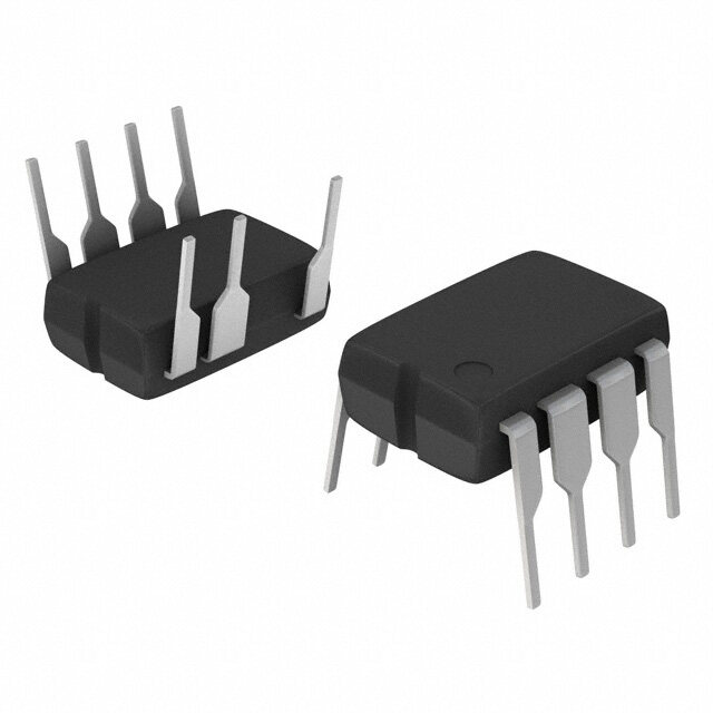
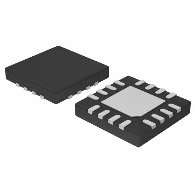
| 供应商器件封装 | 8-SON 裸露焊盘(3x3) |
| 其它名称 | 296-16675-1 |
| 内部驱动器 | 是 |
| 功率耗散 | 370 mW |
| 包装 | 剪切带 (CT) |
| 单位重量 | 23 mg |
| 商标 | Texas Instruments |
| 安装类型 | 表面贴装 |
| 安装风格 | SMD/SMT |
| 封装 | Reel |
| 封装/外壳 | 8-VDFN 裸露焊盘 |
| 封装/箱体 | VSON-8 |
| 工作温度 | -40°C ~ 85°C |
| 工作频率 | 1 MHz |
| 工厂包装数量 | 3000 |
| 恒压 | - |
| 恒流 | 是 |
| 拓扑 | PWM,升压(升压) |
| 拓扑结构 | Boost |
| 最大工作温度 | + 85 C |
| 最大电源电流 | 65 uA |
| 最小工作温度 | - 40 C |
| 标准包装 | 1 |
| 电压-电源 | 1.8 V ~ 6 V |
| 电压-输出 | 16.9V |
| 类型 | Inductive |
| 类型-初级 | 背光 |
| 类型-次级 | 白色 LED |
| 系列 | TPS61043 |
| 输入电压 | 1.8 V to 6 V |
| 输出数 | 1 |
| 输出电流 | 60 mA |
| 输出端数量 | 1 Output |
| 输出类型 | Constant Current |
| 频率 | 1MHz |


- 商务部:美国ITC正式对集成电路等产品启动337调查
- 曝三星4nm工艺存在良率问题 高通将骁龙8 Gen1或转产台积电
- 太阳诱电将投资9.5亿元在常州建新厂生产MLCC 预计2023年完工
- 英特尔发布欧洲新工厂建设计划 深化IDM 2.0 战略
- 台积电先进制程称霸业界 有大客户加持明年业绩稳了
- 达到5530亿美元!SIA预计今年全球半导体销售额将创下新高
- 英特尔拟将自动驾驶子公司Mobileye上市 估值或超500亿美元
- 三星加码芯片和SET,合并消费电子和移动部门,撤换高东真等 CEO
- 三星电子宣布重大人事变动 还合并消费电子和移动部门
- 海关总署:前11个月进口集成电路产品价值2.52万亿元 增长14.8%


PDF Datasheet 数据手册内容提取
Product Sample & Technical Tools & Support & Folder Buy Documents Software Community TPS61043 SLVS465C–DECEMBER2003–REVISEDFEBRUARY2016 TPS61043 Constant Current LED Driver 1 Features 3 Description • CurrentSourceWith18-VOvervoltageProtection The TPS61043 is a high-frequency boost converter 1 with constant current output that drives white LEDs or • Powersupto4LEDsinSeries similar. The LED current is set with the external • InputVoltageRange:1.8Vto6V sense resistor (R ) and is directly regulated by the S • Internal30-VSwitch feedback pin (FB) that regulates the voltage across the sense resistor R to 252 mV (typical). To control • Upto85%Efficiency S LED brightness, the LED current can be pulsed by • PreciseBrightnessControlUsingPWMSignalor applying a PWM (pulse width modulated) signal with AnalogSignal a frequency range of 100 Hz to 50 kHz to the control • SwitchingFrequencyupto1MHz pin (CTRL). To allow higher flexibility, the device can be configured so that the brightness is controlled by • InternalPowerMOSFETSwitch400mA an analog signal as well, as described in Application • OperatesWithSmallOutputCapacitorsDownto Information. To avoid possible leakage currents 100nF through the LEDs during shutdown, the control pin • DisconnectsLEDsDuringShutdown (CTRL) disables the device and disconnects the LEDs from ground. For maximum safety during • NoLoadQuiescentCurrent38 µATypical operation, the output has integrated overvoltage • ShutdownCurrent0.1 µATypical protection that prevents damage to the device by • AvailableinaSmall3-mm× 3-mmQFNPackage limiting the output voltage to typically 18 V in case of a high-impedance output (for example, faulty LED). 2 Applications The TPS61043 device provides a solution for applications where higher LED currents or more than • WhiteLEDSupplyforDisplayBacklightand fourLEDsinseriesmustbepowered. Sidelightin – PDAs,PocketPCs,SmartPhones DeviceInformation(1) – HandheldDevices PARTNUMBER PACKAGE BODYSIZE(NOM) – CellularPhones TPS61043 VSON(8) 3.00mm×3.00mm (1) For all available packages, see the orderable addendum at theendofthedatasheet. TypicalApplication L1 4.7µH D1 (A) CO 100 nF VIN 3 8 25 V 1.8 V to 6 V VIN SW 5 7 CTRLOVP CIN 6 1 4.7 µF GND LED 4 2 FB RS RS Enable/PWM Brightness 13Ω Control 100 Hz to 50 kHz (A)Outputcapacitorvalueslike1µFandlarger,reducetheLEDripplecurrentandimprovelineregulation. 1 An IMPORTANT NOTICE at the end of this data sheet addresses availability, warranty, changes, use in safety-critical applications, intellectualpropertymattersandotherimportantdisclaimers.PRODUCTIONDATA.
TPS61043 SLVS465C–DECEMBER2003–REVISEDFEBRUARY2016 www.ti.com Table of Contents 1 Features.................................................................. 1 9 ApplicationandImplementation........................ 12 2 Applications........................................................... 1 9.1 ApplicationInformation............................................12 3 Description............................................................. 1 9.2 TypicalApplication..................................................15 4 RevisionHistory..................................................... 2 9.3 SystemExamples...................................................19 5 PinConfigurationandFunctions......................... 3 10 PowerSupplyRecommendations..................... 22 6 Specifications......................................................... 3 11 Layout................................................................... 22 6.1 AbsoluteMaximumRatings......................................3 11.1 LayoutGuidelines.................................................22 6.2 ESDRatings..............................................................4 11.2 LayoutExample....................................................22 6.3 RecommendedOperatingConditions.......................4 11.3 ThermalConsiderations........................................22 6.4 ThermalInformation..................................................4 12 DeviceandDocumentationSupport................. 23 6.5 ElectricalCharacteristics...........................................4 12.1 DeviceSupport......................................................23 6.6 TypicalCharacteristics..............................................6 12.2 DocumentationSupport........................................23 7 ParameterMeasurementInformation..................7 12.3 CommunityResources..........................................23 12.4 Trademarks...........................................................23 8 DetailedDescription.............................................. 8 12.5 ElectrostaticDischargeCaution............................23 8.1 Overview...................................................................8 12.6 Glossary................................................................23 8.2 FunctionalBlockDiagram.........................................8 13 Mechanical,Packaging,andOrderable 8.3 FeatureDescription...................................................9 Information........................................................... 23 8.4 DeviceFunctionalModes........................................10 4 Revision History ChangesfromRevisionB(May2015)toRevisionC Page • ChangedimageobjectinFigure25. ................................................................................................................................... 22 • AddedCommunityResourcessection................................................................................................................................. 23 ChangesfromRevisionA(December2003)toRevisionB Page • AddedPinConfigurationandFunctionssection,ESDRatingstable,FeatureDescriptionsection,DeviceFunctional Modes,ApplicationandImplementationsection,PowerSupplyRecommendationssection,Layoutsection,Device andDocumentationSupportsection,andMechanical,Packaging,andOrderableInformationsection .............................. 1 2 SubmitDocumentationFeedback Copyright©2003–2016,TexasInstrumentsIncorporated ProductFolderLinks:TPS61043
TPS61043 www.ti.com SLVS465C–DECEMBER2003–REVISEDFEBRUARY2016 5 Pin Configuration and Functions DRBPackage 8-PINVSON TopView LED 1 8 SW RS 2 Exposed 7 OVP Thermal† VIN 3 Die Pad 6 GND FB 4 5 CTRL † The exposed thermal die pad is connected to GND. PinFunctions PIN I/O DESCRIPTION NAME NO. CTRL 5 I CombinedenableandPWMcontrolpin.IfCTRLisconstantlypulledhigh,thedeviceisenabledandtheinternal LEDswitch(Q2)isconstantlyturnedon.WhenCTRLispulledtoGND,thedeviceisdisabled.ApplyaPWM signal(100Hzto50kHz)tothispintocontrolthebrightnessoftheLEDs FB 4 I Feedback.FBregulatestheLEDcurrentthroughthesenseresistorbyregulatingthevoltageacrossR to S 252mV. GND 6 GND LED 1 I InputoftheLEDswitch(Q2).ConnecttheLEDstothispin. OVP 7 I Overvoltageprotection.OVPisconnectedtotheoutputcapacitoroftheconverter. RS 2 O OutputoftheinternalLEDswitch.ThesenseresistorthatprogramstheLEDcurrentisconnectedtoRS. SW 8 I Drainoftheintegratedswitch(Q1) VIN 3 I Inputsupplypin. 6 Specifications 6.1 Absolute Maximum Ratings overoperatingfree-airtemperaturerange(unlessotherwisenoted)(1) MIN MAX UNIT SupplyVoltages,v (2) –0.3 7 V (VIN) Voltages,V ,V ,V –0.3 Vin+0.3 V (Rs) (CTRL) (FB) Voltages,V ,V (2) 30 V (SW) (LED) Voltage,V 30 V (OVP) Operatingjunctiontemperature –40 150 °C Leadtemperature(soldering,10sec) 260 260 °C Storagetemperature,T –65 150 °C stg (1) StressesbeyondthoselistedunderAbsoluteMaximumRatingsmaycausepermanentdamagetothedevice.Thesearestressratings only,whichdonotimplyfunctionaloperationofthedeviceattheseoranyotherconditionsbeyondthoseindicatedunderRecommended OperatingConditions.Exposuretoabsolute-maximum-ratedconditionsforextendedperiodsmayaffectdevicereliability. (2) Allvoltagevaluesarewithrespecttonetworkgroundterminal. Copyright©2003–2016,TexasInstrumentsIncorporated SubmitDocumentationFeedback 3 ProductFolderLinks:TPS61043
TPS61043 SLVS465C–DECEMBER2003–REVISEDFEBRUARY2016 www.ti.com 6.2 ESD Ratings VALUE UNIT Humanbodymodel(HBM),perANSI/ESDA/JEDECJS-001(1) ±2000 V(ESD) Electrostaticdischarge Charged-devicemodel(CDM),perJEDECspecificationJESD22- ±750 V C101(2) (1) JEDECdocumentJEP155statesthat500-VHBMallowssafemanufacturingwithastandardESDcontrolprocess. (2) JEDECdocumentJEP157statesthat250-VCDMallowssafemanufacturingwithastandardESDcontrolprocess. 6.3 Recommended Operating Conditions MIN NOM MAX UNIT V Inputvoltage 1.8 6 V I T Operatingambienttemperature –40 85 °C A T Operatingjunctiontemperature –40 125 °C J 6.4 Thermal Information TPS61043 THERMALMETRIC(1) DRB(VSON) UNIT 8PINS R Junction-to-ambientthermalresistance 48.6 °C/W θJA R Junction-to-case(top)thermalresistance 66.9 °C/W θJC(top) R Junction-to-boardthermalresistance 23.8 °C/W θJB ψ Junction-to-topcharacterizationparameter 1.5 °C/W JT ψ Junction-to-boardcharacterizationparameter 23.9 °C/W JB R Junction-to-case(bottom)thermalresistance 5.2 °C/W θJC(bot) (1) Formoreinformationabouttraditionalandnewthermalmetrics,seetheICPackageThermalMetricsapplicationreport,SPRA953. 6.5 Electrical Characteristics V =3.6V,CTRL=V,T =–40°Cto+85°C typicalvaluesareatT =25°C(unlessotherwisenoted) I I A , A PARAMETER TESTCONDITIONS MIN TYP MAX UNIT SUPPLYCURRENT V Inputvoltagerange 1.8 6 V I I OperatingquiescentcurrentintoVIN I =0mA,notswitching 38 65 µA (Q) O I Shutdowncurrent CTRL=GND 0.1 1 µA O(sd) V Under-voltagelockoutthreshold V falling 1.5 1.7 V UVLO I CTRL V CTRLhighlevelinputvoltage 1.3 V IH V CTRLlowlevelinputvoltage 0.3 V IL I CTRLinputleakagecurrent CTRL=GNDorVIN 0.1 µA Ikg t MinimimCTRLpulsewitdhtoenable CTRL=lowtohigh 500 us on t MinimumCTRLpulsewidthtodisable CTRL=hightolow 10 32 ms off f PWMswitchingfrequencyappliedtoCTRL 0.1 50 kHz (CTRL) D PWMdutycycleappliedtoCTRL 1% 100% (CTRL) POWERSWITCHANDCURRENTLIMIT(SW) V Maximumswitchvoltage 30 V S r MOSFETON-resistance V =3.6V;I =200mA 300 600 mΩ ds(ON) I (SW) I MOSFETleakagecurrent V =28V 0.1 10 µA lkg (SW) I MOFSETcurrentlimit 320 400 480 mA LIM T Powerswitchmaximumon-time V =15V 4.5 µs ON O T Powerswitchminimumoff-time 400 ns OFF 4 SubmitDocumentationFeedback Copyright©2003–2016,TexasInstrumentsIncorporated ProductFolderLinks:TPS61043
TPS61043 www.ti.com SLVS465C–DECEMBER2003–REVISEDFEBRUARY2016 Electrical Characteristics (continued) V =3.6V,CTRL=V,T =–40°Cto+85°C typicalvaluesareatT =25°C(unlessotherwisenoted) I I A , A PARAMETER TESTCONDITIONS MIN TYP MAX UNIT LEDSWITCHANDCURRENTLIMIT(LED) V Maximumswitchvoltage 30 V S I MaximumLEDswitchcurrent 60 mA (LED) r MOSFETON-resistance V =3.6V;I =20mA 1 2 Ω ds(ON) I SW I MOSFETleakagecurrent V =28V 0.1 10 µA lkg (LED) OUTPUT V Outputvoltagerange OVPconnected V 16.9 V O I I Feedbackinputbiascurrent(1) V =0.252V 100 nA (FB) (FB) V Feedbacktrippointvoltage 1.8V≤V ≤6.0V 244 252 260 mV FB I V Outputovervoltageprotection V rising 17 18 19 V (OVP) O V Outputovervoltageprotectionhysteresis 3.65 V hys(OVP) I OVPinputcurrent V =15V 17 23 µA (OVP) O (1) Thefeedbackinputishigh-impedanceMOSFETGateinput. Copyright©2003–2016,TexasInstrumentsIncorporated SubmitDocumentationFeedback 5 ProductFolderLinks:TPS61043
TPS61043 SLVS465C–DECEMBER2003–REVISEDFEBRUARY2016 www.ti.com 6.6 Typical Characteristics Table1.TableofGraphs FIGURE V Feedbackvoltage vsTemperature Figure1 (FB) I Feedbackcurrent vsTemperature Figure2 (FB) r MainswitchQ1 vsTemperature Figure3 ds(on) vsInputvoltage Figure4 LEDswitchQ2 vsTemperature Figure5 vsInputvoltage Figure6 I AverageLEDcurrent vsPWMdutycycleonCTRLpin Figure7 LED 260 60 oltage - mV 222255552468 VCC = 3.7 V urrent - nA 2400 VCC = 3.6 V V C ack 250 ack 0 db 248 db V - Fee(fb) 222444246 I - Fee(fb) --4200 VCC = 5 V VCC = 2.4 V 240 -60 -40 -15 10 35 60 85 -40 -15 10 35 60 85 TA - Free-Air Temperature - °C TA - Free-Air Temperature - °C Figure1.FeedbackVoltagevsTemperature Figure2.FeedbackCurrentvsTemperature 500 600 Wm VCC = 3.6 V Wm TA = 27°C − 450 − 500 e e c c n n sta 400 sta 400 si si e e e R 350 e R 300 at at St St n- 300 n- 200 O O − − n) 250 n) 100 o o ds( ds( r r 200 0 −40 −15 10 35 60 85 1.8 2.4 3.0 3.6 4.2 4.8 5.4 6.0 TA − Free-Air Temperature − °C VI − Input Voltage − V Figure3.r MainSwitch(Q1)vsTemperature Figure4.r MainSwitch(Q1)vsInputVoltage ds(on) ds(ON) 1.6 3.0 We - 11..45 VCC = 3.6 V We - 2.5 TA = 25°C c c n n a 1.3 a st st 2.0 esi 1.2 esi R R e 1.1 e 1.5 at at St 1.0 St n- n- 1.0 O 0.9 O - on) 0.8 - on) 0.5 ds( 0.7 ds( r r 0.6 0.0 -40 -15 10 35 60 85 1.8 2.4 3.0 3.6 4.2 4.8 5.4 6.0 TA - Free-Air Temperature - °C VI - Input Voltage - V Figure5.r LEDSwitch(Q2)vsTemperature Figure6.r LEDSwitch(Q2)vsInputVoltage ds(on) ds(on) 6 SubmitDocumentationFeedback Copyright©2003–2016,TexasInstrumentsIncorporated ProductFolderLinks:TPS61043
TPS61043 www.ti.com SLVS465C–DECEMBER2003–REVISEDFEBRUARY2016 20 A m 15 nt - e urr ut C 10 fPWM = 100 Hz fPWM = 50 kHz p ut O - O 5 fPWM = 25 kHz I 0 0 20 40 60 80 100 Duty Cycle - % Figure7.AverageLEDCurrentvsPWMDutyCycleonCTRLPin 7 Parameter Measurement Information L1 4.7 µH D1 CO 1 µF VIN 3 8 25 V 1.8 V to 6 V VIN SW 5 7 CTRLOVP CIN 6 1 4.7 µF GND LED 4 2 FB RS L1 = Murata LQH32CN4R7 (4.7 µH) D1 = Zetex Schottky ZHCS400 RS Enable/PWM Brightness 13Ω CIN= 4.7 µF X5R 20% JMK212BJ475MG-T Control 100 Hz to 50 kHz COUT= 1 µF X7R 10% TMK316BJ105KL-T Figure8. Schematic Copyright©2003–2016,TexasInstrumentsIncorporated SubmitDocumentationFeedback 7 ProductFolderLinks:TPS61043
TPS61043 SLVS465C–DECEMBER2003–REVISEDFEBRUARY2016 www.ti.com 8 Detailed Description 8.1 Overview The TPS61043 operates like a standard boost converter but regulates the voltage across the sense resistor (RS) instead of the output voltage. This gives an accurate regulated LED current independent of the input voltage and number of LEDs connected. With integrated overvoltage protection (OVP) the TPS61043 is configured as a current source with overvoltage protection ideally suited to drive LEDs. The device can generate output voltages of up to 18 V and has an internal 400mA MOSFET switch (Q1). This allows several LEDs to be connected in series to the output. The internal LED switch (Q2) in series with the LEDs has a maximum current rating of 60 mA and disconnects the LEDs from ground during shutdown. The LED switch is driven by a PWM signal applied to the control pin (CTRL), which directly controls the LED brightness. With this control method the LED brightnessdependsonthePWMdutycycleonlyandisindependentofthePWMfrequencyandamplitude. 8.2 Functional Block Diagram EN EN SW VIN UVLO VREF Bias 0.252 V Q1 Control Gate Logic Driver Thermal Shutdown OVP Enable EN Current R1 CTRL Control Limit 1080 kΩ Logic Softstart R2 4.5 µs Max 25 kΩ On Time PWM GND Gate Drive Overvoltage Protection + - 0.4 V LED Q2 Error Comparator FB - 400 ns Min RS VREF + Off Time 8 SubmitDocumentationFeedback Copyright©2003–2016,TexasInstrumentsIncorporated ProductFolderLinks:TPS61043
TPS61043 www.ti.com SLVS465C–DECEMBER2003–REVISEDFEBRUARY2016 8.3 Feature Description 8.3.1 Operation The TPS61043 operates like a standard boost converter but regulates the voltage across the sense resistor (R ) S instead of the output voltage. This gives an accurate regulated LED current independent of the input voltage and number of LEDs connected. With integrated overvoltage protection (OVP) the TPS61043 is configured as a current source with overvoltage protection ideally suited to drive LEDs. The device can generate output voltages of up to 16.9 V if the OVP-function is used and has an internal 400 mA MOSFET switch (Q1). This allows up to four LEDs to be connected in series to the output. The internal LED switch (Q2) in series with the LEDs has a maximum current rating of 60 mA and disconnects the LEDs from ground during shutdown. The LED switch is driven by a PWM signal applied to the control pin (CTRL), which directly controls the LED brightness. With this control method the LED brightness depends on the PWM duty cycle only and is independent of the PWM frequency and amplitude. If the OVP-function is not needed, the device can be used to generate output voltages upto28V. 8.3.2 BoostConverter The boost converter operates in a pulse frequency modulation (PFM) scheme with constant peak current control. This control scheme maintains high efficiency over the entire load current range and with a switching frequency of up to 1 MHz, enables the use of small external components. The converter monitors the sense voltage across R with the feedback pin (FB) and, when the feedback voltage falls below the reference voltage (252 mV typ), S the main switch turns on and the current ramps up. The main switch turns off when the inductor current reaches the internally set peak current of 400 mA (typ). Refer to the Peak Current Control (Boost Converter) section for more information. The second criteria that turns off the main switch is the maximum on-time of 4.5 µs (typ). This limits the maximum on-time of the converter in extreme conditions. As the switch is turned off the external Schottkydiodeisforwardbiased,deliveringthestoredinductorenergytotheoutput.Themainswitchremainsoff until the minimum off time of 400 ns (typ) has passed and the feedback voltage is below the reference voltage again. Using this PFM peak current control scheme, the converter operates in discontinuous conduction mode (DCM)wheretheswitchingfrequencydependsontheinductor,inputandoutputvoltage,andLEDcurrent.Lower LED currents reduce the switching frequency, which results in high efficiency over the entire LED current range. This regulation scheme is inherently stable, allowing a wide range for the selection of the inductor and output capacitor. 8.3.3 PeakCurrentControl(BoostConverter) The internal switch is turned on until the inductor current reaches the DC current limit (I ) of 400 mA (typ) . Due LIM to the internal current limit delay of 100 ns (typ) the actual current exceeds the DC current limit threshold by a smallamount.Thetypicalpeakcurrentlimitcanbecalculated: V I (cid:3)I (cid:2) I(cid:1)100ns P(typ) (LIM) L (1) V I =400mA+ I ´100ns P L (2) Thehighertheinputvoltageandthelowertheinductorvalue,thegreaterthecurrentlimitovershoot. 8.3.4 Softstart All inductive step-up converters exhibit high in-rush current during start-up if no special precautions are taken. This can cause voltage drops at the input rail during start-up, which may result in an unwanted or premature systemshutdown. The TPS61043 limits this in-rush current during start-up by increasing the current limit in two steps starting from I /4 for 256 switch cycles to I /2 for the next 256 switch cycles and then full current limit. See Figure 16 for LIM LIM typicalstart-upbehavior. Copyright©2003–2016,TexasInstrumentsIncorporated SubmitDocumentationFeedback 9 ProductFolderLinks:TPS61043
TPS61043 SLVS465C–DECEMBER2003–REVISEDFEBRUARY2016 www.ti.com Feature Description (continued) 8.3.5 Control(CTRL) TheCTRLpinservestwofunctions.Oneistheenableanddisableofthedevice.TheotheristhePWMcontrolof the internal LED switch (Q2). The CTRL pin can be used as a standard enable pin for the device if no PWM signal is applied to the CTRL pin. To enable the device, the CTRL pin must be pulled high for a time period of at least 500 µs. The device starts with the Softstart cycle. Pulling the CTRL pin to GND for a time period ≥32 ms disables the device, disconnecting the LEDs from GND by opening the LED switch (Q2) to avoid any LED leakagecurrent.SeeFigure9 fortheCTRLpintiming. tp toff ton ton High Low Minimum Minimum On-Time t Off-Time to Enable to Disable the Device the Device (50 µs) D = tp/t (32 ms) Figure9. CTRLTimingDiagram To enable the device, the CTRL signal must be high for 500 µs (see Figure 9). The PWM signal can then be applied with a pulse width (t ) greater or smaller than t . To force the device into shutdown mode, the CTRL p ON signal must be low for at least 32 ms. Requiring the CTRL pin to be low for 32 mS before the device enters shutdown allows for PWM dimming frequencies as low as 100 Hz. The device is enabled again when a CTRL signal is high for a period of 500 µs minimum. See Figure 7 for the PWM duty cycle versus LED current characteristic. The internal LED switch (Q2) is driven by the PWM signal when applied to the CTRL pin. Applying a PWM signal in the range of 100 Hz to 50 kHz allows the LED current to be pulsed with the duty cycle of the PWM signal. The CTRL pin accepts a PWM duty cycle from D = 1% to 100%. Duty cycles below 1% are also possible with the restrictionthatthedeviceisforcedintoshutdownastheofftimeoftheappliedPWMsignalexceeds10ms. When a PWM signal is applied to the CTRL pin the LED switch (Q2) turns on immediately. The internal error comparator is disabled for 400 ns. This 400 ns delay time is required to establish the correct voltage level across thesenseresistorR aftertheLEDswitch(Q2)isclosed. S To achieve good LED current accuracy and linearity, the switching frequency of the converter must be higher thanthePWMfrequencyappliedtotheCTRLpin.ThisCTRLpinmustbeterminated. 8.4 Device Functional Modes 8.4.1 OvervoltageProtection(OVP) As with any current source, the output voltage rises as the output impedance increases as for example with a disconnected load. To prevent the output voltage from exceeding the maximum main switch (Q1) voltage rating, an overvoltage protection (OVP) circuit is integrated. With an OVP threshold voltage of 19 V maximum, up to 4 LEDs can be connected in series. This allows the use of a cheaper output capacitor with a 25 V voltage rating. When the output voltage exceeds the OVP threshold voltage, (Q1) turns off. The converter switch remains off until the output voltage falls below the OVP threshold voltage. As long as the output voltage is below the OVP threshold the converter continues its normal operation, until the output voltage exceeds the OVP threshold again. If overvoltage protection is not needed, then the OVP pin should be connected to GND. In this case the TPS61043canbeusedtogenerateoutputvoltagesupto28V. 10 SubmitDocumentationFeedback Copyright©2003–2016,TexasInstrumentsIncorporated ProductFolderLinks:TPS61043
TPS61043 www.ti.com SLVS465C–DECEMBER2003–REVISEDFEBRUARY2016 Device Functional Modes (continued) 8.4.2 UndervoltageLockout An undervoltage lockout feature prevents mis-operation of the device at input voltages below 1.5 V (typical). As long as the input voltage is below the undervoltage threshold the device remains off, with the main MOSFET switch(Q1)andtheLEDswitch(Q2)open. 8.4.3 ThermalShutdown An internal thermal shutdown is implemented in the TPS61043 that shuts down the device if the typical junction temperature of 160°C is exceeded. If the device is in thermal shutdown mode, the main MOSFET switch (Q1) andtheLEDswitch(Q2)areopen. Copyright©2003–2016,TexasInstrumentsIncorporated SubmitDocumentationFeedback 11 ProductFolderLinks:TPS61043
TPS61043 SLVS465C–DECEMBER2003–REVISEDFEBRUARY2016 www.ti.com 9 Application and Implementation NOTE Information in the following applications sections is not part of the TI component specification, and TI does not warrant its accuracy or completeness. TI’s customers are responsible for determining suitability of components for their purposes. Customers should validateandtesttheirdesignimplementationtoconfirmsystemfunctionality. 9.1 Application Information Table2.PossibleDiodes(orEquivalent) COMPONENTSUPPLIER REVERSEVOLTAGE ONSemiconductorMBR0530 30V ONSemiconductorMBR0520 20V ToshibaCRS02 30V ZetexZHCS400 40V 9.1.1 Efficiency The overall efficiency of the application depends on the specific application conditions and mainly on the selection of the inductor. A lower inductor value increases the switching frequency and switching losses yielding in a lower efficiency. A lower inductor dc resistance has lower copper losses, giving a higher efficiency. Therefore, the efficiency can typically vary ±5% depending on the selected inductor. and can be used as a guideline for the application efficiency. These curves show the typical efficiency powering four LEDs using a 4.7- µH inductor with just 1,2 mm height. The efficiency curve in and show the efficiency delivering the power to the LEDsratherthantheoverallconverterefficiencyandiscalculatedas: V (cid:1)I (cid:1)(cid:2) LED LED V (cid:1)I I I (3) 9.1.2 SettingtheLEDCurrent The converter regulates the LED current by regulating the voltage across the current sense resistor (R ). The S voltageacrossthesenseresistorisregulatedtotheinternalreferencevoltageofV =252mV. (FB) 3 8 VIN SW PWM 5 7 CTRL OVP 100 Hz to 50 kHz 6 1 GND LED 4 2 FB RS R s Figure10. SettingtheLEDCurrent TheLEDcurrentcanbecalculated: V 0.252V I = FB = LED R R S S (4) 12 SubmitDocumentationFeedback Copyright©2003–2016,TexasInstrumentsIncorporated ProductFolderLinks:TPS61043
TPS61043 www.ti.com SLVS465C–DECEMBER2003–REVISEDFEBRUARY2016 The current programming method is used when the brightness of the LEDs is fixed or controlled by a PWM signal applied to the CTRL pin. When using a PWM signal on the CTRL pin, the LED brightness is only dependent on the PWM duty cycle, independent of the PWM frequency, or amplitude, which simplifies the system. 9.1.3 AnalogControlSignalforBrightnessControl Alternatively,ananalogvoltagecanbeusedaswelltocontroltheLEDbrightness. 3 8 VIN SW Enable: CTRL= High 5 7 CTRL OVP Disable: CTRL= Low 6 1 GND LED 4 2 FB RS R1 VADJ I1 R (Brightness Control) PWM Signal Rs Vs R2 C Optional Filter for the use of a PWM Signal Figure11. SettingtheLEDCurrentUsinganAnalogControlSignal In Figure 11 the LED current is determined by the voltage applied to R2 (V ) and the selection of R1, R2 and ADJ the sense resistor (R ). In this configuration, the LED current is linear controlled instead of pulsed as in the S configurationbefore.Toselecttheresistorvaluesfollowingstepsarerequired. 1. SelectthevoltageV toturntheLEDsoff,forexample,3.3V ADJ(max) 2. SelectthevoltageV toturntheLEDsfullyon,forexample,0V ADJ(min) 3. SelectthemaximumandminimumLEDcurrentI andI ,forexample,I =20mA,I =0mA O(max) O(min) O(max) O(min) 4. Calculate R2 to achieve a feedback current in the range of I = 3 µA to 10 µA as the LEDs are fully turned 1 on: V -V R2= ref ADJ(min) I 1 (5) 5. CalculateR1 I ´R2+V -I ´R2-V R1= Vref´ O(max) ADJ(min) O(min) ADJ(max) V ´I +V ´I -V ´I -V ´I ADJ(max) O(max) ref O(min) ADJ(min) O(min) ref O(max) (6) 6. Calculatethesensevoltage(V )atmaximumLEDcurrent S R1 R1 V = V ´(1+ )- ´V S ref ADJ(min) R2 R2 (7) 7. Calculatetherequiredsenseresistor(R ) S V R = S S I O(max) (8) Copyright©2003–2016,TexasInstrumentsIncorporated SubmitDocumentationFeedback 13 ProductFolderLinks:TPS61043
TPS61043 SLVS465C–DECEMBER2003–REVISEDFEBRUARY2016 www.ti.com 9.1.4 PWMControlWithSeparateEnable The control pin (CTRL) combines the enable function as well as the PWM brightness control function in one pin. For some systems an independent enable function is required. One way to implement this is to use the brightnesscontrolconfigurationasshownintheprevioussectionFigure11. OtherpossiblesolutionsareshowninFigure12,Figure13,Figure14. 3 8 VIN SW PWM Brightness Control 5 7 CTRL OVP 100 Hz to 50 kHz 6 1 GND LED Enable (EN) 4 FB RS 2 Figure12. SeparateEnableandPWMControlUsingaSchottkyDiode 3 VIN SW 8 PWM Brightness Control 5 CTRL OVP 7 100 Hz to 50 kHz 6 1 GND LED 4 2 FB RS Enable (EN) Figure13. SeparateEnableandPWMControlUsingaTransistor PWM Brightness Control 3 8 VIN SW 100 Hz to 50 kHz 5 7 CTRL OVP Enable (EN) 6 1 GND LED 4 2 FB RS Figure14. SeparateEnableandPWMControlUsinganANDGate 14 SubmitDocumentationFeedback Copyright©2003–2016,TexasInstrumentsIncorporated ProductFolderLinks:TPS61043
TPS61043 www.ti.com SLVS465C–DECEMBER2003–REVISEDFEBRUARY2016 9.2 Typical Application L1 4.7µH D1 (A) CO 100 nF VIN 3 8 25 V 1.8 V to 6 V VIN SW 5 7 CTRLOVP CIN 6 1 4.7 µF GND LED 4 2 FB RS RS Enable/PWM Brightness 13Ω Control 100 Hz to 50 kHz (A)Outputcapacitorvalueslike1µFandlarger,reducetheLEDripplecurrentandimprovelineregulation. Figure15. TypicalApplicationSchematic 9.2.1 DesignRequirements Forthisdesignexample,usetheparameterslistedinTable3astheinputparameters. Table3.DesignParameters DESIGNPARAMETER TYPICALVALUE InputVoltage 1.8Vto6V OutputVoltage V to16V IN Dimmingfrequency 0.1to50kHz 9.2.2 DetailedDesignProcedure 9.2.2.1 InductorSelection,MaximumLoadCurrent,andSwitchingFrequency The PFM peak current control scheme of the TPS61043 is inherently stable. The inductor value does not affect the stability of the regulator. The selection of the inductor together with the nominal LED current, input, and outputvoltageoftheapplicationdeterminestheswitchingfrequencyoftheconverter. The first step is to calculate the maximum load current the converter can support using the selected inductor. The inductor value has less effect on the maximum available load current and is only of secondary order. A good inductor value to start with is 4.7 µH. Depending on the application, inductor values down to 1 µH can be used. The maximum inductor value is determined by the maximum on time of the switch of 4.5 µs (typical). The peak current limit of 400 mA (typical) must be reached within this 4.5 µs for proper operation. The maximum load current of the converter is determined at the operation point where the converter starts to enter the continuous conductionmode.Theconvertermustalwaysoperateindiscontinuousconductionmodetomaintainregulation. Depending on the time period of the inductor current fall time being larger or smaller compared to the minimum offtimeoftheconverter(400nstyp),themaximumloadcurrentcanbecalculated. Inductorfalltime: I ´L t = p f V -V O I where • t ≥400ns (9) f I ´V I =h´ P I LOAD(max) 2´V O (10) Copyright©2003–2016,TexasInstrumentsIncorporated SubmitDocumentationFeedback 15 ProductFolderLinks:TPS61043
TPS61043 SLVS465C–DECEMBER2003–REVISEDFEBRUARY2016 www.ti.com I2 ´L´V I =h´ P I LOAD(max) (V -V)´(2´I ´L+2´400ns´V) O I P I where • L=selectedinductorvalue • η=expectedconverterefficiency.Typicallybetween70%to85% (11) V I =400mA+ I ´100ns P L (12) (PeakinductorcurrentasdescribedinthePeakCurrentControl(BoostConverter) section) Theaboveformulacontainstheexpectedconverterefficiencythatallowscalculatingtheexpectedmaximumload current the converter can support. The efficiency can be taken out of the efficiency graphs shown in and or 80% canbeusedasanaccurateestimation. If the converter can support the desired LED current, the next step is to calculate the converter switching frequency at the operation point, which must be ≤1 MHz. Also the converter switching frequency should be much higher than the applied PWM frequency at the CTRL pin to avoid nonlinear brightness control. Assuming the converter shows no double pulses or pulse bursts (Figure 17 and Figure 18) on the switch node (SW) the switchingfrequencyattheoperationpointcanbecalculatedas: 2(cid:1)IO(cid:1)(cid:6)VO(cid:3)VI(cid:2)VF(cid:7) ƒs(cid:4) (cid:5)1MHz 2 (cid:6) VI (cid:7) ILIM(cid:2) L (cid:1)100ns (cid:1)L where • I =minimumswitchcurrentlimit(320mAtypical) LIM • L=selectedinductorvalue • I =nominalloadorLEDcurrent O • V =Rectifierdiodeforwardvoltage(typically0.3V) (13) F The smaller the inductor value, the higher the switching frequency of the converter but the lower the efficiency. The selected inductor must have a saturation current that meets the maximum peak current of the converter as calculated in Peak Current Control (Boost Converter). Use the maximum value for I (480 mA) for this LIM calculation. Another important inductor parameter is the DC resistance. The lower the DC resistance the higher theefficiencyoftheconverter.SeeTable4andFigure20toFigure24foraselectionofinductors. Table4.PossibleInductors(orEquivalent) INDUCTORVALUE COMPONENTSUPPLIER SIZE 10µH muRataLQH43CN100K01 4.5mm×3.2mm×2.6mm 4.7µH muRataLQH32CN4R7M11 3.2mm×2.5mm×2mm 10µH CoilcraftDO1605T-103MX 5.5mm×4.1mm×1.8mm 4.7µH SumidaCDRH3D16-4R7 3.8mm×3.8mm×1.8mm 3.3µH SumidaCMD4D11-3R3 3.5mm×5.3mm×1.2mm 4.7µH SumidaCMD4D11-4R7 3.5mm×5.3mm×1.2mm 3.3µH SumidaCMD4D11-3R3 3.5mm×5.3mm×1.2mm 4.7µH CoiltronicsSD12-4R7 5.2mm×5.2mm×1.2mm 3.3µH CoilcraftLPO1704-332M 6.6mm×5.5mm×1mm 4.7µH CoilcraftLPO1704-472M 6.6mm×5.5mm×1mm 16 SubmitDocumentationFeedback Copyright©2003–2016,TexasInstrumentsIncorporated ProductFolderLinks:TPS61043
TPS61043 www.ti.com SLVS465C–DECEMBER2003–REVISEDFEBRUARY2016 9.2.2.2 OutputCapacitorSelectionandLineRegulation For better output voltage filtering, a low ESR output capacitor is recommended. Ceramic capacitors have a low ESRvalue,butdependingontheapplication,tantalumcapacitorscanbeused. The selection of the output capacitor value directly influences the output voltage ripple of the converter which also influences line regulation. The larger the output voltage ripple, the larger the line regulation, which means that the LED current changes if the input voltage changes. If a certain change in LED current gives a noticeable changeinLEDbrightness,dependsontheLEDmanufacturerandontheapplication.Applicationsrequiringgood lineregulation≤1%/V(typ)mustuseoutputcapacitorvalues ≥1µF. SeeTable5andFigure20toFigure24fortheselectionoftheoutputcapacitor. Assuming the converter does not show double pulses or pulse bursts (see Figure 17 and Figure 18) on the switchnode(SW),theoutputvoltagerippleiscalculatedas: (cid:7) (cid:5) VI (cid:6) (cid:9) I (cid:11)(cid:11) ILIM(min)(cid:2) L (cid:1)100ns (cid:1)L(cid:11)(cid:11) (cid:1)VO(cid:4)COO(cid:1)(cid:11)(cid:11)ƒ1s(cid:3) VO(cid:2)VF(cid:3)VI (cid:11)(cid:11)(cid:2)IP(cid:1)ESR (cid:8) (cid:10) where • I =minimumswitchcurrentlimit(320mAtypical) LIM(min) • L=selectedinductorvalue • I =nominalloadcurrent O • f =switchingfrequencyatthenominalloadcurrentascalculatedwithEquation13. S • V =rectifierdiodeforwardvoltage(0.3Vtypical) F • C =selectedoutputcapacitor O • ESR=outputcapacitorESRvalue (14) 9.2.2.3 InputCapacitorSelection For good input voltage filtering, low ESR ceramic capacitors are recommended. A 4.7-µF ceramic input capacitor is sufficient for most applications. For better input voltage filtering the capacitor value can be increased. Refer to Table5andFigure20toFigure24forinputcapacitorselection. Table5.PossibleInputandOutputCapacitors(orEquivalent) CAPACITOR VOLTAGERATING COMPONENTSUPPLIER COMMENTS 4.7µF/X5R/0805 6.3V TayoYudenJMK212BY475MG C I 10µF/X5R/0805 6.3V TayoYudenJMK212BJ106MG C I 100nF Any C O 220nF Any C O 470nF Any C O 1.0µF/X7R/1206 25V TayoYudenTMK316BJ105KL C O 1.0µF/X7R/1206 35V TayoYudenGMK316BJ105KL C O 4.7µF/X5R/1210 25V TayoYudenTMK325BJ475MG C O 9.2.2.4 DiodeSelection To achieve high efficiency a Schottky diode must be used. The current rating of the diode must meet the peak current rating of the converter as it is calculated in the peak current control section. Use the maximum value for I forthiscalculation.SeeTable6andFigure20toFigure24fortheSchottkydiodeselection. LIM Table6.PossibleDiodes(orEquivalent) COMPONENTSUPPLIER REVERSEVOLTAGE ONSemiconductorMBR0530 30V ONSemiconductorMBR0520 20V Copyright©2003–2016,TexasInstrumentsIncorporated SubmitDocumentationFeedback 17 ProductFolderLinks:TPS61043
TPS61043 SLVS465C–DECEMBER2003–REVISEDFEBRUARY2016 www.ti.com Table6.PossibleDiodes(orEquivalent)(continued) COMPONENTSUPPLIER REVERSEVOLTAGE ToshibaCRS02 30V ZetexZHCS400 40V 9.2.3 ApplicationCurves Vsw Vout 5V/Div 10V/Div Vout 500mV/Div CTRL 1V/Div LED Current 20mA/Div Input Current 100mA/Div 50µs/Div 2.5µs/Div Figure16.Soft-Start Figure17. PFMOperation Vsw 5V/VDsiwv 5V/Div Vout 50mV/Div Vout 500mV/Div LED Current 20mA/Div LED Current 20mA/Div 2.5µs/Div 25µs/Div Figure18.BustModeOperation Figure19.PWMDimming 18 SubmitDocumentationFeedback Copyright©2003–2016,TexasInstrumentsIncorporated ProductFolderLinks:TPS61043
TPS61043 www.ti.com SLVS465C–DECEMBER2003–REVISEDFEBRUARY2016 9.3 System Examples 9.3.1 TPS61043With1-mmTotalSystemHeight TPS61043isdesignedfrom3Vto6VinputfordrivingLEDwith1-mmtotalsystemheight. L1 4.7 µH D1 Coilcraft LPO1704-472 ZHCS400 CO VIN 1 µF 3 V to 6 V 3 VIN SW 8 5 7 CTRL OVP C(IN) 4.7 µF 6 GND LED 1 4 FB RS 2 RS Enable/PWM Brightness 13Ω Control 100 HZ to 50 kHz Figure20. TPS61043With1-mmTotalSystemHeight 9.3.2 TPS61043WithLowLEDRippleCurrentandHigherAccuracyUsinga4.7-µFOutputCapacitor TPS61043 is designed from 3 V to 6 V input for driving LED with low LED ripple current and higher accuracy usinga4.7-µFoutputcapacitor. L1 4.7 µH D1 SUMIDACMD4D11 ZHCS400 CO 4.7 µF VIN= 3 V to 6 V 3 8 VIN SW 5 7 CTRL OVP C(IN) 4.7 µF 6 GND LED 1 4 2 FB RS RS Enable/PWM Brightness 13Ω Control 100 HZ to 50 kHz Figure21. TPS61043WithLowLEDRippleCurrentandHigherAccuracyUsinga4.7-µFOutputCapacitor Copyright©2003–2016,TexasInstrumentsIncorporated SubmitDocumentationFeedback 19 ProductFolderLinks:TPS61043
TPS61043 SLVS465C–DECEMBER2003–REVISEDFEBRUARY2016 www.ti.com System Examples (continued) 9.3.3 TPS61043Powering3LEDs TPS61043isdesignedfrom3Vto6Vinputfordriving3LEDsinseries. L1 4.7 µH D1 Coilcraft LPO1704-472 ZHCS400 CO 1 µF VIN= 2.7 V to 6 V 3 VIN SW 8 5 7 CTRL OVP CIN 6 1 4.7 µF GND LED 4 FB RS 2 RS Enable/PWM Brightness 13Ω Control 100 Hz to 50 kHz Figure22. TPS61043Powering3LEDs 9.3.4 AdjustableBrightnessControlUsinganAnalogVoltage TPS61043 is designed from 3 V to 6 V input for driving LED with adjustable brightness control using an analog voltage. L1 D1 4.7 µH ZHCS400 CO 100 nF VIN= 3 V to 6 V 3 8 VIN SW C(IN) 5 CTRL OVP 7 4.7 µF 6 GND LED 1 4 2 FB RS R101 kΩ RS Analog Brightness Control 13Ω 3.3 V =LED Off 0 V =ILED = 20 mA R2 120 kΩ Figure23. AdjustableBrightnessControlUsinganAnalogVoltage 20 SubmitDocumentationFeedback Copyright©2003–2016,TexasInstrumentsIncorporated ProductFolderLinks:TPS61043
TPS61043 www.ti.com SLVS465C–DECEMBER2003–REVISEDFEBRUARY2016 System Examples (continued) 9.3.5 AlternativeAdjustableBrightnessControlUsingPWMSignal TPS61043isdesignedfordrivingLEDwithadjustablebrightnesscontrolusingananalogvoltage. L1 D1 4.7 µH ZHCS400 CO 100 nF VIN= 3 V to 6 V 3 VIN SW 8 5 7 CTRL OVP CIN 6 1 4.7 µF GND LED 4 FB RS 2 R101 kΩ RS 3.3 V PWM Signal 13Ω 0 % LEDs on R R2 100 % LEDs Off C 120 kΩ Figure24. AlternativeAdjustableBrightnessControlUsingPWMSignal Copyright©2003–2016,TexasInstrumentsIncorporated SubmitDocumentationFeedback 21 ProductFolderLinks:TPS61043
TPS61043 SLVS465C–DECEMBER2003–REVISEDFEBRUARY2016 www.ti.com 10 Power Supply Recommendations The device is designed to operate from an input voltage supply range between 1.8 V and 6 V. The input power supply’s output current needs to be rated according to the supply voltage, output voltage and output current of TPS61043. 11 Layout 11.1 Layout Guidelines In all switching power supplies the layout is an important step in the design, especially at high peak currents and switching frequencies. If the layout is not carefully done, the regulator might show noise problems and duty cycle jitter. The input capacitor should be placed as close as possible to the input pin for good input voltage filtering. The inductor and diode must be placed as close as possible to the switch pin to minimize noise coupling into other circuits. It is important to connect the output capacitor directly across the diode cathode pin and ground rather than connecting the output capacitor across the LEDs. This minimizes EMI. Because the feedback pin and networkisahigh-impedancecircuit,thefeedbacknetworkshouldberoutedawayfromtheinductor. 11.2 Layout Example GND VIN CIN FB VIN RS LED 4 3 2 1 R SENSE TPS61043 L LED 5 6 7 8 CTRL GND OVP SW COUT DIODE Figure25. LayoutExample 11.3 Thermal Considerations The TPS61043 comes in a thermally enhanced QFN package. The package includes a thermal pad improving thethermalcapabilitiesofthepackage.See QFN/SONPCBAttachment (SLUA271). The thermal resistance junction to ambient R of the QFN package greatly depends on the PCB layout. Using ΘJA thermal vias and wide PCB traces improves the thermal resistance R . Under normal operation conditions no ΘJA PCBviasarerequiredforthethermalpad.However,thethermalpadmustbesolderedtothePCB. 22 SubmitDocumentationFeedback Copyright©2003–2016,TexasInstrumentsIncorporated ProductFolderLinks:TPS61043
TPS61043 www.ti.com SLVS465C–DECEMBER2003–REVISEDFEBRUARY2016 12 Device and Documentation Support 12.1 Device Support 12.1.1 Third-PartyProductsDisclaimer TI'S PUBLICATION OF INFORMATION REGARDING THIRD-PARTY PRODUCTS OR SERVICES DOES NOT CONSTITUTE AN ENDORSEMENT REGARDING THE SUITABILITY OF SUCH PRODUCTS OR SERVICES OR A WARRANTY, REPRESENTATION OR ENDORSEMENT OF SUCH PRODUCTS OR SERVICES, EITHER ALONEORINCOMBINATIONWITHANYTIPRODUCTORSERVICE. 12.2 Documentation Support 12.2.1 RelatedDocumentation Forrelateddocumentationseethefollowing: QFN/SONPCBAttachment,SLUA271 12.3 Community Resources The following links connect to TI community resources. Linked contents are provided "AS IS" by the respective contributors. They do not constitute TI specifications and do not necessarily reflect TI's views; see TI's Terms of Use. TIE2E™OnlineCommunity TI'sEngineer-to-Engineer(E2E)Community.Createdtofostercollaboration amongengineers.Ate2e.ti.com,youcanaskquestions,shareknowledge,exploreideasandhelp solveproblemswithfellowengineers. DesignSupport TI'sDesignSupport QuicklyfindhelpfulE2Eforumsalongwithdesignsupporttoolsand contactinformationfortechnicalsupport. 12.4 Trademarks E2EisatrademarkofTexasInstruments. Allothertrademarksarethepropertyoftheirrespectiveowners. 12.5 Electrostatic Discharge Caution Thesedeviceshavelimitedbuilt-inESDprotection.Theleadsshouldbeshortedtogetherorthedeviceplacedinconductivefoam duringstorageorhandlingtopreventelectrostaticdamagetotheMOSgates. 12.6 Glossary SLYZ022—TIGlossary. Thisglossarylistsandexplainsterms,acronyms,anddefinitions. 13 Mechanical, Packaging, and Orderable Information The following pages include mechanical, packaging, and orderable information. This information is the most current data available for the designated devices. This data is subject to change without notice and revision of thisdocument.Forbrowser-basedversionsofthisdatasheet,refertotheleft-handnavigation. Copyright©2003–2016,TexasInstrumentsIncorporated SubmitDocumentationFeedback 23 ProductFolderLinks:TPS61043
PACKAGE OPTION ADDENDUM www.ti.com 6-Feb-2020 PACKAGING INFORMATION Orderable Device Status Package Type Package Pins Package Eco Plan Lead/Ball Finish MSL Peak Temp Op Temp (°C) Device Marking Samples (1) Drawing Qty (2) (6) (3) (4/5) TPS61043DRBR ACTIVE SON DRB 8 3000 Green (RoHS NIPDAU Level-2-260C-1 YEAR -40 to 85 AQN & no Sb/Br) TPS61043DRBT ACTIVE SON DRB 8 250 Green (RoHS NIPDAU Level-2-260C-1 YEAR -40 to 85 AQN & no Sb/Br) TPS61043DRBTG4 ACTIVE SON DRB 8 250 Green (RoHS NIPDAU Level-2-260C-1 YEAR -40 to 85 AQN & no Sb/Br) (1) The marketing status values are defined as follows: ACTIVE: Product device recommended for new designs. LIFEBUY: TI has announced that the device will be discontinued, and a lifetime-buy period is in effect. NRND: Not recommended for new designs. Device is in production to support existing customers, but TI does not recommend using this part in a new design. PREVIEW: Device has been announced but is not in production. Samples may or may not be available. OBSOLETE: TI has discontinued the production of the device. (2) RoHS: TI defines "RoHS" to mean semiconductor products that are compliant with the current EU RoHS requirements for all 10 RoHS substances, including the requirement that RoHS substance do not exceed 0.1% by weight in homogeneous materials. Where designed to be soldered at high temperatures, "RoHS" products are suitable for use in specified lead-free processes. TI may reference these types of products as "Pb-Free". RoHS Exempt: TI defines "RoHS Exempt" to mean products that contain lead but are compliant with EU RoHS pursuant to a specific EU RoHS exemption. Green: TI defines "Green" to mean the content of Chlorine (Cl) and Bromine (Br) based flame retardants meet JS709B low halogen requirements of <=1000ppm threshold. Antimony trioxide based flame retardants must also meet the <=1000ppm threshold requirement. (3) MSL, Peak Temp. - The Moisture Sensitivity Level rating according to the JEDEC industry standard classifications, and peak solder temperature. (4) There may be additional marking, which relates to the logo, the lot trace code information, or the environmental category on the device. (5) Multiple Device Markings will be inside parentheses. Only one Device Marking contained in parentheses and separated by a "~" will appear on a device. If a line is indented then it is a continuation of the previous line and the two combined represent the entire Device Marking for that device. (6) Lead/Ball Finish - Orderable Devices may have multiple material finish options. Finish options are separated by a vertical ruled line. Lead/Ball Finish values may wrap to two lines if the finish value exceeds the maximum column width. Important Information and Disclaimer:The information provided on this page represents TI's knowledge and belief as of the date that it is provided. TI bases its knowledge and belief on information provided by third parties, and makes no representation or warranty as to the accuracy of such information. Efforts are underway to better integrate information from third parties. TI has taken and continues to take reasonable steps to provide representative and accurate information but may not have conducted destructive testing or chemical analysis on incoming materials and chemicals. TI and TI suppliers consider certain information to be proprietary, and thus CAS numbers and other limited information may not be available for release. Addendum-Page 1
PACKAGE OPTION ADDENDUM www.ti.com 6-Feb-2020 In no event shall TI's liability arising out of such information exceed the total purchase price of the TI part(s) at issue in this document sold by TI to Customer on an annual basis. Addendum-Page 2
PACKAGE MATERIALS INFORMATION www.ti.com 2-Feb-2016 TAPE AND REEL INFORMATION *Alldimensionsarenominal Device Package Package Pins SPQ Reel Reel A0 B0 K0 P1 W Pin1 Type Drawing Diameter Width (mm) (mm) (mm) (mm) (mm) Quadrant (mm) W1(mm) TPS61043DRBR SON DRB 8 3000 330.0 12.4 3.3 3.3 1.1 8.0 12.0 Q2 TPS61043DRBT SON DRB 8 250 180.0 12.4 3.3 3.3 1.1 8.0 12.0 Q2 PackMaterials-Page1
PACKAGE MATERIALS INFORMATION www.ti.com 2-Feb-2016 *Alldimensionsarenominal Device PackageType PackageDrawing Pins SPQ Length(mm) Width(mm) Height(mm) TPS61043DRBR SON DRB 8 3000 367.0 367.0 35.0 TPS61043DRBT SON DRB 8 250 210.0 185.0 35.0 PackMaterials-Page2
None
PACKAGE OUTLINE DRB0008A VSON - 1 mm max height SCALE 4.000 PLASTIC SMALL OUTLINE - NO LEAD 3.1 B A 2.9 PIN 1 INDEX AREA 3.1 2.9 C 1 MAX SEATING PLANE 0.05 0.08 C DIM A 0.00 OPT 1 OPT 2 1.5 0.1 (0.1) (0.2) 4X (0.23) EXPOSED (DIM A) TYP THERMAL PAD 4 5 2X 1.95 1.75 0.1 8 1 6X 0.65 0.37 8X 0.25 PIN 1 ID 0.1 C A B (OPTIONAL) (0.65) 0.05 C 0.5 8X 0.3 4218875/A 01/2018 NOTES: 1. All linear dimensions are in millimeters. Any dimensions in parenthesis are for reference only. Dimensioning and tolerancing per ASME Y14.5M. 2. This drawing is subject to change without notice. 3. The package thermal pad must be soldered to the printed circuit board for thermal and mechanical performance. www.ti.com
EXAMPLE BOARD LAYOUT DRB0008A VSON - 1 mm max height PLASTIC SMALL OUTLINE - NO LEAD (1.5) (0.65) SYMM 8X (0.6) (0.825) 8X (0.31) 1 8 SYMM (1.75) (0.625) 6X (0.65) 4 5 (R0.05) TYP ( 0.2) VIA TYP (0.23) (0.5) (2.8) LAND PATTERN EXAMPLE EXPOSED METAL SHOWN SCALE:20X 0.07 MAX 0.07 MIN ALL AROUND ALL AROUND EXPOSED EXPOSED METAL METAL SOLDER MASK METAL METAL UNDER SOLDER MASK OPENING SOLDER MASK OPENING NON SOLDER MASK SOLDER MASK DEFINED DEFINED (PREFERRED) SOLDER MASK DETAILS 4218875/A 01/2018 NOTES: (continued) 4. This package is designed to be soldered to a thermal pad on the board. For more information, see Texas Instruments literature number SLUA271 (www.ti.com/lit/slua271). 5. Vias are optional depending on application, refer to device data sheet. If any vias are implemented, refer to their locations shown on this view. It is recommended that vias under paste be filled, plugged or tented. www.ti.com
EXAMPLE STENCIL DESIGN DRB0008A VSON - 1 mm max height PLASTIC SMALL OUTLINE - NO LEAD (0.65) 4X (0.23) SYMM METAL TYP 8X (0.6) 4X (0.725) 8X (0.31) 1 8 (2.674) SYMM (1.55) 6X (0.65) 4 5 (R0.05) TYP (1.34) (2.8) SOLDER PASTE EXAMPLE BASED ON 0.125 mm THICK STENCIL EXPOSED PAD 84% PRINTED SOLDER COVERAGE BY AREA SCALE:25X 4218875/A 01/2018 NOTES: (continued) 6. Laser cutting apertures with trapezoidal walls and rounded corners may offer better paste release. IPC-7525 may have alternate design recommendations. www.ti.com
IMPORTANTNOTICEANDDISCLAIMER TI PROVIDES TECHNICAL AND RELIABILITY DATA (INCLUDING DATASHEETS), DESIGN RESOURCES (INCLUDING REFERENCE DESIGNS), APPLICATION OR OTHER DESIGN ADVICE, WEB TOOLS, SAFETY INFORMATION, AND OTHER RESOURCES “AS IS” AND WITH ALL FAULTS, AND DISCLAIMS ALL WARRANTIES, EXPRESS AND IMPLIED, INCLUDING WITHOUT LIMITATION ANY IMPLIED WARRANTIES OF MERCHANTABILITY, FITNESS FOR A PARTICULAR PURPOSE OR NON-INFRINGEMENT OF THIRD PARTY INTELLECTUAL PROPERTY RIGHTS. These resources are intended for skilled developers designing with TI products. You are solely responsible for (1) selecting the appropriate TI products for your application, (2) designing, validating and testing your application, and (3) ensuring your application meets applicable standards, and any other safety, security, or other requirements. These resources are subject to change without notice. TI grants you permission to use these resources only for development of an application that uses the TI products described in the resource. Other reproduction and display of these resources is prohibited. No license is granted to any other TI intellectual property right or to any third party intellectual property right. TI disclaims responsibility for, and you will fully indemnify TI and its representatives against, any claims, damages, costs, losses, and liabilities arising out of your use of these resources. TI’s products are provided subject to TI’s Terms of Sale (www.ti.com/legal/termsofsale.html) or other applicable terms available either on ti.com or provided in conjunction with such TI products. TI’s provision of these resources does not expand or otherwise alter TI’s applicable warranties or warranty disclaimers for TI products. Mailing Address: Texas Instruments, Post Office Box 655303, Dallas, Texas 75265 Copyright © 2020, Texas Instruments Incorporated