ICGOO在线商城 > 集成电路(IC) > PMIC - LED 驱动器 > HEF4794BT-Q100J
 Datasheet下载
- 型号: HEF4794BT-Q100J
- 制造商: NXP Semiconductors
- 库位|库存: xxxx|xxxx
- 要求:
| 数量阶梯 | 香港交货 | 国内含税 |
| +xxxx | $xxxx | ¥xxxx |
查看当月历史价格
查看今年历史价格
HEF4794BT-Q100J产品简介:
ICGOO电子元器件商城为您提供HEF4794BT-Q100J由NXP Semiconductors设计生产,在icgoo商城现货销售,并且可以通过原厂、代理商等渠道进行代购。 HEF4794BT-Q100J价格参考。NXP SemiconductorsHEF4794BT-Q100J封装/规格:PMIC - LED 驱动器, LED Driver IC 8 Output Linear Shift Register 40mA 16-SO。您可以下载HEF4794BT-Q100J参考资料、Datasheet数据手册功能说明书,资料中有HEF4794BT-Q100J 详细功能的应用电路图电压和使用方法及教程。
HEF4794BT-Q100J 是由 Nexperia USA Inc. 生产的一款符合汽车级标准(AEC-Q100 认证)的 LED 驱动器,属于 PMIC(电源管理集成电路)中的 LED 驱动器类别。该器件采用 16 引脚 DIP 封装(J 表示 DIP 封装),适用于需要稳定、可靠 LED 控制的工业与汽车电子系统。

其主要应用场景包括:
在汽车电子中,HEF4794BT-Q100J 常用于驱动仪表盘背光、车内氛围灯、状态指示灯以及控制面板上的 LED 显示模块。得益于其 AEC-Q100 认证,具备良好的温度耐受性与抗干扰能力,适合在复杂电磁环境和宽温条件下稳定运行。

此外,该芯片也可用于工业控制设备中的 LED 指示系统,如PLC模块、人机界面(HMI)、报警装置和状态显示单元。其串行输入、并行输出的移位寄存器结构支持多级级联,便于扩展控制多个 LED,实现动态灯光效果或顺序点亮功能。

由于集成恒流驱动设计,HEF4794BT-Q100J 能有效保证 LED 亮度一致性,减少外部元件数量,提升系统可靠性。同时,其工作电压范围较宽,兼容性强,适合嵌入到基于微控制器的数字控制系统中。

综上,HEF4794BT-Q100J 主要应用于对可靠性要求较高的汽车电子照明与工业指示系统,是中小规模 LED 阵列驱动的理想选择。
| 参数 | 数值 |
| 产品目录 | 集成电路 (IC) |
| 描述 | IC LED DVR SHIFT/STORE 16SOIC |
| 产品分类 | |
| 品牌 | NXP Semiconductors |
| 数据手册 | |
| 产品图片 |
|
| 产品型号 | HEF4794BT-Q100J |
| PCN封装 | |
| rohs | 无铅 / 符合限制有害物质指令(RoHS)规范要求 |
| 产品系列 | - |
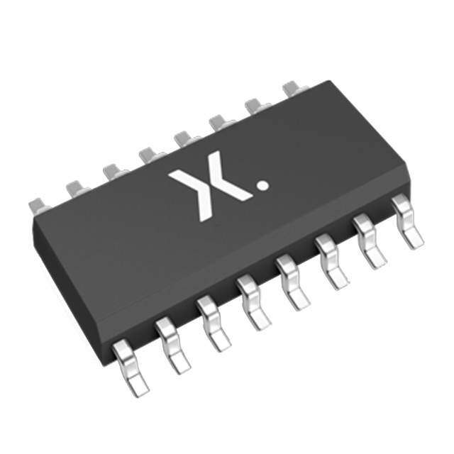
| 供应商器件封装 | 16-SO |
| 其它名称 | 568-10929-1 |
| 内部驱动器 | 是 |
| 包装 | 剪切带 (CT) |
| 安装类型 | 表面贴装 |
| 封装/外壳 | 16-SOIC(0.154",3.90mm 宽) |
| 工作温度 | -40°C ~ 125°C |
| 恒压 | - |
| 恒流 | - |
| 拓扑 | 8 位移位寄存器,开路漏极,PWM |
| 标准包装 | 1 |
| 电压-电源 | 3 V ~ 15 V |
| 电压-输出 | - |
| 类型-初级 | 通用 |
| 类型-次级 | - |
| 输出数 | 8 |
| 频率 | 28MHz |


_renders/IS31FL3199-QFLS2-TR.jpg)


PDF Datasheet 数据手册内容提取
HEF4794B-Q100 8-stage shift-and-store register LED driver Rev. 2 — 7 November 2018 Product data sheet 1. General description The HEF4794B-Q100 is an 8-stage serial shift register. It has a storage latch associated with each stage for strobing data from the serial input (D) to the parallel LED driver outputs (QP0 to QP7). Data is shifted on the positive-going clock (CP) transitions. The data in each shift register stage is transferred to the storage register when the strobe input (STR) is HIGH. Data in the storage register appears at the outputs whenever the output enable input (OE) signal is HIGH. Two serial outputs (QS1 and QS2) are available for cascading a number of HEF4794B-Q100 devices. Serial data is available at QS1 on positive-going clock edges to allow high-speed operation in cascaded systems with a fast clock rise time. The same serial data is available at QS2 on the next negative going clock edge. This is used for cascading HEF4794B-Q100 devices when the clock has a slow rise time. It operates over a recommended V power supply range of 3 V to 15 V referenced to V (usually DD SS ground). Unused inputs must be connected to V , V , or another input. DD SS This product has been qualified to the Automotive Electronics Council (AEC) standard Q100 (Grade 1) and is suitable for use in automotive applications. 2. Features and benefits • Automotive product qualification in accordance with AEC-Q100 (Grade 1) • Specified from -40 °C to +85 °C and from -40 °C to +125 °C • Fully static operation • 5 V, 10 V, and 15 V parametric ratings • Standardized symmetrical output characteristics • ESD protection: • MIL-STD-883, method 3015 exceeds 2000 V • HBM JESD22-A114F exceeds 2000 V • MM JESD22-A115-A exceeds 200 V (C = 200 pF; R = 0 Ω) • Complies with JEDEC standard JESD 13-B 3. Ordering information Table 1. Ordering information All types operate from -40 °C to +125 °C. Type number Package Name Description Version HEF4794BT-Q100 SO16 plastic small outline package; 16 leads; body width 3.9 mm SOT109-1
Nexperia HEF4794B-Q100 8-stage shift-and-store register LED driver 4. Functional diagram 3 1 CP STR QS1 9 QS2 10 2 QP0 4 D 8-STAGE SHIFT 10 QS2 QP1 5 CP 3 REGISTER 9 QP2 6 QS1 2 D QP3 7 1 8-BIT STORAGE STR REGISTER QP4 14 QP5 13 QP6 12 OE 15 OPEN-DRAIN OUTPUTS QP7 11 OE 4 5 6 7 14 13 12 11 QP0 QP2 QP4 QP6 15 QP1 QP3 QP5 QP7 001aaf111 001aag798 Fig. 1. Logic symbol Fig. 2. Functional diagram STAGE 0 STAGES 1 TO 6 STAGE 7 D D Q D Q D Q QS1 CP CP FF 0 FF 7 D Q QS2 CP CP LE LATCH D Q D Q LE LE LATCH 0 LATCH 7 STR OE QP0 QP2 QP4 QP6 QP1 QP3 QP5 QP7 aaa-029301 Fig. 3. Logic diagram HEF4794B_Q100 All information provided in this document is subject to legal disclaimers. © Nexperia B.V. 2018. All rights reserved Product data sheet Rev. 2 — 7 November 2018 2 / 14
Nexperia HEF4794B-Q100 8-stage shift-and-store register LED driver 5. Pinning information 5.1. Pinning HEF4794B STR 1 16 VDD D 2 15 OE CP 3 14 QP4 QP0 4 13 QP5 QP1 5 12 QP6 QP2 6 11 QP7 QP3 7 10 QS2 VSS 8 9 QS1 001aag800 Fig. 4. Pin configuration 5.2. Pin description Table 2. Pin description Symbol Pin Description D 2 serial input QP0 to QP7 4, 5, 6, 7, 14, 13, 12, 11 parallel output (open-drain) QS1 9 serial output QS2 10 serial output CP 3 clock input STR 1 strobe input OE 15 output enable input V 16 supply voltage DD V 8 ground (0 V) SS HEF4794B_Q100 All information provided in this document is subject to legal disclaimers. © Nexperia B.V. 2018. All rights reserved Product data sheet Rev. 2 — 7 November 2018 3 / 14
Nexperia HEF4794B-Q100 8-stage shift-and-store register LED driver 6. Functional description Table 3. Function table H = HIGH voltage level; L = LOW voltage level; X = don’t care; Z = high-impedance OFF-state; ↑ = LOW-to-HIGH clock transition; ↓ = HIGH-to-LOW clock transition. Input Parallel output Serial output CP OE STR D QP0 QPn QS1[1] QS2[2] ↑ L X X Z Z Q6S no change ↓ L X X Z Z n.c. Q7S ↑ H L X no change no change Q6S no change ↑ H H L Z QPn - 1 Q6S no change ↑ H H H L QPn - 1 Q6S no change ↓ H H H no change no change no change Q7S [1] Q6S = the data in register stage 6 before the LOW to HIGH clock transition. [2] Q7S = the data in register stage 7 before the HIGH to LOW clock transition. clock input data input strobe input output enable input internal Q0S (FF0) Z-state QP0 output internal Q6S (FF6) Z-state QP6 output serial QS1 output serial QS2 output 001aag801 Fig. 5. Timing diagram HEF4794B_Q100 All information provided in this document is subject to legal disclaimers. © Nexperia B.V. 2018. All rights reserved Product data sheet Rev. 2 — 7 November 2018 4 / 14
Nexperia HEF4794B-Q100 8-stage shift-and-store register LED driver 7. Limiting values Table 4. Limiting values In accordance with the Absolute Maximum Rating System (IEC 60134). Symbol Parameter Conditions Min Max Unit V supply voltage -0.5 +18 V DD I input clamping current V < -0.5 V or V > V + 0.5 V - ±10 mA IK I I DD V input voltage -0.5 V + 0.5 V I DD I output clamping current QSn outputs; - ±10 mA OK V < -0.5 V or V > V + 0.5 V O O DD QPn outputs; V < -0.5 V - 40 mA O I input leakage current - ±10 mA I I output current QSn outputs - ±10 mA O QPn outputs - 40 mA T storage temperature -65 +150 °C stg T ambient temperature -40 +125 °C amb P total power dissipation T = -40 °C to +125 °C tot amb SO16 package [1] - 500 mW P power dissipation per output - 100 mW [1] For SO16 package: Ptot derates linearly with 8 mW/K above 70 °C. 8. Recommended operating conditions Table 5. Recommended operating conditions Symbol Parameter Conditions Min Max Unit V supply voltage 3 15 V DD V input voltage 0 V V I DD T ambient temperature in free air -40 +125 °C amb Δt/ΔV input transition rise and fall rate V = 5 V - 3.75 μs/V DD V = 10 V - 0.5 μs/V DD V = 15 V - 0.08 μs/V DD HEF4794B_Q100 All information provided in this document is subject to legal disclaimers. © Nexperia B.V. 2018. All rights reserved Product data sheet Rev. 2 — 7 November 2018 5 / 14
Nexperia HEF4794B-Q100 8-stage shift-and-store register LED driver 9. Static characteristics Table 6. Static characteristics V = 0 V; V = V or V ; unless otherwise specified. SS I SS DD Symbol Parameter Conditions V T = -40 °C T = 25 °C T = 85 °C T = 125 °C Unit DD amb amb amb amb Min Max Min Max Min Max Min Max V HIGH-level |I | < 1 μA 5 V 3.5 - 3.5 - 3.5 - 3.5 - V IH O input voltage 10 V 7.0 - 7.0 - 7.0 - 7.0 - V 15 V 11.0 - 11.0 - 11.0 - 11.0 - V V LOW-level input |I | < 1 μA 5 V - 1.5 - 1.5 - 1.5 - 1.5 V IL O voltage 10 V - 3.0 - 3.0 - 3.0 - 3.0 V 15 V - 4.0 - 4.0 - 4.0 - 4.0 V V HIGH-level QSn outputs; 5 V 4.95 - 4.95 - 4.95 - 4.95 - V OH output voltage |I | < 1 μA O 10 V 9.95 - 9.95 - 9.95 - 9.95 - V 15 V 14.95 - 14.95 - 14.95 - 14.95 - V V LOW-level QSn outputs; 5 V - 0.05 - 0.05 - 0.05 - 0.05 V OL output voltage |I | < 1 μA O 10 V - 0.05 - 0.05 - 0.05 - 0.05 V 15 V - 0.05 - 0.05 - 0.05 - 0.05 V QPn outputs; 5 V - 0.75 - 0.75 - 1.5 - 1.5 V |I | < 20 mA O 10 V - 0.75 - 0.75 - 1.5 - 1.5 V 15 V - 0.75 - 0.75 - 1.5 - 1.5 V I HIGH-level QSn outputs OH output current V = 2.5 V 5 V - -1.7 - -1.4 - -1.1 - -1.1 mA O V = 4.6 V 5 V - -0.64 - -0.5 - -0.36 - -0.36 mA O V = 9.5 V 10 V - -1.6 - -1.3 - -0.9 - -0.9 mA O V = 13.5 V 15 V - -4.2 - -3.4 - -2.4 - -2.4 mA O I LOW-level QSn outputs OL output current V = 0.4 V 5 V 0.64 - 0.5 - 0.36 - 0.36 - mA O V = 0.5 V 10 V 1.6 - 1.3 - 0.9 - 0.9 - mA O V = 1.5 V 15 V 4.2 - 3.4 - 2.4 - 2.4 - mA O I input leakage 15 V - ±0.1 - ±0.1 - ±1.0 - ±1.0 μA I current I OFF-state QPn output 5 V - 2 - 2 - 15 - 15 μA OZ output current is HIGH; 10 V - 2 - 2 - 15 - 15 μA V = 15 V O 15 V - 2 - 2 - 15 - 15 μA I supply current I = 0 A 5 V - 5 - 5 - 150 - 150 μA DD O 10 V - 10 - 10 - 300 - 300 μA 15 V - 20 - 20 - 600 - 600 μA C input - - - - - 7.5 - - - pF I capacitance HEF4794B_Q100 All information provided in this document is subject to legal disclaimers. © Nexperia B.V. 2018. All rights reserved Product data sheet Rev. 2 — 7 November 2018 6 / 14
Nexperia HEF4794B-Q100 8-stage shift-and-store register LED driver 10. Dynamic characteristics Table 7. Dynamic characteristics V = 0 V; T = 25 °C unless otherwise specified. For test circuit, see Fig. 10. SS amb Symbol Parameter Conditions V Extrapolation formula Min Typ Max Unit DD t HIGH to LOW CP to QS1; 5 V [1] 132 ns + (0.55 ns/pF)C - 160 320 ns PHL L propagation delay see Fig. 6 10 V 53 ns + (0.23 ns/pF)C - 65 130 ns L 15 V 37 ns + (0.16 ns/pF)C - 45 90 ns L CP to QS2; 5 V 92 ns + (0.55 ns/pF)C - 120 240 ns L see Fig. 6 10 V 39 ns + (0.23 ns/pF)C - 50 100 ns L 15 V 32 ns + (0.16 ns/pF)C - 40 80 ns L t LOW to HIGH CP to QS1; 5 V [1] 102 ns + (0.55 ns/pF)C - 130 260 ns PLH L propagation delay see Fig. 6 10 V 44 ns + (0.23 ns/pF)C - 55 110 ns L 15 V 32 ns + (0.16 ns/pF)C - 40 80 ns L CP to QS2; 5 V 102 ns + (0.55 ns/pF)C - 130 260 ns L see Fig. 6 10 V 49 ns + (0.23 ns/pF)C - 60 120 ns L 15 V 37 ns + (0.16 ns/pF)C - 45 90 ns L t OFF-state to LOW CP to QPn; 5 V - 240 480 ns PZL propagation delay see Fig. 6 10 V - 80 160 ns 15 V - 55 110 ns STR to QPn; 5 V - 140 280 ns see Fig. 7 10 V - 70 140 ns 15 V - 55 110 ns t LOW to OFF-state CP to QPn; 5 V - 170 340 ns PLZ propagation delay see Fig. 6 10 V - 75 150 ns 15 V - 60 120 ns STR to QPn; 5 V - 100 200 ns see Fig. 7 10 V - 40 100 ns 15 V - 35 70 ns t enable time OE to QPn; 5 V [2] - 100 200 ns en see Fig. 8 10 V - 55 110 ns 15 V - 50 100 ns t disable time OE to QPn; 5 V [2] - 80 160 ns dis see Fig. 8 10 V - 40 80 ns 15 V - 30 60 ns t transition time QS1, QS2; 5 V [1][3] 35 ns + (1.00 ns/pF)C - 85 170 ns t L see Fig. 6 10 V 19 ns + (0.42 ns/pF)C - 40 80 ns L 15 V 16 ns + (0.28 ns/pF)C - 30 60 ns L t pulse width CP LOW and 5 V 60 30 - ns W HIGH; see Fig. 6 10 V 30 15 - ns 15 V 24 12 - ns STR HIGH; 5 V 80 40 - ns see Fig. 7 10 V 60 30 - ns 15 V 24 12 - ns HEF4794B_Q100 All information provided in this document is subject to legal disclaimers. © Nexperia B.V. 2018. All rights reserved Product data sheet Rev. 2 — 7 November 2018 7 / 14
Nexperia HEF4794B-Q100 8-stage shift-and-store register LED driver Symbol Parameter Conditions V Extrapolation formula Min Typ Max Unit DD t set-up time D to CP; see Fig. 9 5 V 60 30 - ns su 10 V 20 10 - ns 15 V 15 5 - ns t hold time D to CP; see Fig. 9 5 V +5 -15 - ns h 10 V 20 5 - ns 15 V 20 5 - ns f maximum clock CP; see Fig. 6 5 V 5 10 - MHz clk(max) frequency 10 V 11 22 - MHz 15 V 14 28 - MHz [1] The typical values of the propagation delay and transition times are calculated from the extrapolation formulas shown (CL in pF). [2] ten is the same as tPZL and tdis is the same as tPLZ [3] tt is the same as tTLH and tTHL Table 8. Dynamic power dissipation P can be calculated from the formulas shown. V = 0 V; t = t ≤ 20 ns; T = 25 °C. D SS r f amb Symbol Parameter V Typical formula Where DD 2 P dynamic power dissipation 5 V P = 1 200 x f + Σ(f x C ) x V μW f = input frequency in MHz; D D i o L DD i 10 V P = 5 550 x f + Σ(f x C ) x V 2 μW fo = output frequency in MHz; D i o L DD C = output load capacitance in pF; 2 L 15 V PD = 15 000 x fi + Σ(fo x CL) x VDD μW Σ(fo × CL) = sum of the outputs; V = supply voltage in V. DD 10.1. Waveforms and test circuit 1/fclk(max) VI CP input VM VSS tW tW tPLZ tPZL VDD VY QPn output VX VOL tPLH tPHL VOH 90 % QS1 output VM 10 % VOL tTLH tTHL tPLH tPHL VOH 90 % QS2 output VM 10 % VOL tTLH tTHL 001aag222 Parallel output measurement points are given in Table 9. V and V are typical output voltage levels that occur with the output load. OL OH Fig. 6. Propagation delay clock (CP) to output (QPn, QS1, QS2), clock pulse width and maximum clock frequency HEF4794B_Q100 All information provided in this document is subject to legal disclaimers. © Nexperia B.V. 2018. All rights reserved Product data sheet Rev. 2 — 7 November 2018 8 / 14
Nexperia HEF4794B-Q100 8-stage shift-and-store register LED driver Table 9. Measurement points Supply Input Output V V V V V DD M M X Y 5 V to 15 V 0.5V 0.5V 0.1V 0.9V DD DD O O VI CP input VM VSS VI STR input VM VSS tW tPLZ tPZL VDD VY QPn output VOL VX 001aag802 Measurement points are given in Table 9. V is the typical output voltage level that occurs with the output load. OL Fig. 7. Strobe (STR) to output (QPn) propagation delays and the strobe pulse width VI OE input VM VSS tPLZ tPZL outpuVt DD VY LOW to OFF-state OFF-state to LOW VOL VX outputs outputs outputs enabled disabled enabled 001aag803 Measurement points are given in Table 9. V is the typical output voltage level that occurs with the output load. OL Fig. 8. Enable and disable times for input OE VI CP input VM VSS tsu tsu th th VI D input VM VSS VDD QPn output VOL 001aag805 Measurement points are given in Table 9. The shaded areas indicate when the input is permitted to change for predictable output performance. V is the typical output voltage level that occurs with the output load. OL Fig. 9. Set-up and hold times for the data input (D) HEF4794B_Q100 All information provided in this document is subject to legal disclaimers. © Nexperia B.V. 2018. All rights reserved Product data sheet Rev. 2 — 7 November 2018 9 / 14
Nexperia HEF4794B-Q100 8-stage shift-and-store register LED driver VI 90 % input pulse 10 % VSS tr tf VEXT VDD RL VI VO G DUT RT CL 001aag804 Test data is given in Table 10. Definitions for test circuit: DUT - Device Under Test. R = Load resistance. L C = load capacitance. L R = Termination resistance should be equal to output impedance of Z of the pulse generator. T o V = External voltage for measuring switching times. EXT Fig. 10. Test circuit for measuring switching times Table 10. Test data Supply Input V Load EXT V V t, t t , t t , t C R DD I r f PLZ PZL PLH PHL L L 5 V to 15 V V ≤ 20 ns V open 50 pF 1 kΩ DD DD 11. Application information VDD VDD QP0 QP7 QP0 QP7 D HEF4794B S2 D HEF4794B S2 OE STR CP OE STR CP PWM dimmer input CONTROL AND SYNC CIRCUITRY 001aag806 data clock from remote control panel Fig. 11. Application example: serial-to-parallel data converting LED drivers HEF4794B_Q100 All information provided in this document is subject to legal disclaimers. © Nexperia B.V. 2018. All rights reserved Product data sheet Rev. 2 — 7 November 2018 10 / 14
Nexperia HEF4794B-Q100 8-stage shift-and-store register LED driver 12. Package outline SO16: plastic small outline package; 16 leads; body width 3.9 mm SOT109-1 D E A X c y H E v M A Z 16 9 Q A 2 A 1 (A 3 ) A pin 1 index θ L p 1 8 L e w M detail X b p 0 2.5 5 mm scale DIMENSIONS (inch dimensions are derived from the original mm dimensions) UNIT mAax . A 1 A 2 A 3 b p c D (1) E (1) e H E L L p Q v w y Z (1) θ 0.25 1.45 0.49 0.25 10.0 4.0 6.2 1.0 0.7 0.7 mm 1.75 0.25 1.27 1.05 0.2 5 0.25 0.1 0.10 1.25 0.36 0.19 9.8 3.8 5.8 0.4 0.6 0.3 8 o 0.010 0.057 0.019 0.0100 0.39 0.16 0.244 0.039 0.028 0.028 0 o inches 0.069 0.01 0.05 0.041 0.01 0.01 0.004 0.004 0.049 0.014 0.0075 0.38 0.15 0.228 0.016 0.020 0.012 Note 1. Plastic or metal protrusions of 0.15 mm (0.006 inch) maximum per side are not included. OUTLINE REFERENCES EUROPEAN ISSUE DATE VERSION IEC JEDEC JEITA PROJECTION 99-12-27 SOT109-1 076E07 MS-012 03-02-19 Fig. 12. Package outline SOT109-1 (SO16) HEF4794B_Q100 All information provided in this document is subject to legal disclaimers. © Nexperia B.V. 2018. All rights reserved Product data sheet Rev. 2 — 7 November 2018 11 / 14
Nexperia HEF4794B-Q100 8-stage shift-and-store register LED driver 13. Revision history Table 11. Revision history Document ID Release date Data sheet status Change notice Supersedes HEF4794B_Q100 v.2 20181107 Product data sheet - HEF4794B _Q100 v.1 Modifications: • The format of this data sheet has been redesigned to comply with the identity guidelines of Nexperia. • Legal texts have been adapted to the new company name where appropriate. • Fig. 5 corrected. HEF4794B _Q100 v.1 20120807 Product data sheet - - HEF4794B_Q100 All information provided in this document is subject to legal disclaimers. © Nexperia B.V. 2018. All rights reserved Product data sheet Rev. 2 — 7 November 2018 12 / 14
Nexperia HEF4794B-Q100 8-stage shift-and-store register LED driver equipment, nor in applications where failure or malfunction of an Nexperia 14. Legal information product can reasonably be expected to result in personal injury, death or severe property or environmental damage. Nexperia and its suppliers accept no liability for inclusion and/or use of Nexperia products in such equipment or applications and therefore such inclusion and/or use is at the customer's own Data sheet status risk. Quick reference data — The Quick reference data is an extract of the Document status Product Definition product data given in the Limiting values and Characteristics sections of this [1][2] status [3] document, and as such is not complete, exhaustive or legally binding. Objective [short] Development This document contains data from Applications — Applications that are described herein for any of these data sheet the objective specification for products are for illustrative purposes only. Nexperia makes no representation product development. or warranty that such applications will be suitable for the specified use without further testing or modification. Preliminary [short] Qualification This document contains data from Customers are responsible for the design and operation of their applications data sheet the preliminary specification. and products using Nexperia products, and Nexperia accepts no liability for Product [short] Production This document contains the product any assistance with applications or customer product design. It is customer’s data sheet specification. sole responsibility to determine whether the Nexperia product is suitable and fit for the customer’s applications and products planned, as well as for the planned application and use of customer’s third party customer(s). [1] Please consult the most recently issued document before initiating or Customers should provide appropriate design and operating safeguards to completing a design. minimize the risks associated with their applications and products. [2] The term 'short data sheet' is explained in section "Definitions". [3] The product status of device(s) described in this document may have Nexperia does not accept any liability related to any default, damage, costs changed since this document was published and may differ in case of or problem which is based on any weakness or default in the customer’s multiple devices. The latest product status information is available on applications or products, or the application or use by customer’s third party the internet at https://www.nexperia.com. customer(s). Customer is responsible for doing all necessary testing for the customer’s applications and products using Nexperia products in order to avoid a default of the applications and the products or of the application or Definitions use by customer’s third party customer(s). Nexperia does not accept any liability in this respect. Draft — The document is a draft version only. The content is still under internal review and subject to formal approval, which may result in Limiting values — Stress above one or more limiting values (as defined in modifications or additions. Nexperia does not give any representations or the Absolute Maximum Ratings System of IEC 60134) will cause permanent warranties as to the accuracy or completeness of information included herein damage to the device. Limiting values are stress ratings only and (proper) and shall have no liability for the consequences of use of such information. operation of the device at these or any other conditions above those given in the Recommended operating conditions section (if present) or the Short data sheet — A short data sheet is an extract from a full data sheet Characteristics sections of this document is not warranted. Constant or with the same product type number(s) and title. A short data sheet is repeated exposure to limiting values will permanently and irreversibly affect intended for quick reference only and should not be relied upon to contain the quality and reliability of the device. detailed and full information. For detailed and full information see the relevant full data sheet, which is available on request via the local Nexperia sales Terms and conditions of commercial sale — Nexperia products are office. In case of any inconsistency or conflict with the short data sheet, the sold subject to the general terms and conditions of commercial sale, as full data sheet shall prevail. published at http://www.nexperia.com/profile/terms, unless otherwise agreed in a valid written individual agreement. In case an individual agreement is Product specification — The information and data provided in a Product concluded only the terms and conditions of the respective agreement shall data sheet shall define the specification of the product as agreed between apply. Nexperia hereby expressly objects to applying the customer’s general Nexperia and its customer, unless Nexperia and customer have explicitly terms and conditions with regard to the purchase of Nexperia products by agreed otherwise in writing. In no event however, shall an agreement be customer. valid in which the Nexperia product is deemed to offer functions and qualities beyond those described in the Product data sheet. No offer to sell or license — Nothing in this document may be interpreted or construed as an offer to sell products that is open for acceptance or the grant, conveyance or implication of any license under any copyrights, patents Disclaimers or other industrial or intellectual property rights. Limited warranty and liability — Information in this document is believed Export control — This document as well as the item(s) described herein to be accurate and reliable. However, Nexperia does not give any may be subject to export control regulations. Export might require a prior representations or warranties, expressed or implied, as to the accuracy authorization from competent authorities. or completeness of such information and shall have no liability for the Translations — A non-English (translated) version of a document is for consequences of use of such information. Nexperia takes no responsibility reference only. The English version shall prevail in case of any discrepancy for the content in this document if provided by an information source outside between the translated and English versions. of Nexperia. In no event shall Nexperia be liable for any indirect, incidental, punitive, special or consequential damages (including - without limitation - lost Trademarks profits, lost savings, business interruption, costs related to the removal Notice: All referenced brands, product names, service names and or replacement of any products or rework charges) whether or not such trademarks are the property of their respective owners. damages are based on tort (including negligence), warranty, breach of contract or any other legal theory. Notwithstanding any damages that customer might incur for any reason whatsoever, Nexperia’s aggregate and cumulative liability towards customer for the products described herein shall be limited in accordance with the Terms and conditions of commercial sale of Nexperia. Right to make changes — Nexperia reserves the right to make changes to information published in this document, including without limitation specifications and product descriptions, at any time and without notice. This document supersedes and replaces all information supplied prior to the publication hereof. Suitability for use in automotive applications — This Nexperia product has been qualified for use in automotive applications. Unless otherwise agreed in writing, the product is not designed, authorized or warranted to be suitable for use in life support, life-critical or safety-critical systems or HEF4794B_Q100 All information provided in this document is subject to legal disclaimers. © Nexperia B.V. 2018. All rights reserved Product data sheet Rev. 2 — 7 November 2018 13 / 14
Nexperia HEF4794B-Q100 8-stage shift-and-store register LED driver Contents 1. General description......................................................1 2. Features and benefits..................................................1 3. Ordering information....................................................1 4. Functional diagram.......................................................2 5. Pinning information......................................................3 5.1. Pinning.........................................................................3 5.2. Pin description.............................................................3 6. Functional description.................................................4 7. Limiting values.............................................................5 8. Recommended operating conditions..........................5 9. Static characteristics....................................................6 10. Dynamic characteristics............................................7 10.1. Waveforms and test circuit........................................8 11. Application information............................................10 12. Package outline........................................................11 13. Revision history........................................................12 14. Legal information......................................................13 © Nexperia B.V. 2018. All rights reserved For more information, please visit: http://www.nexperia.com For sales office addresses, please send an email to: salesaddresses@nexperia.com Date of release: 7 November 2018 HEF4794B_Q100 All information provided in this document is subject to legal disclaimers. © Nexperia B.V. 2018. All rights reserved Product data sheet Rev. 2 — 7 November 2018 14 / 14