ICGOO在线商城 > 集成电路(IC) > PMIC - LED 驱动器 > TPS75103YFFR
 Datasheet下载
- 型号: TPS75103YFFR
- 制造商: Texas Instruments
- 库位|库存: xxxx|xxxx
- 要求:
| 数量阶梯 | 香港交货 | 国内含税 |
| +xxxx | $xxxx | ¥xxxx |
查看当月历史价格
查看今年历史价格
TPS75103YFFR产品简介:
ICGOO电子元器件商城为您提供TPS75103YFFR由Texas Instruments设计生产,在icgoo商城现货销售,并且可以通过原厂、代理商等渠道进行代购。 TPS75103YFFR价格参考¥3.67-¥8.22。Texas InstrumentsTPS75103YFFR封装/规格:PMIC - LED 驱动器, LED 驱动器 IC 4 输出 线性 PWM 调光 25mA 9-DSBGA(1.2x1.3)。您可以下载TPS75103YFFR参考资料、Datasheet数据手册功能说明书,资料中有TPS75103YFFR 详细功能的应用电路图电压和使用方法及教程。
TPS75103YFFR 是 Texas Instruments(德州仪器)推出的一款 PMIC(电源管理集成电路),属于 LED 驱动器系列。该器件专为需要高效、低功耗和高精度电流控制的应用场景设计,以下是其主要应用场景:

 1. 便携式电子设备
   - TPS75103YFFR 的低功耗特性和小型封装使其非常适合用于便携式电子设备,例如:
     - 智能手机的背光驱动
     - 平板电脑的显示屏照明
     - 可穿戴设备(如智能手表或健身追踪器)的指示灯或显示屏背光

 2. 工业控制与监控
   - 在工业领域,TPS75103YFFR 可用于驱动状态指示灯、面板显示灯或报警灯,具体包括:
     - 工业仪表的背光驱动
     - 监控设备的LED指示灯
     - 工业自动化系统中的信号灯

 3. 汽车电子
   - 该芯片支持高可靠性和宽工作电压范围,适用于汽车环境中的以下应用:
     - 仪表盘背光驱动
     - 车内氛围灯控制
     - 显示屏或导航系统的LED光源驱动

 4. 消费类电子产品
   - TPS75103YFFR 可广泛应用于各种消费类电子产品中,提供稳定且高效的LED驱动解决方案,例如:
     - 数码相机的LCD背光
     - 音频设备的指示灯或显示屏背光
     - 家用电器的状态指示灯

 5. 医疗设备
   - 在医疗领域,TPS75103YFFR 的高精度电流控制特性可用于驱动关键的LED组件,例如:
     - 医疗显示器的背光
     - 手持医疗设备的指示灯
     - 生命体征监测设备的光源

 核心优势
- 高效能:采用低dropout架构,提高整体效率。
- 精确电流控制:确保LED亮度的一致性。
- 小尺寸封装:适合空间受限的设计。
- 保护功能:内置过温保护、短路保护等,提升系统可靠性。

综上所述,TPS75103YFFR 凭借其高效、紧凑和可靠的特性,成为多种应用场景中LED驱动的理想选择。
| 参数 | 数值 |
| 产品目录 | 集成电路 (IC)光电子产品 |
| 描述 | IC LED DRIVER LINEAR 9-DSBGALED照明驱动器 Low Dropout Two- Bank LED Driver |
| 产品分类 | |
| 品牌 | Texas Instruments |
| 产品手册 | |
| 产品图片 |
|
| rohs | 符合RoHS无铅 / 符合限制有害物质指令(RoHS)规范要求 |
| 产品系列 | LED照明电子器件,LED照明驱动器,Texas Instruments TPS75103YFFR- |
| 数据手册 | |
| 产品型号 | TPS75103YFFR |
| 产品种类 | LED照明驱动器 |
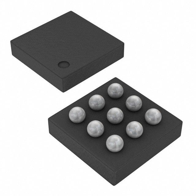
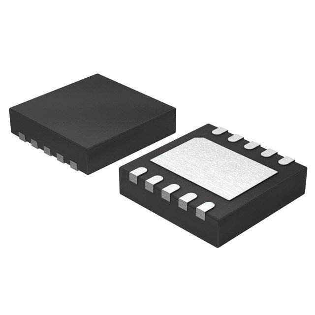
| 供应商器件封装 | 9-DSBGA(1.2x1.3) |
| 其它名称 | 296-21284-1 |
| 内部驱动器 | 是 |
| 功率耗散 | 704 mW |
| 包装 | 剪切带 (CT) |
| 商标 | Texas Instruments |
| 安装类型 | 表面贴装 |
| 安装风格 | SMD/SMT |
| 封装 | Reel |
| 封装/外壳 | 9-UFBGA,DSBGA |
| 封装/箱体 | DSBGA-9 |
| 工作温度 | -40°C ~ 85°C |
| 工厂包装数量 | 3000 |
| 恒压 | - |
| 恒流 | 是 |
| 拓扑 | 线性(LDO),PWM |
| 拓扑结构 | LDO |
| 最大工作温度 | + 85 C |
| 最大电源电流 | 0.3 mA |
| 最小工作温度 | - 40 C |
| 标准包装 | 1 |
| 电压-电源 | 2.7 V ~ 5.5 V |
| 电压-输出 | 3.6V |
| 类型 | Linear |
| 类型-初级 | 背光 |
| 类型-次级 | 颜色,白色 LED |
| 系列 | TPS75103 |
| 输入电压 | 2.7 V to 5.5 V |
| 输出数 | 4 |
| 输出电流 | 25 mA |
| 输出端数量 | 4 Output |
| 输出类型 | Constant Current |
| 频率 | - |


- 商务部:美国ITC正式对集成电路等产品启动337调查
- 曝三星4nm工艺存在良率问题 高通将骁龙8 Gen1或转产台积电
- 太阳诱电将投资9.5亿元在常州建新厂生产MLCC 预计2023年完工
- 英特尔发布欧洲新工厂建设计划 深化IDM 2.0 战略
- 台积电先进制程称霸业界 有大客户加持明年业绩稳了
- 达到5530亿美元!SIA预计今年全球半导体销售额将创下新高
- 英特尔拟将自动驾驶子公司Mobileye上市 估值或超500亿美元
- 三星加码芯片和SET,合并消费电子和移动部门,撤换高东真等 CEO
- 三星电子宣布重大人事变动 还合并消费电子和移动部门
- 海关总署:前11个月进口集成电路产品价值2.52万亿元 增长14.8%


PDF Datasheet 数据手册内容提取
Product Sample & Technical Tools & Support & Folder Buy Documents Software Community TPS75100,TPS75103,TPS75105 SBVS080J–SEPTEMBER2006–REVISEDNOVEMBER2016 TPS7510x Low Dropout, Two-Bank LED Driver With PWM Brightness Control 1 Features 3 Description • RegulatedOutputCurrentwith2%LED-to-LED The TPS7510x linear low dropout (LDO) matching 1 LED current source is optimized for low-power Matching keypad and navigation pad LED backlighting • DrivesUptoFourLEDsat25mAEachina applications. The device provides a constant current CommonCathodeTopology touptofourunmatchedLEDsorganizedintwobanks • 28-mVTypicalDropoutVoltageExtendsUsable of two LEDs each in a common-cathode topology. SupplyRangeinLi-IonBatteryApplications Without an external resistor, the current source defaults to a factory-programmable, preset current • BrightnessControlUsingPWMSignals level with ±0.5% accuracy (typical). An optional • Two2-LEDBanksWithIndependentEnableand external resistor can be used to set initial brightness PWMBrightnessControlperBank to user-programmable values with higher accuracy. • NoInternalSwitchingSignals—EliminatesEMI Brightness can be varied from off to full brightness by inputting a pulse width modulation (PWM) signal on • DefaultLEDCurrentEliminatesExternal each enable pin (ENx, where x indicates LED bank A Components or B). Each bank has independent enable and – DefaultValuesfrom3mAto10mA(in1-mA brightness control, but current matching is done to all Increments)AvailableUsingInnovativeFactory four channels concurrently. The input supply range is EEPROMProgramming ideally suited for single-cell Li-Ion battery supplies – OptionalExternalResistorcanbeUsedfor andtheTPS7510xcanprovideupto25mAperLED. High-Accuracy,User-ProgrammableCurrent No internal switching signals are used, eliminating • OvercurrentandOvertemperatureProtection troublesome electromagnetic interference (EMI). The TPS7510x is offered in an ultra-small, 9-ball, 0.4-mm • AvailableinWaferChip-ScalePackage ball-pitch wafer chip-scale package (WCSP) and a or2.50-mm×2.50-mmWSON-10 2.50-mm × 2.50-mm, 10-pin WSON package, yielding a very compact total solution size ideal for mobile 2 Applications handsets and portable backlighting applications. The • KeypadandDisplayBacklighting deviceisfullyspecifiedoverTJ=–40°Cto+85°C. • WhiteandColorLEDs DeviceInformation(1) • CellularHandsets PARTNUMBER PACKAGE BODYSIZE(NOM) • PDAsandSmartphones WSON(10) 2.50mm×2.50mm TPS7510x DSBGA(9) 1.208mmx1.208mm (1) For all available packages, see the orderable addendum at theendofthedatasheet. TypicalApplicationDiagram V BATT TPS7510x VIN D1A VENA ENA D2A VENB ENB D1B D2B I SET 1 An IMPORTANT NOTICE at the end of this data sheet addresses availability, warranty, changes, use in safety-critical applications, intellectualpropertymattersandotherimportantdisclaimers.PRODUCTIONDATA.
TPS75100,TPS75103,TPS75105 SBVS080J–SEPTEMBER2006–REVISEDNOVEMBER2016 www.ti.com Table of Contents 1 Features.................................................................. 1 8 ApplicationandImplementation........................ 10 2 Applications........................................................... 1 8.1 ApplicationInformation............................................10 3 Description............................................................. 1 8.2 TypicalApplication..................................................12 4 RevisionHistory..................................................... 2 9 PowerSupplyRecommendations...................... 14 5 PinConfigurationandFunctions......................... 3 10 Layout................................................................... 14 6 Specifications......................................................... 4 10.1 LayoutGuidelines.................................................14 6.1 AbsoluteMaximumRatings......................................4 10.2 LayoutExample....................................................14 6.2 ESDRatings..............................................................4 11 DeviceandDocumentationSupport................. 15 6.3 RecommendedOperatingConditions.......................4 11.1 DeviceSupport......................................................15 6.4 ThermalInformation..................................................4 11.2 DocumentationSupport........................................15 6.5 ElectricalCharacteristics...........................................5 11.3 RelatedLinks........................................................15 6.6 TypicalCharacteristics..............................................6 11.4 ReceivingNotificationofDocumentationUpdates15 7 DetailedDescription.............................................. 8 11.5 CommunityResources..........................................15 7.1 Overview...................................................................8 11.6 Trademarks...........................................................16 7.2 FunctionalBlockDiagram.........................................8 11.7 ElectrostaticDischargeCaution............................16 7.3 FeatureDescription...................................................9 11.8 Glossary................................................................16 7.4 DeviceFunctionalModes..........................................9 12 Mechanical,Packaging,andOrderable Information........................................................... 16 4 Revision History NOTE:Pagenumbersforpreviousrevisionsmaydifferfrompagenumbersinthecurrentversion. ChangesfromRevisionI(November2013)toRevisionJ Page • AddedDeviceInformationtable,TypicalApplicationDiagramtitletofront-pagediagram,ESDRatingstable, ThermalInformationtable,FeatureDescriptionsection,DeviceFunctionalModessection,Applicationand Implementationsection,PowerSupplyRecommendationssection,Layoutsection,DeviceandDocumentation Supportsection,andMechanical,Packaging,andOrderableInformationsection ............................................................... 1 • ChangedSONtoWSONthroughoutdocument .................................................................................................................... 1 • DeletedpinoutdrawingsfromTypicalApplicationDiagramfigure........................................................................................ 1 • ChangedI/OstatustoIfromOinD1BrowofPinFunctionstable....................................................................................... 3 • DeletedDissipationRatingstable........................................................................................................................................... 4 ChangesfromRevisionH(January2010)toRevisionI Page • ChangedtestconditionsforgroundcurrentparameterintheElectricalCharacteristics....................................................... 5 • DeletedFigure14;duplicatemechanicalimage.................................................................................................................. 12 ChangesfromRevisionG(March2009)toRevisionH Page • Revisedgroundcurrentparameter,ElectricalCharacteristics;changedsymbolfromI toI ;addedspecifications Q GND forYFFandDSKpackages.................................................................................................................................................... 5 • AddedYFFandDSKpackagespecificationsforcurrentmatchingparameter,ElectricalCharacteristics............................ 5 • Changeddiodecurrentaccuracyparameter,ElectricalCharacteristics,toreflectYFFandDSKpackagespecifications....5 • DeletedoperatingjunctiontemperaturerangespecificationfromElectricalCharacteristicstabletoeliminateredundancy.5 2 SubmitDocumentationFeedback Copyright©2006–2016,TexasInstrumentsIncorporated ProductFolderLinks:TPS75100 TPS75103 TPS75105
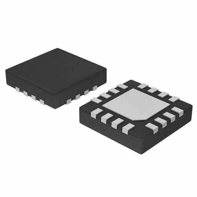
TPS75100,TPS75103,TPS75105 www.ti.com SBVS080J–SEPTEMBER2006–REVISEDNOVEMBER2016 5 Pin Configuration and Functions YFFPackage DSKPackage 9-PinDSBGA 10-PinWSON TopView TopView A3 B3 C3 ENB 1 10 I A2 B2 C2 SET ENA 2 9 V A1 B1 C1 IN D1A 3 GND 8 D1B D2A 4 7 D2B (1) GND 5 6 NC NOTE (1): Not connected PinFunctions PIN I/O DESCRIPTION NAME WCSP WSON Enablepin,BankA.DrivingthispinhighturnsonthecurrentsourcetoBankA outputs.DrivingthispinlowturnsoffthecurrentsourcetoBankAoutputs.An appliedPWMsignalreducestheLEDcurrent(between0mAandthemaximum ENA A3 2 I currentsetbyI )asafunctionofthedutycycleofthePWMsignal.ENAand SET ENBcanbetiedtogether.ENAcanbeleftOPENorconnectedtoGNDifnotused. SeetheApplicationandImplementationsectionformoredetails. D1A B3 3 O Diodesourcecurrentoutput,BankA.ConnecttoLEDanode. D2A C3 4 O Diodesourcecurrentoutput,BankA.ConnecttoLEDanode. Enablepin,BankB.DrivingthispinhighturnsonthecurrentsourcetoBankB outputs.DrivingthispinlowturnsoffthecurrentsourcetoBankBoutputs.An appliedPWMsignalreducestheLEDcurrent(between0mAandthemaximum ENB A2 1 I currentsetbyI )asafunctionofthedutycycleofthePWMsignal.ENAand SET ENBcanbetiedtogether.ENBcanbeleftOPENorconnectedtoGNDifnotused. SeetheApplicationandImplementationsectionformoredetails. V B2 9 I Supplyinput IN GND C2 5,Pad — Ground AnoptionalresistorcanbeconnectedbetweenthispinandGNDtosetthe I A1 10 I maximumcurrentthroughtheLEDs.Ifnoresistorisconnected,I defaultstothe SET SET internallyprogrammedvalue. D1B B1 8 O Diodesourcecurrentoutput,BankB.ConnecttoLEDanode. D2B C1 7 O Diodesourcecurrentoutput,BankB.ConnecttoLEDanode. NC — 6 — Notinternallyconnected Copyright©2006–2016,TexasInstrumentsIncorporated SubmitDocumentationFeedback 3 ProductFolderLinks:TPS75100 TPS75103 TPS75105
TPS75100,TPS75103,TPS75105 SBVS080J–SEPTEMBER2006–REVISEDNOVEMBER2016 www.ti.com 6 Specifications 6.1 Absolute Maximum Ratings overoperatingfree-airtemperaturerange(unlessotherwisenoted) MIN MAX UNIT V range –0.3 7 V IN V ,V ,V ,V range –0.3 V V ISET ENA ENB DX IN I forD1A,D2A,D1B,D2B 35 mA DX D1A,D2A,D1B,D2Bshort-circuitduration Indefinite Continuoustotalpowerdissipation Internallylimited Junctiontemperature,T –55 150 °C J Storagetemperature,T –55 150 °C stg 6.2 ESD Ratings VALUE UNIT Human-bodymodel(HBM),perANSI/ESDA/JEDECJS-001(1) ±2000 V Electrostaticdischarge V (ESD) Charged-devicemodel(CDM),perJEDECspecificationJESD22-C101(2) ±500 (1) JEDECdocumentJEP155statesthat500-VHBMallowssafemanufacturingwithastandardESDcontrolprocess. (2) JEDECdocumentJEP157statesthat250-VCDMallowssafemanufacturingwithastandardESDcontrolprocess. 6.3 Recommended Operating Conditions PARAMETER MIN NOM MAX UNIT V Inputvoltage 2.7 5.5 V IN I OperatingcurrentperLED 3 25 mA DX t On-timeforPWMsignal 33 µs PWM T Operatingjunctiontemperaturerange –40 85 °C J 6.4 Thermal Information TPS7510x THERMALMETRIC(1) YFF(DSBGA) DSK(WSON) UNIT 9PINS 10PINS R Junction-to-ambientthermalresistance 101.6 65.3 °C/W θJA R Junction-to-case(top)thermalresistance 1.2 54.0 °C/W θJC(top) R Junction-to-boardthermalresistance 17.6 39.5 °C/W θJB ψ Junction-to-topcharacterizationparameter 0.6 1.6 °C/W JT ψ Junction-to-boardcharacterizationparameter 17.8 39.7 °C/W JB R Junction-to-case(bottom)thermalresistance N/A 23.6 °C/W θJC(bot) (1) Formoreinformationabouttraditionalandnewthermalmetrics,seetheSemiconductorandICPackageThermalMetricsapplication report. 4 SubmitDocumentationFeedback Copyright©2006–2016,TexasInstrumentsIncorporated ProductFolderLinks:TPS75100 TPS75103 TPS75105
TPS75100,TPS75103,TPS75105 www.ti.com SBVS080J–SEPTEMBER2006–REVISEDNOVEMBER2016 6.5 Electrical Characteristics overoperatingjunctiontemperaturerange(T =–40°Cto+85°C),V =3.8V,DxAandDxB=3.3V,R =32.4kΩ,and J IN SET ENAandENB=3.8V(unlessotherwisenoted);typicalvaluesareatT =25°C A PARAMETER TESTCONDITIONS MIN TYP MAX UNIT I Shutdownsupplycurrent V =0V,V =0V 0.03 1 µA SHDN ENA,B DX DSK IDX≤5mA,VIN=3.8V 170 230 package I >5mA,V =3.8V 250 300 DX IN I Groundcurrent µA GND YFF IDX≤5mA,VIN=4.5V 170 200 package I >5mA,V =4.5V 250 300 DX IN T =25°C 0% 2% 4% A YFF Currentmatching 0% 5% ΔI package D (IDXMAX–IDXMIN/IDXMAX)×100% TA=–40°Cto+85°C DSK 0% 6% package ΔI %/ΔV Lineregulation 3.5V≤V ≤4.5V,I =5mA 2.0 %/V DX IN IN DX ΔI %/ΔV Loadregulation 1.8V≤V ≤3.5V,I =5mA 0.8 %/V DX DX DX DX Dropoutvoltageofany I =5mA 28 100 DXnom V DXcurrentsource mV DO (VDXatIDX=0.8×IDX,nom) IDXnom=15mA 70 V Referencevoltageforcurrentset 1.183 1.225 1.257 V ISET YFF 0.5% 3% I Diodecurrentaccuracy(1) ISET=open, package OPEN VDX=VIN–0.2V DSK 0.5% 4% package I I pincurrentrange 2.5 62.5 µA SET SET k I toI currentratio(1) 420 SET DX V Enablehighlevelinputvoltage 1.2 V IH V Enablelowlevelinputvoltage 0.4 V IL V =3.8V 5.0 6.1 ENA I EnablepinA(V )inputcurrent µA INA ENA V =1.8V 2.2 ENA V =3.8V 4.0 4.9 ENB I EnablepinB(V )inputcurrent µA INB ENB V =1.8V 1.8 ENB DelayfromENAandENB=lowto t Shutdowndelaytime reachshutdowncurrent 5 13 30 µs SD (I =0.1×I ) DX DX,nom Shutdown,temperatureincreasing 165 T Thermalshutdowntemperature °C SD Reset,temperaturedecreasing 140 (1) AverageofallfourI outputs. DX Copyright©2006–2016,TexasInstrumentsIncorporated SubmitDocumentationFeedback 5 ProductFolderLinks:TPS75100 TPS75103 TPS75105
TPS75100,TPS75103,TPS75105 SBVS080J–SEPTEMBER2006–REVISEDNOVEMBER2016 www.ti.com 6.6 Typical Characteristics overoperatingjunctiontemperaturerange(T =–40°Cto+85°C),V =3.8V,DxAandDxB=3.3V,R =32.4kΩ,and J IN SET ENAandENB=high(unlessotherwisenoted);typicalvaluesareatT =25°C A 25 20 3.9V 1V/div V A) 15 3.6V IN m ( UT IO 10 0.5mA/div I OUT 5 0 0 10 20 30 40 50 60 70 80 90 100 20ms/div Duty Cycle (%) Figure1.LEDCurrentvsDutyCycle(f=300Hz) Figure2.LineTransient(600-mVPulse) 1.2V 3.6V 1V/div 3.3V VIN 0.4V 1V/div ENA = ENB 20mA/div I 0.5mA/div I OUT OUT 20ms/div 20ms/div Figure4.DimmingResponse(BothChannels) Figure3.LineTransient(300-mVPulse) 25 ENA = 3.8V 20 -40°C 1.2V 0.4V A) 15 1V/div ENB m (UT +25°C IO 10 +85°C 20mA/div I OUT 5 0 20ms/div 0 0.02 0.04 0.06 0.08 0.10 0.12 0.14 0.16 0.18 0.20 V -V (V) IN OUT Figure5.DimmingResponse(SingleChannel) Figure6.OutputCurrentvsHeadroomVoltage 6 SubmitDocumentationFeedback Copyright©2006–2016,TexasInstrumentsIncorporated ProductFolderLinks:TPS75100 TPS75103 TPS75105
TPS75100,TPS75103,TPS75105 www.ti.com SBVS080J–SEPTEMBER2006–REVISEDNOVEMBER2016 Typical Characteristics (continued) overoperatingjunctiontemperaturerange(T =–40°Cto+85°C),V =3.8V,DxAandDxB=3.3V,R =32.4kΩ,and J IN SET ENAandENB=high(unlessotherwisenoted);typicalvaluesareatT =25°C A 28 28 26 Expanded Range 26 24 24 22 22 20 20 18 18 A) 16 A) 16 m m ( 14 ( 14 UT 12 UT 12 O O I 10 I 10 8 8 6 6 4 4 2 2 0 0 20 60 100 140 180 220 260 300 340 380 420 460 500 20 30 40 50 60 70 80 90 100 R (kW) R (kW) SET SET Figure7.OutputCurrentvsR Figure8.OutputCurrentvsR SET SET 180 5.4 5.3 175 5.2 -40°C +25°C A) 170 +85°C mA) 5.1 I(mQ 165 (OUT 5.0 +85°C I 4.9 +25°C 4.8 160 -40°C 4.7 155 4.6 2.5 3.0 3.5 4.0 4.5 5.0 5.5 3.4 3.9 4.4 4.9 5.4 5.9 VIN(V) VIN(V) Figure9.GroundCurrentvsInputVoltage Figure10.TPS75105OutputCurrentvsInputVoltage R =Open SET 5.4 20 5.3 18 IOUTD2B IOUTD1B 16 5.2 14 5.1 A) A) 12 m m ( 5.0 ( 10 IOUT 4.9 IOUTD2A IOUT 8 I D1A OUT 6 4.8 4 +85°C 4.7 +25°C 2 -40°C 4.6 0 -40 -20 0 20 40 60 80 85 0 0.5 1.0 1.5 2.0 2.5 3.0 3.5 4.0 Temperature (°C) V (V) OUT Figure11.TPS75105OutputCurrentvsTemperature Figure12.OutputCurrentvsOutputVoltage R =Open SET Copyright©2006–2016,TexasInstrumentsIncorporated SubmitDocumentationFeedback 7 ProductFolderLinks:TPS75100 TPS75103 TPS75105
TPS75100,TPS75103,TPS75105 SBVS080J–SEPTEMBER2006–REVISEDNOVEMBER2016 www.ti.com 7 Detailed Description 7.1 Overview The TPS7510x linear low dropout (LDO) matching LED current source is optimized for low-power keypad and navigation pad LED backlighting applications. The device provides a constant current to up to four unmatched LEDs organized in two banks of two LEDs each in a common-cathode topology. Brightness can be varied from off to full brightness by inputting a pulse width modulation (PWM) signal on each enable pin (ENx, where x indicates LED bank A or B). Each bank has independent enable and brightness control, but current matching is done to all four channels concurrently. The input supply range is ideally suited for single-cell Li-Ion battery suppliesandtheTPS7510xcanprovideupto25mAperLED. 7.2 Functional Block Diagram Controlled Current Source D1A Control ENA Logic 800kW Controlled Current Source D2A Controlled Current Source D1B ENB 1MW Control Logic VIN Controlled Current Source D2B Int/Ext ISET Set Current Sense Current Reference GND 8 SubmitDocumentationFeedback Copyright©2006–2016,TexasInstrumentsIncorporated ProductFolderLinks:TPS75100 TPS75103 TPS75105
TPS75100,TPS75103,TPS75105 www.ti.com SBVS080J–SEPTEMBER2006–REVISEDNOVEMBER2016 7.3 Feature Description 7.3.1 LoadRegulation The TPS7510x is designed to provide very tight load regulation. In the case of a fixed current source, the output loadchangeisachangeinvoltage.Tightloadregulationmeansthatoutputvoltages(LEDforwardvoltages)with large variations can be used without impacting the fixed current being sourced by the output or the output-to- output current matching. The permissible variation on the output not only allows for large variations in white LED forward voltages, but even permits the use of different color LEDs on different outputs with minimal effect on outputcurrent. 7.3.2 LineRegulation The TPS7510x is also designed to provide very tight line regulation. This architecture allows for voltage transient events to occur on the power supply (battery) without effecting the fixed output current levels or the output-to- output current matching. A prime example of such a supply transient event is the occurrence of a transmit pulse on the radio of a mobile handset. These transient pulses can cause variations of 300 mV and 600 mV on the supply to the TPS7510x. The line regulation limitation is that the lower supply voltage level of the event does not causetheinput-to-outputvoltagedifferencetodropbelowthedropoutvoltagerange. 7.4 Device Functional Modes 7.4.1 LEDON Apply1.2VormoretoENxtoturntheLEDbankon. 7.4.2 LEDOFF Applyavoltagelessthanorequalto0.4VtoENxtoturntheLEDbankoff. Copyright©2006–2016,TexasInstrumentsIncorporated SubmitDocumentationFeedback 9 ProductFolderLinks:TPS75100 TPS75103 TPS75105
TPS75100,TPS75103,TPS75105 SBVS080J–SEPTEMBER2006–REVISEDNOVEMBER2016 www.ti.com 8 Application and Implementation NOTE Information in the following applications sections is not part of the TI component specification, and TI does not warrant its accuracy or completeness. TI’s customers are responsible for determining suitability of components for their purposes. Customers should validateandtesttheirdesignimplementationtoconfirmsystemfunctionality. 8.1 Application Information The TPS7510x provides a constant current to up to four unmatched LEDs organized in two banks of two LEDs each in a common-cathode topology. Without an external resistor, the current source defaults to a factory- programmable, preset current level with ±0.5% accuracy (typical). An optional external resistor can be used to set initial brightness to user-programmable values with higher accuracy. Brightness can be varied from off to full brightness by inputting a pulse width modulation (PWM) signal on each enable pin (ENx, where x indicates LED bank A or B). Each bank has independent enable and brightness control, but current matching is done to all four channels concurrently. The input supply range is ideally suited for single-cell Li-Ion battery supplies and the TPS7510x can provide up to 25 mA per LED. No internal switching signals are used, eliminating troublesome electromagneticinterference(EMI).ThedeviceisfullyspecifiedoverT =–40°Cto+85°C. J 8.1.1 SettingtheOutputCurrentLevel The TPS7510x is a quad matched current source. Each of the four current source output levels is set by a single reference current. An internal voltage reference of 1.225 V (nominal) in combination with a resistor sets the reference current level. This reference current is then mirrored onto each of the four outputs with a ratio of typically420:1.TheresistorrequiredtosettheLEDcurrentiscalculatedusingEquation1: K´V ISET R = ISET I LED where: • Kisthecurrentratio • V istheinternalreferencevoltage ISET • I isthedesiredLEDcurrent (1) LED For example, to set the LED current level to 10mA, a resistor value of 51.1 kΩ is required. This value sets up a reference current of 23.9 μA (1.22 V / 51.1 kΩ). In turn, this reference current is mirrored to each output current source,resultinginanoutputcurrentof10mA(23.9 μA× 420). The TPS7510x offers two methods for setting the output current levels. The LED current is set either by connecting a resistor (calculated using Equation 1) from the I pin to GND, or leaving I unconnected to SET SET employ the factory-programmed R resistance. The internal programmed resistance is implemented using SET high-precision processing and yields a reference current accuracy of 0.5%, nominal. Accuracy using external resistorsissubjecttothetoleranceoftheexternalresistorandtheaccuracyoftheinternalreferencevoltage. TheTPS7510xautomaticallydetectsthepresenceofanexternalresistorbymonitoringthecurrentoutoftheI SET pin. Current levels in excess of 3 μA signify the presence of an external resistor and the device uses the external resistor to set the reference current. If the current from I is less than 3 μA, the device defaults to the preset SET internal reference set resistor. The TPS7510x is available with eight preset current levels, from 3 mA to 10 mA (per output) in 1-mA increments. Solutions using the preset internal current level eliminate an external component,therebyincreasingaccuracyandreducingcost. 10 SubmitDocumentationFeedback Copyright©2006–2016,TexasInstrumentsIncorporated ProductFolderLinks:TPS75100 TPS75103 TPS75105
TPS75100,TPS75103,TPS75105 www.ti.com SBVS080J–SEPTEMBER2006–REVISEDNOVEMBER2016 Application Information (continued) Table1.Recommended(1%Tolerance)SetResistorValues R (kΩ) I (μA) I (mA)(1) SET SET DX 511 2.4 1.0 255 4.8 2.0 169 7.2 3.0 127 9.6 4.1 102 12.0 5.0 84.5 14.5 6.1 73.2 16.7 7.0 64.9 18.9 7.9 56.2 21.8 9.2 51.1 24.0 10.1 46.4 26.4 11.1 42.2 29.0 12.2 39.2 31.3 13.1 36.5 33.6 14.1 34.0 36.0 15.1 32.4 37.8 15.9 30.1 40.7 17.1 28.7 42.7 17.9 26.7 45.9 19.3 25.5 48.0 20.2 24.3 50.4 21.2 23.2 52.8 22.2 22.1 55.4 23.3 21.5 57.0 23.9 20.5 59.8 25.1 (1) I =(V /R )×k. DX SET SET 8.1.2 LimitationsonLEDForwardVoltages The TPS7510x is a linear current source implementing LDO regulator building blocks. Therefore, to maintain accurate operation, there are some limitations to the forward (output) voltages that can be used. The first limitation is the maximum LED forward voltage. The dropout voltage must be considered because LDO technology is employed. The TPS7510x is an ultra-low dropout device with typical dropouts in the range of 30 mV at 5 mA. Care must be taken in the design to ensure that the difference between the lowest possible input voltage (for example, battery cut-off) and the highest possible forward voltage yields at least 100 mV of headroom.Headroomlevelslessthandropoutdecreasetheaccuracyofthecurrentsource(seeFigure6). The other limitation to consider is the minimum output voltage required to yield accurate operation. The current source employs NMOS MOSFETs, and a minimum forward LED voltage of approximately 1.5 V on the output is required to maintain highest accuracy. The TPS7510x is ideal for white LEDs and color LEDs with forward voltagesgreaterthan1.5V.ThisrangeincludesredLEDsthathavetypicalforwardvoltagesof1.7V. 8.1.3 UseofExternalCapacitors The TPS7510x does not require the use of any external capacitors for stable operation. Nominal stray and power-supply decoupling capacitance on the input is adequate for stable operation. Capacitors are not needed forstabilityandarethereforenotrecommendedontheoutputs. Copyright©2006–2016,TexasInstrumentsIncorporated SubmitDocumentationFeedback 11 ProductFolderLinks:TPS75100 TPS75103 TPS75105
TPS75100,TPS75103,TPS75105 SBVS080J–SEPTEMBER2006–REVISEDNOVEMBER2016 www.ti.com 8.1.4 UseofUnusedOutputsorTyingOutputsTogether Unused outputs can be left unconnected or tied to the V supply. Although open outputs are acceptable, tying IN unused outputs to the V supply increases ESD protection. Connecting unused outputs to ground violates the IN minimum recommended output voltage, results in current levels that potentially exceed the set or preset LED current,andmustbeavoided. Connecting outputs in parallel is an acceptable way of increasing the amount of LED current drive. This configurationisausefultrickwhenthehighercurrentlevelisamultipleofthepresetvalue. 8.1.5 UseofEnablePinsforPWMDimming The TPS7510x divides control of the LED outputs into two banks of two current sources each. Each bank is controlled by the use of an independent, active-high enable pin (ENA and ENB). The enable pin can be used for standard ON or OFF operation of the current source, driven by standard logic levels from processor GPIO pins, forexample.DriveENxhightoturnonthebankofLEDs;driveENxlowtoturnoffthebankofLEDs. Another use of the enable pins is for LED dimming. LED brightness is a function of the current level being driven across the diode and the time that current is being driven through the diode. The perceived brightness of an LED canbechangedbyeithervaryingthecurrentlevelor,moreeffectively,bychangingthetimeinwhichthatcurrent is present. When a PWM signal is input into the enable pin, the duty cycle (high- or on-time) determines how long the fixed current is driven across the LEDs. Reducing or increasing that duration has the effect of dimming or brightening the LED, without having to employ the more complex method of varying the current level. This techniqueisparticularlyusefulforreducingLEDbrightnessinlowambientlightconditions,whereLEDbrightness is not required, thereby decreasing current consumption. The enable pins can also be used for LED blinking, varyingblinkratesbasedonsystemstatus. Although providing many useful applications, PWM dimming does have a minimum duty cycle required to achieve the required current level. The recommended minimum on-time of the TPS7510x is approximately 33 μs. On-times less than 33 μs result in reductions in the output current by not allowing enough time for the output to reach the desired current level. Also, having both enables switching together, asynchronously, or having one enable on at all times, effects the minimum recommended on-time (see Figure 4 and Figure 5). If one enable is already on, the speed at which the other channel turns on is faster than if both channels are turning on together or if the other channel is off. Therefore, already having one channel enabled allows for approximately 10-μs to 12-μsshorterminimumon-timesfortheswitchingchannel. Unused enable pins can be left unconnected or connected to ground to minimize current consumption. Connecting unused enable pins to ground increases ESD protection. If connected to V , a small amount of IN currentdrainsthroughtheenableinput(seetheElectricalCharacteristicstable). 8.2 Typical Application TPS7510x ENA D1A Dimming PWM or CPU GPIO ENB D2A D1B V IN Li-Ion D2B Battery I SET GND R SET (optional) Figure13. TypicalApplicationDiagram 12 SubmitDocumentationFeedback Copyright©2006–2016,TexasInstrumentsIncorporated ProductFolderLinks:TPS75100 TPS75103 TPS75105
TPS75100,TPS75103,TPS75105 www.ti.com SBVS080J–SEPTEMBER2006–REVISEDNOVEMBER2016 Typical Application (continued) 8.2.1 DesignRequirements Table2showsthedesignrequirements. Table2.DesignParameters PARAMETER DESIGNREQUIREMENT Inputvoltage 3.8V NumberofLEDs 4 LEDcurrent 5mA(perLED) 8.2.2 DetailedDesignProcedure SelecttheTPS75105sothatnoexternalresistorisrequiredtosettheLEDcurrent. 8.2.3 ApplicationCurve 5.4 5.3 IOUTD2B IOUTD1B 5.2 5.1 A) m ( 5.0 OUT IOUTD2A I 4.9 I D1A OUT 4.8 4.7 4.6 -40 -20 0 20 40 60 80 85 Temperature (°C) R =open SET Figure14.TPS75105OutputCurrentvsTemperature Copyright©2006–2016,TexasInstrumentsIncorporated SubmitDocumentationFeedback 13 ProductFolderLinks:TPS75100 TPS75103 TPS75105
TPS75100,TPS75103,TPS75105 SBVS080J–SEPTEMBER2006–REVISEDNOVEMBER2016 www.ti.com 9 Power Supply Recommendations TheTPS7510xisdesignedtooperatewithaninputvoltagebetween2.7Vto5.5V. 10 Layout 10.1 Layout Guidelines Figure15demonstratesanexamplelayoutfortheWSONpackage. 10.2 Layout Example R SET ENB ENA VIN GND PLANE Figure15. LayoutExamplefortheWSON(DSK)Package 14 SubmitDocumentationFeedback Copyright©2006–2016,TexasInstrumentsIncorporated ProductFolderLinks:TPS75100 TPS75103 TPS75105
TPS75100,TPS75103,TPS75105 www.ti.com SBVS080J–SEPTEMBER2006–REVISEDNOVEMBER2016 11 Device and Documentation Support 11.1 Device Support 11.1.1 DevelopmentSupport Two evaluation modules (EVMs) are available to assist in the initial circuit performance evaluation using the TPS7510x. The TPS75105EVM-174 and TPS75105DSKEVM-529 evaluation modules (and related user guides) can be requested at the Texas Instruments website through the product folders or purchased directly from the TI eStore. 11.1.2 DeviceNomenclature PRODUCTID OPTIONS(1)(2) Xisthenominaldefaultdiodeoutputcurrent(forexample,3=3mA,5=5mA,and0=10mA). TPS7510xyyyz YYYisthepackagedesignator. Zisthereelquantity(R=3000,T=250). (1) ForthemostcurrentpackageandorderinginformationseethePackageOptionAddendumattheendofthisdocument,orseetheTI websiteatwww.ti.com. (2) Defaultsetcurrentsfrom3mAto10mAin1-mAincrementsareavailablethroughtheuseofinnovativefactoryEEPROMprogramming. Minimumorderquantitiesmayapply.Contactfactoryfordetailsandavailability. 11.2 Documentation Support 11.2.1 RelatedDocumentation Forrelateddocumentationseethefollowing: • TPS75105EVM-174EvaluationModule (SLVU182) • TPS75105DSKEVM-529EvaluationModule (SLVU334) 11.3 Related Links The table below lists quick access links. Categories include technical documents, support and community resources,toolsandsoftware,andquickaccesstosampleorbuy. Table3.RelatedLinks TECHNICAL TOOLS& SUPPORT& PARTS PRODUCTFOLDER SAMPLE&BUY DOCUMENTS SOFTWARE COMMUNITY TPS75100 Clickhere Clickhere Clickhere Clickhere Clickhere TPS75103 Clickhere Clickhere Clickhere Clickhere Clickhere TPS75105 Clickhere Clickhere Clickhere Clickhere Clickhere 11.4 Receiving Notification of Documentation Updates To receive notification of documentation updates, navigate to the device product folder on ti.com. In the upper right corner, click on Alert me to register and receive a weekly digest of any product information that has changed.Forchangedetails,reviewtherevisionhistoryincludedinanyreviseddocument. 11.5 Community Resources The following links connect to TI community resources. Linked contents are provided "AS IS" by the respective contributors. They do not constitute TI specifications and do not necessarily reflect TI's views; see TI's Terms of Use. TIE2E™OnlineCommunity TI'sEngineer-to-Engineer(E2E)Community.Createdtofostercollaboration amongengineers.Ate2e.ti.com,youcanaskquestions,shareknowledge,exploreideasandhelp solveproblemswithfellowengineers. DesignSupport TI'sDesignSupport QuicklyfindhelpfulE2Eforumsalongwithdesignsupporttoolsand contactinformationfortechnicalsupport. Copyright©2006–2016,TexasInstrumentsIncorporated SubmitDocumentationFeedback 15 ProductFolderLinks:TPS75100 TPS75103 TPS75105
TPS75100,TPS75103,TPS75105 SBVS080J–SEPTEMBER2006–REVISEDNOVEMBER2016 www.ti.com 11.6 Trademarks E2EisatrademarkofTexasInstruments. Allothertrademarksarethepropertyoftheirrespectiveowners. 11.7 Electrostatic Discharge Caution This integrated circuit can be damaged by ESD. Texas Instruments recommends that all integrated circuits be handled with appropriateprecautions.Failuretoobserveproperhandlingandinstallationprocedurescancausedamage. ESDdamagecanrangefromsubtleperformancedegradationtocompletedevicefailure.Precisionintegratedcircuitsmaybemore susceptibletodamagebecauseverysmallparametricchangescouldcausethedevicenottomeetitspublishedspecifications. 11.8 Glossary SLYZ022—TIGlossary. Thisglossarylistsandexplainsterms,acronyms,anddefinitions. 12 Mechanical, Packaging, and Orderable Information The following pages include mechanical, packaging, and orderable information. This information is the most current data available for the designated devices. This data is subject to change without notice and revision of thisdocument.Forbrowser-basedversionsofthisdatasheet,refertotheleft-handnavigation. 16 SubmitDocumentationFeedback Copyright©2006–2016,TexasInstrumentsIncorporated ProductFolderLinks:TPS75100 TPS75103 TPS75105
PACKAGE OPTION ADDENDUM www.ti.com 6-Feb-2020 PACKAGING INFORMATION Orderable Device Status Package Type Package Pins Package Eco Plan Lead/Ball Finish MSL Peak Temp Op Temp (°C) Device Marking Samples (1) Drawing Qty (2) (6) (3) (4/5) TPS75100DSKR ACTIVE SON DSK 10 3000 Green (RoHS NIPDAU Level-1-260C-UNLIM -40 to 85 SKX & no Sb/Br) TPS75100DSKT ACTIVE SON DSK 10 250 Green (RoHS NIPDAU Level-1-260C-UNLIM -40 to 85 SKX & no Sb/Br) TPS75100YFFR ACTIVE DSBGA YFF 9 3000 Green (RoHS SNAGCU Level-1-260C-UNLIM -40 to 85 FB & no Sb/Br) TPS75100YFFT ACTIVE DSBGA YFF 9 250 Green (RoHS SNAGCU Level-1-260C-UNLIM -40 to 85 FB & no Sb/Br) TPS75103YFFR ACTIVE DSBGA YFF 9 3000 Green (RoHS SNAGCU Level-1-260C-UNLIM -40 to 85 FC & no Sb/Br) TPS75103YFFT ACTIVE DSBGA YFF 9 250 Green (RoHS SNAGCU Level-1-260C-UNLIM -40 to 85 FC & no Sb/Br) TPS75105DSKR ACTIVE SON DSK 10 3000 Green (RoHS NIPDAU Level-1-260C-UNLIM -40 to 85 CHH & no Sb/Br) TPS75105DSKT ACTIVE SON DSK 10 250 Green (RoHS NIPDAU Level-1-260C-UNLIM -40 to 85 CHH & no Sb/Br) TPS75105YFFR ACTIVE DSBGA YFF 9 3000 Green (RoHS SNAGCU Level-1-260C-UNLIM -40 to 85 FE & no Sb/Br) TPS75105YFFT ACTIVE DSBGA YFF 9 250 Green (RoHS SNAGCU Level-1-260C-UNLIM -40 to 85 FE & no Sb/Br) (1) The marketing status values are defined as follows: ACTIVE: Product device recommended for new designs. LIFEBUY: TI has announced that the device will be discontinued, and a lifetime-buy period is in effect. NRND: Not recommended for new designs. Device is in production to support existing customers, but TI does not recommend using this part in a new design. PREVIEW: Device has been announced but is not in production. Samples may or may not be available. OBSOLETE: TI has discontinued the production of the device. (2) RoHS: TI defines "RoHS" to mean semiconductor products that are compliant with the current EU RoHS requirements for all 10 RoHS substances, including the requirement that RoHS substance do not exceed 0.1% by weight in homogeneous materials. Where designed to be soldered at high temperatures, "RoHS" products are suitable for use in specified lead-free processes. TI may reference these types of products as "Pb-Free". RoHS Exempt: TI defines "RoHS Exempt" to mean products that contain lead but are compliant with EU RoHS pursuant to a specific EU RoHS exemption. Green: TI defines "Green" to mean the content of Chlorine (Cl) and Bromine (Br) based flame retardants meet JS709B low halogen requirements of <=1000ppm threshold. Antimony trioxide based flame retardants must also meet the <=1000ppm threshold requirement. (3) MSL, Peak Temp. - The Moisture Sensitivity Level rating according to the JEDEC industry standard classifications, and peak solder temperature. Addendum-Page 1
PACKAGE OPTION ADDENDUM www.ti.com 6-Feb-2020 (4) There may be additional marking, which relates to the logo, the lot trace code information, or the environmental category on the device. (5) Multiple Device Markings will be inside parentheses. Only one Device Marking contained in parentheses and separated by a "~" will appear on a device. If a line is indented then it is a continuation of the previous line and the two combined represent the entire Device Marking for that device. (6) Lead/Ball Finish - Orderable Devices may have multiple material finish options. Finish options are separated by a vertical ruled line. Lead/Ball Finish values may wrap to two lines if the finish value exceeds the maximum column width. Important Information and Disclaimer:The information provided on this page represents TI's knowledge and belief as of the date that it is provided. TI bases its knowledge and belief on information provided by third parties, and makes no representation or warranty as to the accuracy of such information. Efforts are underway to better integrate information from third parties. TI has taken and continues to take reasonable steps to provide representative and accurate information but may not have conducted destructive testing or chemical analysis on incoming materials and chemicals. TI and TI suppliers consider certain information to be proprietary, and thus CAS numbers and other limited information may not be available for release. In no event shall TI's liability arising out of such information exceed the total purchase price of the TI part(s) at issue in this document sold by TI to Customer on an annual basis. Addendum-Page 2
PACKAGE MATERIALS INFORMATION www.ti.com 17-Oct-2019 TAPE AND REEL INFORMATION *Alldimensionsarenominal Device Package Package Pins SPQ Reel Reel A0 B0 K0 P1 W Pin1 Type Drawing Diameter Width (mm) (mm) (mm) (mm) (mm) Quadrant (mm) W1(mm) TPS75100DSKR SON DSK 10 3000 179.0 8.4 2.73 2.73 0.8 4.0 8.0 Q2 TPS75100DSKT SON DSK 10 250 179.0 8.4 2.73 2.73 0.8 4.0 8.0 Q2 TPS75100YFFR DSBGA YFF 9 3000 180.0 8.4 1.34 1.34 0.81 4.0 8.0 Q1 TPS75100YFFT DSBGA YFF 9 250 180.0 8.4 1.34 1.34 0.81 4.0 8.0 Q1 TPS75103YFFR DSBGA YFF 9 3000 180.0 8.4 1.45 1.45 0.8 4.0 8.0 Q1 TPS75103YFFT DSBGA YFF 9 250 180.0 8.4 1.45 1.45 0.8 4.0 8.0 Q1 TPS75105DSKR SON DSK 10 3000 179.0 8.4 2.73 2.73 0.8 4.0 8.0 Q2 TPS75105DSKT SON DSK 10 250 179.0 8.4 2.73 2.73 0.8 4.0 8.0 Q2 TPS75105YFFR DSBGA YFF 9 3000 180.0 8.4 1.45 1.45 0.8 4.0 8.0 Q1 TPS75105YFFT DSBGA YFF 9 250 180.0 8.4 1.45 1.45 0.8 4.0 8.0 Q1 PackMaterials-Page1
PACKAGE MATERIALS INFORMATION www.ti.com 17-Oct-2019 *Alldimensionsarenominal Device PackageType PackageDrawing Pins SPQ Length(mm) Width(mm) Height(mm) TPS75100DSKR SON DSK 10 3000 203.0 203.0 35.0 TPS75100DSKT SON DSK 10 250 203.0 203.0 35.0 TPS75100YFFR DSBGA YFF 9 3000 182.0 182.0 20.0 TPS75100YFFT DSBGA YFF 9 250 182.0 182.0 20.0 TPS75103YFFR DSBGA YFF 9 3000 182.0 182.0 20.0 TPS75103YFFT DSBGA YFF 9 250 210.0 185.0 35.0 TPS75105DSKR SON DSK 10 3000 203.0 203.0 35.0 TPS75105DSKT SON DSK 10 250 203.0 203.0 35.0 TPS75105YFFR DSBGA YFF 9 3000 210.0 185.0 35.0 TPS75105YFFT DSBGA YFF 9 250 210.0 185.0 35.0 PackMaterials-Page2
GENERIC PACKAGE VIEW DSK 10 WSON - 0.8 mm max height 2.5 x 2.5 mm, 0.5 mm pitch PLASTIC SMALL OUTLINE - NO LEAD Images above are just a representation of the package family, actual package may vary. Refer to the product data sheet for package details. 4225304/A
PACKAGE OUTLINE DSK0010A WSON - 0.8 mm max height SCALE 4.000 PLASTIC SMALL OUTLINE - NO LEAD 2.6 A B 2.4 PIN 1 INDEX AREA 2.6 2.4 C 0.8 MAX SEATING PLANE 0.08 C (0.2) TYP EXPOSED THERMAL PAD 1.2 0.1 0.05 0.00 6 5 2X 11 2 2 0.1 1 10 8X 0.5 0.3 PIN 1 ID 10X 00..4355 10X 0.2 (OPTIONAL) 0.1 C A B 0.05 C 4218903/A 01/2018 NOTES: 1. All linear dimensions are in millimeters. Any dimensions in parenthesis are for reference only. Dimensioning and tolerancing per ASME Y14.5M. 2. This drawing is subject to change without notice. 3. The package thermal pad must be soldered to the printed circuit board for thermal and mechanical performance. www.ti.com
EXAMPLE BOARD LAYOUT DSK0010A WSON - 0.8 mm max height PLASTIC SMALL OUTLINE - NO LEAD 10X (0.6) (1.2) 10 1 10X (0.25) 11 SYMM (2) 8X (0.5) (0.75) (R0.05) TYP 5 6 (0.35) ( 0.2) VIA TYP SYMM (2.3) LAND PATTERN EXAMPLE SCALE:20X 0.07 MAX 0.07 MIN ALL AROUND ALL AROUND SOLDER MASK METAL METAL UNDER SOLDER MASK OPENING SOLDER MASK OPENING NON SOLDER MASK DEFINED SOLDER MASK (PREFERRED) DEFINED SOLDER MASK DETAILS 4218903/A 01/2018 NOTES: (continued) 4. This package is designed to be soldered to a thermal pad on the board. For more information, see Texas Instruments literature number SLUA271 (www.ti.com/lit/slua271). 5. Vias are optional depending on application, refer to device data sheet. If some or all are implemented, recommended via locations are shown. www.ti.com
EXAMPLE STENCIL DESIGN DSK0010A WSON - 0.8 mm max height PLASTIC SMALL OUTLINE - NO LEAD 10X (0.6) SYMM 1 10 METAL 10X (0.25) TYP SYMM 11 8X (0.5) (0.89) (R0.05) TYP 5 6 (1.13) (2.3) SOLDER PASTE EXAMPLE BASED ON 0.125 mm THICK STENCIL EXPOSED PAD 11 84% PRINTED SOLDER COVERAGE BY AREA SCALE:20X 4218903/A 01/2018 NOTES: (continued) 6. Laser cutting apertures with trapezoidal walls and rounded corners may offer better paste release. IPC-7525 may have alternate design recommendations. www.ti.com
PACKAGE OUTLINE YFF0009 DSBGA - 0.625 mm max height SCALE 10.000 DIE SIZE BALL GRID ARRAY B E A BALL A1 CORNER D 0.625 MAX C SEATING PLANE 0.30 0.12 BALL TYP 0.05 C 0.8 TYP C B SYMM 0.8 D: Max = 1.238 mm, Min =1 .178 mm TYP 0.4 TYP E: Max = 1.238 mm, Min =1 .178 mm A 9X 0.3 1 2 3 0.2 SYMM 0.015 C A B 0.4 TYP 4219552/A 05/2016 NOTES: 1. All linear dimensions are in millimeters. Any dimensions in parenthesis are for reference only. Dimensioning and tolerancing per ASME Y14.5M. 2. This drawing is subject to change without notice. www.ti.com
EXAMPLE BOARD LAYOUT YFF0009 DSBGA - 0.625 mm max height DIE SIZE BALL GRID ARRAY (0.4) TYP 9X ( 0.23) 1 2 3 A (0.4) TYP SYMM B C SYMM LAND PATTERN EXAMPLE SCALE:30X 0.05 MAX ( 0.23) 0.05 MIN METAL UNDER METAL SOLDER MASK SOLDER MASK ( 0.23) OPENING SOLDER MASK OPENING NON-SOLDER MASK SOLDER MASK DEFINED DEFINED (PREFERRED) SOLDER MASK DETAILS NOT TO SCALE 4219552/A 05/2016 NOTES: (continued) 3. Final dimensions may vary due to manufacturing tolerance considerations and also routing constraints. For more information, see Texas Instruments literature number SNVA009 (www.ti.com/lit/snva009). www.ti.com
EXAMPLE STENCIL DESIGN YFF0009 DSBGA - 0.625 mm max height DIE SIZE BALL GRID ARRAY (0.4) TYP (R0.05) TYP 9X ( 0.25) 1 2 3 A (0.4) TYP SYMM B METAL TYP C SYMM SOLDER PASTE EXAMPLE BASED ON 0.1 mm THICK STENCIL SCALE:30X 4219552/A 05/2016 NOTES: (continued) 4. Laser cutting apertures with trapezoidal walls and rounded corners may offer better paste release. www.ti.com
IMPORTANTNOTICEANDDISCLAIMER TI PROVIDES TECHNICAL AND RELIABILITY DATA (INCLUDING DATASHEETS), DESIGN RESOURCES (INCLUDING REFERENCE DESIGNS), APPLICATION OR OTHER DESIGN ADVICE, WEB TOOLS, SAFETY INFORMATION, AND OTHER RESOURCES “AS IS” AND WITH ALL FAULTS, AND DISCLAIMS ALL WARRANTIES, EXPRESS AND IMPLIED, INCLUDING WITHOUT LIMITATION ANY IMPLIED WARRANTIES OF MERCHANTABILITY, FITNESS FOR A PARTICULAR PURPOSE OR NON-INFRINGEMENT OF THIRD PARTY INTELLECTUAL PROPERTY RIGHTS. These resources are intended for skilled developers designing with TI products. You are solely responsible for (1) selecting the appropriate TI products for your application, (2) designing, validating and testing your application, and (3) ensuring your application meets applicable standards, and any other safety, security, or other requirements. These resources are subject to change without notice. TI grants you permission to use these resources only for development of an application that uses the TI products described in the resource. Other reproduction and display of these resources is prohibited. No license is granted to any other TI intellectual property right or to any third party intellectual property right. TI disclaims responsibility for, and you will fully indemnify TI and its representatives against, any claims, damages, costs, losses, and liabilities arising out of your use of these resources. TI’s products are provided subject to TI’s Terms of Sale (www.ti.com/legal/termsofsale.html) or other applicable terms available either on ti.com or provided in conjunction with such TI products. TI’s provision of these resources does not expand or otherwise alter TI’s applicable warranties or warranty disclaimers for TI products. Mailing Address: Texas Instruments, Post Office Box 655303, Dallas, Texas 75265 Copyright © 2020, Texas Instruments Incorporated