ICGOO在线商城 > 集成电路(IC) > PMIC - LED 驱动器 > TPS60250RTER
 Datasheet下载
- 型号: TPS60250RTER
- 制造商: Texas Instruments
- 库位|库存: xxxx|xxxx
- 要求:
| 数量阶梯 | 香港交货 | 国内含税 |
| +xxxx | $xxxx | ¥xxxx |
查看当月历史价格
查看今年历史价格
TPS60250RTER产品简介:
ICGOO电子元器件商城为您提供TPS60250RTER由Texas Instruments设计生产,在icgoo商城现货销售,并且可以通过原厂、代理商等渠道进行代购。 TPS60250RTER价格参考¥5.58-¥12.61。Texas InstrumentsTPS60250RTER封装/规格:PMIC - LED 驱动器, LED 驱动器 IC 7 输出 DC DC 稳压器 开关电容器(充电泵) I²C 调光 230mA 16-WQFN(3x3)。您可以下载TPS60250RTER参考资料、Datasheet数据手册功能说明书,资料中有TPS60250RTER 详细功能的应用电路图电压和使用方法及教程。
TPS60250RTER 是 Texas Instruments(德州仪器)推出的一款 PMIC - LED 驱动器,其主要应用场景集中在便携式电子设备和低功耗系统中。以下是该型号的具体应用场景:

1. 背光驱动:
   TPS60250RTER 适用于为小型 LCD 显示屏提供背光驱动,例如在手机、数码相机、便携式媒体播放器和其他手持设备中,用于驱动单个或多个白光 LED。

2. 便携式设备:
   它被广泛应用于各种便携式设备中,如智能手环、健身追踪器、便携式医疗设备(如血糖仪或脉搏血氧仪),以及电子书阅读器等,为这些设备的显示屏提供稳定的背光支持。

3. 电池供电系统:
   由于其高效能设计和低静态电流特性,TPS60250RTER 特别适合电池供电的应用场景,例如无线耳机(TWS 耳机)、蓝牙音箱或其他物联网(IoT)设备。

4. 消费类电子产品:
   在消费类电子产品中,它可用于键盘背光、遥控器指示灯、小型家电的状态指示灯等需要低功耗 LED 驱动的场合。

5. 工业与医疗应用:
   在工业领域,它可以用于手持扫描仪、条形码读取器等设备中的 LED 指示或照明;在医疗领域,则可用于便携式健康监测设备的显示背光或状态指示。

6. 汽车电子:
   尽管主要面向消费级市场,TPS60250RTER 也可用于部分汽车电子应用,例如车内小型控制面板的背光或指示灯驱动。

总结来说,TPS60250RTER 的高效升压转换器架构和紧凑封装使其成为需要低功耗、小尺寸 LED 驱动解决方案的理想选择,特别适合对电源效率和空间占用有严格要求的便携式设备和嵌入式系统。
| 参数 | 数值 |
| 产品目录 | 集成电路 (IC)光电子产品 |
| 描述 | IC LED DRIVR WHITE BCKLGT 16-QFNLED照明驱动器 High Eff Charge Pump |
| DevelopmentKit | TPS60250EVM-185 |
| 产品分类 | |
| 品牌 | Texas Instruments |
| 产品手册 | |
| 产品图片 |
|
| rohs | 符合RoHS无铅 / 符合限制有害物质指令(RoHS)规范要求 |
| 产品系列 | LED照明电子器件,LED照明驱动器,Texas Instruments TPS60250RTER- |
| 数据手册 | |
| 产品型号 | TPS60250RTER |
| 产品目录页面 | |
| 产品种类 | LED照明驱动器 |
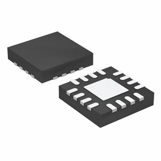
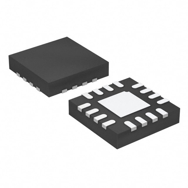
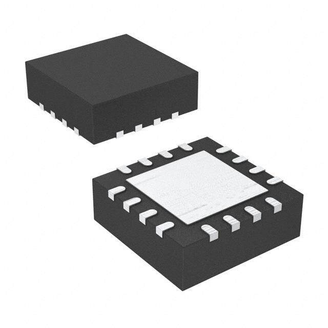
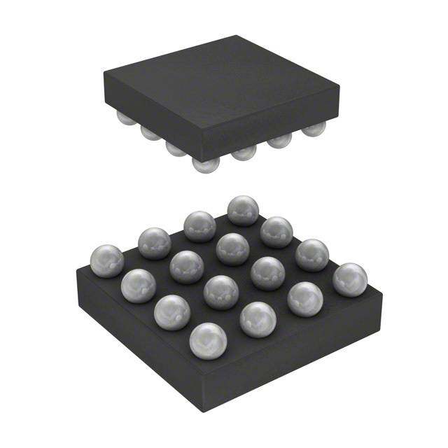
| 供应商器件封装 | 16-WQFN(3x3) |
| 其它名称 | 296-21893-1 |
| 内部驱动器 | 是 |
| 功率耗散 | 0.821 W |
| 包装 | 剪切带 (CT) |
| 商标 | Texas Instruments |
| 安装类型 | 表面贴装 |
| 安装风格 | SMD/SMT |
| 封装 | Reel |
| 封装/外壳 | 16-WFQFN 裸露焊盘 |
| 封装/箱体 | WQFN-16 |
| 工作温度 | -40°C ~ 85°C |
| 工作频率 | 750 kHz |
| 工厂包装数量 | 3000 |
| 恒压 | - |
| 恒流 | 是 |
| 拓扑 | 切换式电容器(充电泵) |
| 拓扑结构 | Boost |
| 最大工作温度 | + 85 C |
| 最大电源电流 | 6.7 mA |
| 最小工作温度 | - 40 C |
| 标准包装 | 1 |
| 电压-电源 | 3 V ~ 6 V |
| 电压-输出 | 6.5V |
| 类型 | Capacitive |
| 类型-初级 | 背光,闪灯/白光 |
| 类型-次级 | 白色 LED |
| 系列 | TPS60250 |
| 输入电压 | 3 V to 6 V |
| 输出数 | 7 |
| 输出电流 | 230 mA |
| 输出端数量 | 7 Output |
| 输出类型 | Current Mode |
| 配用 | /product-detail/zh/TPS60250EVM-185/296-31214-ND/1907934 |
| 频率 | 750kHz |
| 高电平输出电流 | 0.23 A |


- 商务部:美国ITC正式对集成电路等产品启动337调查
- 曝三星4nm工艺存在良率问题 高通将骁龙8 Gen1或转产台积电
- 太阳诱电将投资9.5亿元在常州建新厂生产MLCC 预计2023年完工
- 英特尔发布欧洲新工厂建设计划 深化IDM 2.0 战略
- 台积电先进制程称霸业界 有大客户加持明年业绩稳了
- 达到5530亿美元!SIA预计今年全球半导体销售额将创下新高
- 英特尔拟将自动驾驶子公司Mobileye上市 估值或超500亿美元
- 三星加码芯片和SET,合并消费电子和移动部门,撤换高东真等 CEO
- 三星电子宣布重大人事变动 还合并消费电子和移动部门
- 海关总署:前11个月进口集成电路产品价值2.52万亿元 增长14.8%


PDF Datasheet 数据手册内容提取
TPS60250 TPS60252 www.ti.com............................................................................................................................................................ SLVS769C–APRIL2007–REVISEDAPRIL2008 2 HIGH EFFICIENCY CHARGE PUMP FOR 7 WLEDs WITH I C INTERFACE FEATURES 1 • 3.0Vto6.0VInputVoltageRange DESCRIPTION • · 1and· 1.5ChargePump The TPS60250/2 are high efficiency, constant • FullyProgrammableCurrentwithI2C frequency charge pump DC/DC converters that use – 64DimmingStepswith25mAMaximum dual mode 1· and 1.5· conversions to maximize (SubandMainDisplayBanks) efficiency over the input voltage range. The devices – 4DimmingStepswith80mAMaximum drive up to five white LEDs for the main display and (DM5forAuxiliaryApplication) up to two white LEDs for the sub display with regulated constant current for uniform intensity. By • 2%CurrentMatchingforSubLEDsatLight utilizing adaptive 1· /1.5· charge pump modes and LoadCondition(Each100m A) very low-dropout current regulators, the TPS60250/2 • 750kHzChargePumpFrequency achieve high efficiency over the full 1-cell • Continuous230mAMaximumOutputCurrent lithium-batteryinputvoltagerange. • AutoSwitchingBetween· 1and· 1.5Modefor Four enable inputs, ENmain, ENsub1, ENsub2, and MaximumEfficiency ENaux, available through the I2C, are used for simple • Built-inSoftStartandCurrentLimit on/off controls for the independent main, sub1, sub2, and DM5 displays, respectively. To lower the • OpenLampDetection operating current when using one sub display LED, • 16-Pin3mmx3mmQFN the devices provide completely separate operation for • TPS60250(I2CSlaveAddress:1110111) thesubdisplayLEDs. • TPS60252(I2CSlaveAddress:1110110) The TPS60250/2 are available in a 16-pin 3mm x 3mmthinQFN. APPLICATIONS Main Display • CellularPhones • PDA,PMP,GPS(UpTo4InchLCDDisplay) • MultidisplayHandheldDevices 95 GND DM4 DM3 DM2 C1- DM1 90 4 Main LED - 15 mA, Sub Display VF= 3.1 V C2+ DS2 85 C2 C3 80 1mF 1mF C2- DS1 % cy - 75 C1+ VIN SCLKSDDMAT5 n cie 70 VOUT Effi 65 C4 60 4.7mF I2C Interface C1 55 4.7mF On/Off,Digital Dimming 50 3 3.5 4 4.5 5 5.5 6 Figure2.TypicalApplicationforSubandMain VI- Input Voltage - V Figure1.EfficiencyvsInputVoltage ORDERINGINFORMATION(1) PARTNUMBER PACKAGE T A TPS60250RTE 16-Pin3mm· 3mmQFN(RTE) –40(cid:176) Cto+85(cid:176) C TPS60252RTE (1) Forthemostcurrentpackageandorderinginformation,seethePackageOptionAddendumattheendofthisdocument,orseetheTI websiteatwww.ti.com. 1 Pleasebeawarethatanimportantnoticeconcerningavailability,standardwarranty,anduseincriticalapplicationsof TexasInstrumentssemiconductorproductsanddisclaimerstheretoappearsattheendofthisdatasheet. PRODUCTIONDATAinformationiscurrentasofpublicationdate. Copyright©2007–2008,TexasInstrumentsIncorporated Products conform to specifications per the terms of the Texas Instruments standard warranty. Production processing does not necessarilyincludetestingofallparameters.
TPS60250 TPS60252 SLVS769C–APRIL2007–REVISEDAPRIL2008............................................................................................................................................................ www.ti.com Thesedeviceshavelimitedbuilt-inESDprotection.Theleadsshouldbeshortedtogetherorthedeviceplacedinconductivefoam duringstorageorhandlingtopreventelectrostaticdamagetotheMOSgates. ABSOLUTE MAXIMUM RATINGS overoperatingfree-airtemperaturerange(unlessotherwisenoted)(1) VALUE UNIT V Inputvoltagerange(allpins) –0.3to7 V I MAXOutputcurrentlimit 650 mA HBMESDRating (2) 2 kV CDMESDRating(3) 500 V MMESDRating(4) 200 V T Operatingtemperaturerange –40to85 (cid:176) C A T Maximumoperatingjunctiontemperature 150 (cid:176) C J T Storagetemperature –55to150 (cid:176) C ST (1) Stressesbeyondthoselistedunderabsolutemaximumratingsmaycausepermanentdamagetothedevice.Thesearestressratings onlyandfunctionaloperationofthedeviceattheseoranyotherconditionsbeyondthoseindicatedunderrecommendedoperating conditionsisnotimplied.Exposuretoabsolute-maximum-ratedconditionsforextendedperiodsmayaffectdevicereliability. (2) TheHumanbodymodel(HBM)isa100pFcapacitordischargedthrougha1.5kΩresistorintoeachpin.Thetestingisdoneaccording JEDECsEIA/JESD22-A114. (3) ChargedDeviceModel (4) MachineModel(MM)isa200pFcapacitordischargedthrougha500nHinductorwithnoseriesresistorintoeachpin.Thetestingis doneaccordingJEDECsEIA/JESD22-A115. DISSIPATION RATINGS THERMAL THERMAL T ≤25(cid:176) CPOWER DERATINGFACTOR T =85(cid:176) CPOWER PACKAGE RESISTANCE,Rq JC RESISTANCE,Rq JA A RATING ABOVETA=25(cid:176) C A RATING QFN3· 3RTE 74.6(cid:176) C/W 48.7(cid:176) C/W 2.05W 1.13W 0.821W RECOMMENDED OPERATING CONDITIONS MIN NOM MAX UNIT V Inputvoltagerange 3.0 6.0 V I I Maximumoutputcurrent 230 mA O(max) C Inputcapacitor 4.7 m F I C Outputcapacitor 4.7 m F O C ,C Flyingcapacitor 1.0 m F 1 2 T Operatingambienttemperature –40 85 (cid:176) C A T Operatingjunctiontemperature –40 125 (cid:176) C J ELECTRICAL CHARACTERISTICS V =3.5V,T =–40(cid:176) Cto85(cid:176) C,typicalvaluesareatT =25(cid:176) C(unlessotherwisenoted) I A A PARAMETER TESTCONDITIONS MIN TYP MAX UNIT SUPPLYVOLTAGE VI Inputvoltagerange 3.0 6.0 V 750kHzSwitchingin1.5· mode IQ Operatingquiescentcurrent (IMAIN_LED=15mA· 4,IO=60mA) 6.7 mA Noswitchingin· 1mode(IO=100m A) 68 m A ISD Shutdowncurrent EnableControlRegisterhas0x00 1.3 m A VUVLO1 UVLOThresholdvoltage1(1) VIfalling 2.2 2.4 2.6 V VUVLO2 UVLOThresholdvoltage2(2) VIfalling 1.2 1.3 1.5 V (1) ShutdownchargepumpandpowerstageandkeepI2Ccontent (2) Shutdowncompletelyandcomeupwithall0'safterdevicerestart 2 SubmitDocumentationFeedback Copyright©2007–2008,TexasInstrumentsIncorporated ProductFolderLink(s):TPS60250TPS60252
TPS60250 TPS60252 www.ti.com............................................................................................................................................................ SLVS769C–APRIL2007–REVISEDAPRIL2008 ELECTRICAL CHARACTERISTICS (continued) V =3.5V,T =–40(cid:176) Cto85(cid:176) C,typicalvaluesareatT =25(cid:176) C(unlessotherwisenoted) I A A PARAMETER TESTCONDITIONS MIN TYP MAX UNIT Vhys Under-voltagelockouthysterisis UVLO1 210 mV TS Softstarttime(3) VIMIA=IN3_LEVD,C=O15=m1Am F·,4 0.5 ms CHARGEPUMP Vout Overvoltagelimit 6.5 V Fs Switchingfrequency 750 kHz · 1Mode,(VI–VO)/IO 1.2 RO Openloopoutputimpedance · 1.5Mode,(VI· 1.5–VO)/IOVI=3.0V(IO= 3.5 5.0 Ω 120mA) CURRENTSINK Km_sub Clouardrecnotnmdiatitocnh(i4n)gofsubLEDsatlight ISUB_LED=100m A· 2,VDXX=0.4V 0 ±2% Km_main LEDtoLEDCurrentmatching(5) I3M.0AINV_L≤EDV=I≤145.2mVA· 4, ±0.1% ±5% Ka Currentaccuracy ILED=15mA ±7% MainandSubDisplayCurrentRegister= ID_MS MDSax1i-m2umLEDcurrentofDM1-4and 0· 01&2(111111), 25.5 mA VDXX=0.2V ID_DM5 MaximumLEDcurrentofDM5 AuxDisplayCurrentRegister=0· 03(XXXX11) 80 mA VDropOut LEDDropoutvoltage See(6) 80 120 mV VTH_GU 1th·reMsohdoeldtvoo1lt.a5g·em(7)odetransition VloDwXeXsFtaVlDlinXXg,15mA· 4measuredonthe 85 100 120 mV VTH_GD Imnopduetvtoraltnasgietiohnysteresisfor1.5· to1· M15eamsAur·ed4asVI–(VO–VDXX_MIN),IMAIN_LED= 550 mV SERIALINTERFACETIMINGREQUIREMENTS fmax Clockfrequency 400 kHz twH(HIGH) Pulseduration,clockhightime 600 ns twL(LOW) Pulseduration,clocklowtime 1300 ns tr DATAandCLKrisetime 300 ns tf DATAandCLKfalltime 300 ns Hightime(repeated)START th(STA) condition(afterthisperiodthefirstclock 600 ns pulseisgenerated) SetuptimeforrepeatedSTART tsu(STA) condition 600 ns th(DATA) Datainputholdtime 0 ns tsu(DATA) Datainputsetuptime 100 ns tsu(STO) STOPconditionsetuptime 600 ns t(BUF) Busfreetime 1300 ns I2CCOMPATIBLEINTERFACEVOLTAGESPECIFICATION(SCLK,SDAT,VIO) VIL Low-leveIinputvoltage 3.0V≤VI≤6.0V 0 0.5 V VIH High-levelinputvoltage 3.0V≤VI≤6.0V 1.1 V VOL Low-leveloutputvoltage ILOAD=2mA 0.4 V (3) MeasurementCondition:FromenablingtheLEDdriverto90%outputvoltageafterV isalreadyup. I (4) LEDcurrentmatchingisdefinedas:(I –I )/I SUB_LED_WORST AVG_SUB AVG_SUB (5) LEDtoLEDCurrentMatchingisdefinedas:(I –I )/I MAIN_LED_WORST AVG_MAIN AVG_MAIN (6) DropoutVoltageisdefinedasV (WLEDCathode)toGNDvoltageatwhichcurrentintotheLEDdrops10%fromtheLEDcurrentat DXX V =0.2V,WLEDcurrent=15mA· 4. DXX (7) AsV drops,V eventuallyfallsbelowtheswitchoverthresholdof100mV,andTPS60250/2switchesto1.5· mode.SeetheOperating I DXX Principlesectionfordetailsaboutthemodetransitionthresholds. Copyright©2007–2008,TexasInstrumentsIncorporated SubmitDocumentationFeedback 3 ProductFolderLink(s):TPS60250TPS60252
TPS60250 TPS60252 SLVS769C–APRIL2007–REVISEDAPRIL2008............................................................................................................................................................ www.ti.com PIN ASSIGNMENTS QFN 16-PIN RTE 3mmX3mm (TOPVIEW) GND DM4 DM3 DM2 12 11 10 9 C1- DM1 13 8 C2+ 14 7 DS2 C2- 15 6 DS1 C1+ 16 5 DM5 1 2 3 4 VOUT VIN SCLK SDAT TERMINALFUNCTIONS TERMINAL I/O DESCRIPTION NAME NO. VOUT 1 O Connecttheanodesofthesub,main,andauxdisplaywhiteLEDstothispin. VIN 2 I Supplyvoltageinput.Connecttoa3Vto6Vinputsupplysource. SCLK 3 I I2CInterface SDAT 4 I/O I2CInterface DM5 5 I Currentsinkinputs.Connectthecathodeoftheauxdisplayorthe5thmaindisplaywhiteLEDtothispin. DS1 6 I Currentsinkinputs.ConnectthecathodeofoneofthesubdisplaywhiteLEDstothesepins. DS2 7 I DM1 8 I DM2 9 I Currentsinkinput.ConnectthecathodeofoneofthemaindisplaywhiteLEDstothesepins. DM3 10 I DM4 11 I GND 12 – Ground C1– 13 – ConnecttotheflyingcapacitorC1 C2+ 14 – ConnecttotheflyingcapacitorC2 C2– 15 – ConnecttotheflyingcapacitorC2 C1+ 16 – ConnecttotheflyingcapacitorC1 4 SubmitDocumentationFeedback Copyright©2007–2008,TexasInstrumentsIncorporated ProductFolderLink(s):TPS60250TPS60252
TPS60250 TPS60252 www.ti.com............................................................................................................................................................ SLVS769C–APRIL2007–REVISEDAPRIL2008 FUNCTIONAL BLOCK DIAGRAM C1+ C2- C2+ C1- VOUT DM4 DM3 DM2 DM1 16 15 14 13 1 11 10 9 8 VIN 2 1X,1.5X CHARGE PUMP GEAR CONTROL & OPEN LAMP DETECTION 7 DS2 ENold 6 DS1 I2C INTERFACE ENmain 6 Main Dimming ENsub1 ENsub2 6 Sub Dimming 5 DM5 SCLK 3 ENaux 6 AUX Dimming SDAT 4 BIAS,TEST, &MONITORING 12 GND TYPICAL CHARACTERISTICS TABLE OF GRAPHS DESCRIPTION REF EfficiencyvsInputVoltage,4MainLED-15mA,25mA Figure3 Efficiency EfficiencyvsInputVoltage,2SubLEDwithLightLoadCondition,· 1ModeOperation Figure4 SwitchResistancevsFree-AirTemperature,· 1Mode,I =230mA Figure5 LED OutputImpedanceof· 1 SwitchResistancevsFree-AirTemperature,· 1Mode,ILED=100mA Figure6 and· 1.5Mode SwitchResistancevsFree-AirTemperature,· 1.5ModeChargePumpOpen-Loop,I =230mA Figure7 LED SwitchResistancevsFree-AirTemperature,· 1.5ModeChargePumpOpen-Loop,I =100mA Figure8 LED ShutdownCurrent ShutdownCurrentvsInputVoltage Figure9 Copyright©2007–2008,TexasInstrumentsIncorporated SubmitDocumentationFeedback 5 ProductFolderLink(s):TPS60250TPS60252
TPS60250 TPS60252 SLVS769C–APRIL2007–REVISEDAPRIL2008............................................................................................................................................................ www.ti.com TYPICAL CHARACTERISTICS (continued) DESCRIPTION REF InputCurrent InputCurrentvsSupplyVoltage,4MainLED Figure10 DM5withMaximum80 DM5CurrentvsInputVoltage,Programmedwith80mA Figure11 mA CurrentAccuracy WLEDCurrentvsInputVoltage,4MainLEDwith15mA Figure12 EFFICIENCY EFFICIENCY vs vs INPUTVOLTAGE INPUTVOLTAGE (2SubLEDwithLightLoadCondition, (4MainLED-15mA,25mA) · 1ModeOperation) 100 90 25 mA, VF= 3.79 V 80 1 mA, VF= 2.8 V 80 0.5 mA, VF= 2.7 V % % Efficiency - 70 Efficiency - 60 0.2 mA, VF= 2.6 V 40 60 15 mA, VF= 3.43 V 50 20 3 4 5 6 3 4 5 6 VI- Input Voltage - V VI- Input Voltage - V Figure3. Figure4. SWITCHRESISTANCE SWITCHRESISTANCE vs vs FREE-AIRTEMPERATURE FREE-AIRTEMPERATURE (· 1Mode) (· 1Mode) 1.15 1.10 ILED= 230 mA 1.10 ILED= 100 mA VI= 3.3 V 1.05 1.05 VI= 3.3 V W 1 VI= 3.6 V Wstance - 0.951 VI= 3.6 V sistance - 00..9905 Resi 0.90 VI= 3.9 V h Re 0.85 Switch 0.85 Switc 0.80 VI= 3.9 V 0.80 0.75 0.75 0.70 0.70 0.65 -40 -20 0 20 40 60 80 -40 -20 0 20 40 60 80 TA- Free-Air Temperature - °C TA- Free-Air Temperature - °C Figure5. Figure6. 6 SubmitDocumentationFeedback Copyright©2007–2008,TexasInstrumentsIncorporated ProductFolderLink(s):TPS60250TPS60252
TPS60250 TPS60252 www.ti.com............................................................................................................................................................ SLVS769C–APRIL2007–REVISEDAPRIL2008 SWITCHRESISTANCE SWITCHRESISTANCE vs vs FREE-AIRTEMPERATURE FREE-AIRTEMPERATURE (· 1.5ModeChargePumpOpen-Loop) (· 1.5ModeChargePumpOpen-Loop) 3.8 3.8 ILED= 230 mA ILED= 100 mA 3.6 3.6 Wnce - 3.4 VI= 3 V Wnce - 3.4 VI= 3 V Resista 3.2 Resista 3.2 h h witc witc 3 S 3 S 2.8 2.8 2.6 -40 -20 0 20 40 60 80 -40 -20 0 20 40 60 80 TA- Free-Air Temperature - °C TA- Free-Air Temperature - °C Figure7. Figure8. INPUTCURRENT SHUTDOWNCURRENT vs vs SUPPLYVOLTAGE INPUTVOLTAGE (4MainLED) 10 0.16 0.15 0.14 8 0.13 A 0.12 25 mA own Current -Am 64 - Input Current - 00000.....0001198701 15 mA Shutd TA= 85°C TA= -40°C TA= 25°C ICC 000...000654 2 0.03 0.02 2 mA 0.01 0 3 4 5 6 3 4 5 6 VI- Input Voltage - V VI- Input Voltage - V Figure9. Figure10. Copyright©2007–2008,TexasInstrumentsIncorporated SubmitDocumentationFeedback 7 ProductFolderLink(s):TPS60250TPS60252
TPS60250 TPS60252 SLVS769C–APRIL2007–REVISEDAPRIL2008............................................................................................................................................................ www.ti.com DM5CURRENT WLEDCURRENT vs vs INPUTVOLTAGE INPUTVOLTAGE (Programmedwith80mA) (4MainLEDwith15mA) 0.08 0.016 IDM2 IDM3 0.07 0.06 0.4 V 0.35 V 0.3 V IDM1 IDM4 DM5 Current -A 000...000345 0.25 V0.2 V0.15 V 0.01. 0V5 V WLED Current -A 00..001142 0.02 0.01 0 0.010 2.5 3 3.5 4 3 4 5 6 VI - Input Voltage - V VI- Input Voltage - V Figure11. Figure12. 8 SubmitDocumentationFeedback Copyright©2007–2008,TexasInstrumentsIncorporated ProductFolderLink(s):TPS60250TPS60252
TPS60250 TPS60252 www.ti.com............................................................................................................................................................ SLVS769C–APRIL2007–REVISEDAPRIL2008 APPLICATION INFORMATION APPLICATION OVERVIEW Mostofthecurrenthandsetsfallintooneofthreecategories. First is the clamshell design, with a main display on the inside, a secondary display on the outside and a keypad backlight. Second is the bar design, with a main display and a keypad backlight. Third is the slide type (slide-up and slide-down) design, with a main display and two keypad banks (inside and outside). The TPS60250/2 are well suited for use in these three major phone designs because the devices have 7 individually regulated white LED current paths that drive up to five white LEDs in the main display and up to two white LEDs in sub display with regulated constant current for uniform intensity. The main and sub display LED channels drive up to 25 mA and the auxiliary LED output (DM5) that drives up to 80 mA can be assigned to keypad backlight, torch light, or low cost/weak camera flash application usingtheI2Cinterface. The TPS60250/2 circuits use only 4 external components: the input/output capacitors and 2 charge pump flying capacitors.Thefewexternalcomponentscombined with the small 3mm · 3mm QFN package provide for a small totalsolutionsize.BycombiningindependentcontrolofthreeseparatebanksofbacklightLEDswithlowcostand weak flash capability, the TPS60250/2 help designers minimize power consumption especially in the case of a lightloadconditionwhilereducingcomponentcountandpackagesize. OPERATING PRINCIPLE Charge pumps are becoming increasingly attractive in battery-operated applications where board space and maximum height of the converter are critical constraints. The major advantage of a charge pump is the use of only capacitors as storage elements. The TPS60250/2 charge pumps provide regulated LED current from a 3 V to 6 V input source. The devices operate in two modes. The 1· mode, where the input is connected to the output through a pass element, and a high efficiency 1.5· charge pump mode. The IC maximizes power efficiency by operating in 1· and 1.5· modes as input voltage and LED current conditions require. The mode of operation is automatically selected by comparing the forward voltage of the WLED plus the voltage of current sink for each LED with the input voltage. The IC starts up in 1· mode, and automatically transitions to 1.5· if the voltage at any current sink input (DM_or DS_) falls below the 100 mV transition voltage. The IC returns to 1· mode as the inputrises.Figure13providesavisualexplanationofthe1· to1.5· transition. In 1.5· mode, the internal oscillator determines the charge/discharge cycles for the flying capacitors. During a charge cycle, the flying capacitors are connected in series and charged up to the input voltage. After the on-time of the internal oscillator expires, the flying capacitors are reconfigured to be in parallel and then connected in series to the input voltage. This provides an output of 1.5· the input voltage. After the off-time of the internal oscillatorexpires,anotherchargecycleinitiatesandtheprocessrepeats. Copyright©2007–2008,TexasInstrumentsIncorporated SubmitDocumentationFeedback 9 ProductFolderLink(s):TPS60250TPS60252
TPS60250 TPS60252 SLVS769C–APRIL2007–REVISEDAPRIL2008............................................................................................................................................................ www.ti.com VA V V I O VF CPWLED Driver VDX V x1Operating I Area x1.5Operating Area VHYS VB VC Figure13.InputVoltageHysteresisBetween· 1and· 1.5Mode As shown in Figure 13, there is input hysteresis voltage between 1· and 1.5· mode to ensure stable operation duringmodetransition.Forthe1cellLi-Ionbatteryinput voltage range, the TPS6025/2 operate in 1· mode when a fully charged battery is installed. Once the battery voltage drops below the V level, which is the mode B transition voltage from 1· to 1.5· , the WLED driver operates in 1.5· mode. Once in 1.5· mode, the battery voltage must rise to the V level in order to transition from 1.5· to 1· . This hysteresis ensures stable operation C whenthereissomeinputvoltagefluctuationatthe1· /1.5· modetransition. The transition voltage, V , depends on V (the mode transition threshold voltage), V (WLED forward voltage B DX F drop)andV (thedropoutvoltageofthechargepumpstage)andiscalculatedasfollows: A V =V +V +V B A F DX V =R · I A OUT1X LEDTOTAL Where R is the 1· mode output impedance of the IC. See the Electrical Characteristics table for output OUT1X impedancespecifications. TheTPS60250/2switchupto1.5· modewhentheinputvoltageisbelowV and remain in 1.5· mode as long as B theinputislowerthanV .1.5· ModeisexitedwhentheinputvoltagerisesaboveV .V iscalculatedas: C C C V =V +550mV C F Theinputvoltagemodetransitionhysteresisvoltage(V )between1· and1.5· is calculated using the following HYS equation. V =V –V =550mV–V –V ,whereV =100mV HYS C B DX A DX Note that V is the key factor in determining V and is dependant on the 1· mode charge pump output A HYS impedanceandWLEDcurrent. 10 SubmitDocumentationFeedback Copyright©2007–2008,TexasInstrumentsIncorporated ProductFolderLink(s):TPS60250TPS60252
TPS60250 TPS60252 www.ti.com............................................................................................................................................................ SLVS769C–APRIL2007–REVISEDAPRIL2008 LED CURRENT SINKS (DM_, DS_) The TPS60250/2 have constant current sinks which drive seven individual LED current paths. Each current sink regulates the LED current to a constant value determined by the I2C interface. The internal register addressing allows the LED main channels DM1~DM5 to be controlled independently from the LED sub channels DS1~DS2. All LED channels sink up to 25 mA of current except DM5 which has an 80 mA maximum current when configuredasanauxiliaryoutput.UsingtheI2Cinterface,theusermayassignDM5tothemaindisplaybank with up to 25 mA current or as an auxiliary output for torch or keypad light or low/weak camera flash with 80 mA current. DM5 has 64 dimming steps; the same as the main and sub display banks when assigned to the main display.However,ithasitsowncurrentprogrammingregisterandenablecontrol.Whenassignedas an auxiliary, DM5has4dimmingsteps(fullscale,70%,40%,20%). These optimized current sinks minimize the voltage headroom required to drive each LED and maximize power efficiencybyincreasingtheamountoftimethecontrollerstaysin1· modebeforetransitioningto1.5· mode. OPEN LAMP DETECTION In system production it is often necessary to leave LED current paths open depending on the phone model. For example, one phone may use 2 LEDs to backlight the main display while another uses 4 LEDs. Rather than use twodifferentICsforthesedifferentphoneapplications,theTPS60250/2maybeused in both applications with no additional efficiency loss in the 2 LED applications. In traditional LED driver applications when an LED current path is open, the current sink voltage falls to ground and the current regulation circuitry drives the output to maximum voltage in an attempt to regulate the current for the missing LED path. This severely reduces system efficiency. The TPS60250/2 use 7 internal comparators to detect open lamp condition, when one or more open LED conditions occur, TPS60250/2 prevent activation of 1.5X mode transition due to missing LEDs. Open lamp detectionisenabled/disabledusingtheI2Cinterface. CAPACITOR SELECTION The TPS60250/2 are optimized to work with ceramic capacitors with a dielectric of X5R or better. The two flying capacitorsmustbethesamevaluefor proper operation. The 750 kHz switching frequency requires that the flying capacitor be less than 4.7 m F. Use of 1 m F ceramic capacitors for both charge pump flying capacitors is recommended. Forgoodinputvoltagefiltering,lowESRceramiccapacitors are recommended. A 1 m F ceramic input capacitor is sufficientformostapplications.Forbetterinputvoltagefilteringthisvaluecanbeincreasedto4.7m F. Theoutputcapacitorcontrolsthe amount of ripple on the output. Since small ripple is undetectable by the human eye, a 4.7 m F output capacitor works well. If better output filtering and lower ripple is desired, a larger output capacitormaybeused. SETTING THE LED CURRENT Figure14.DimmingStepsforSub,Main,andKeypadBacklight Figure 14 shows the dimming steps for sub, main, and auxiliary display banks in a 25 mA maximum current Copyright©2007–2008,TexasInstrumentsIncorporated SubmitDocumentationFeedback 11 ProductFolderLink(s):TPS60250TPS60252
TPS60250 TPS60252 SLVS769C–APRIL2007–REVISEDAPRIL2008............................................................................................................................................................ www.ti.com applications.Inorderto satisfy today's requirements on LED current , the TPS60250/2 cover the low LED current area from 100 m A to 1.5 mA with 100 m A dimming steps (total 16 steps for a 25 mA maximum current) for the new LCD panels which have improved transparency rates. For LED currents in the range from 2 mA to 25 mA, the devices use 48 dimming steps with 0.5 mA steps. Also, DM5 has 4 dimming steps once the current path is assignedforauxiliaryapplicationswitha80mAmaximumcurrent. SERIAL INTERFACE The serial interface is compatible with the standard and fast mode I2C specifications, allowing transfers at up to 400 kHz. The interface adds flexibility to the WLED driver solution, enabling most functions to be programmed to new values depending on the instantaneous application requirements. Register contents remain intact as long as V remainsaboveUVLO2(typical1.3V). CC For normal data transfer, DATA is allowed to change only when CLK is low. Changes when CLK is high are reserved for indicating the start and stop conditions. During data transfer, the data line must remain stable whenevertheclocklineishigh.Thereisoneclockpulseperbitofdata.Eachdata transfer is initiated with a start condition and terminated with a stop condition. When addressed, the TPS60250/2 devices generate an acknowledge bit after the reception of each byte. The master device (microprocessor) must generate an extra clock pulse that is associated with the acknowledge bit. The TPS60250/2 devices must pull down the DATA line during the acknowledge clock pulse so that the DATA line is a stable low during the high period of the acknowledge clock pulse. Setup and hold times must be taken into account. During read operations, a master must signal the end of data to the slave by not generating an acknowledge bit on the last byte that was clocked out of the slave. In this case, the slave TPS60250/2 devices must leave the data line high to enable the master togeneratethestopcondition. DATA CLK Data line Change stable; of data data valid allowed Figure15.BitTransferontheSerialInterface CE DATA CLK S P START Condition STOPCondition Figure16.STARTandSTOPConditions 12 SubmitDocumentationFeedback Copyright©2007–2008,TexasInstrumentsIncorporated ProductFolderLink(s):TPS60250TPS60252
TPS60250 TPS60252 www.ti.com............................................................................................................................................................ SLVS769C–APRIL2007–REVISEDAPRIL2008 ... ... ... SCLK ... ... ... SDAT A6 A5 A4 A0 R/W AC R7 R6 R5 R0 AC D7 D6 D5 D0 AC K K K 0 0 0 0 Start SlaveAddress RegisterAddress Data Stop NOTE:SLAVE=TPS60250 Figure17.SerialI/FREADFromTPS60250/2:ProtocolA ... ... ... ... SCLK .. .. .. .. SDAT A6 A0 R/W AC R7 R0 AC A6 A0 R/W AC D7 D0 AC K K K K 0 0 0 1 0 Start Slave Stop SlaveAddress Register SlaveAddress Drives Master Address the Data Drives NOTE:SLAVE=TPS60250 Repeated ACK and Stop Start Figure18.SerialI/FREADFromTPS60250/2:ProtocolB Figure19.SerialI/FTimingDiagram The I2C interface uses a combined protocol in which the START condition and the Slave Address are both repeated. The TPS60250 provides two I2C Slave Addresses using an internal EEPROM in case more than 1 device is used in the system. The TPS60250 primary I2C Slave Address is 1110111 and the TPS60252 primary I2CSlaveAddressis1110110.ForthealternativeI2Caddresses,contactthefactory. Copyright©2007–2008,TexasInstrumentsIncorporated SubmitDocumentationFeedback 13 ProductFolderLink(s):TPS60250TPS60252
TPS60250 TPS60252 SLVS769C–APRIL2007–REVISEDAPRIL2008............................................................................................................................................................ www.ti.com EnableControlRegister(Address:0x00h) ENABLE B7 B6 B5 B4 B3 B2 B1 B0 BITNAME X ENold ENmain ENsub2 ENsub1 ENaux DM5H DM5L Bit6 ENold(EnableOpenLampDetection) 1:OpenLampDetectionEnabled 0:OpenLampDetectionDisabled Bit5 ENmain 1:EnableMainDisplayLEDs(DM1-DM4) 0:DisableMainDisplayLEDs Bit4 ENsub2 1:EnableSubDisplayLED2(DS2) 0:DisableSubDisplayLED2 Bit3 ENsub1 1:EnableSubDisplayLED1(DS1) 0:DisableSubDisplayLED1 Bit2 ENaux 1:EnableAuxDisplayLED(DM5) 0:DisableAuxDisplayLED Bits1,0 DM5H,DM5L DM5H DM5L DM5ModeandShutdownMode (B1) (B0) 0 0 Shutdownmode.Alloutputsdisabledbutkeepregistervalues 0 1 EnabletheICandGroupDM5asmaindisplaywithmaximumcurrentof25mA 1 0 EnabletheICandsetDM5asAuxoutputwithmaximumcurrentof80mA. DimmingstepsdeterminedbyIaux0andIaux1bits. 1 1 Shutdownmode.Alloutputsdisabledbutkeepregistervalues SubDisplayCurrentControlRegister(Address:0x01h) SUBDISP B7 B6 B5 B4 B3 B2 B1 B0 CURRENT BITNAME X X Isub5 Isub4 Isub3 Isub2 Isub1 Isub0 Bits5-0 Isub5-Isub0(total64steps) 6-Bitcommand(64steps)tothesebitssetsthecurrentforDS1andDS2. ForLEDcurrentsbetween0and1.5mA,onestep=0.1mAincrement ForLEDcurrentsbetween1.5and25.5mA,onestep=0.5mAincrement MainDisplayCurrentControlRegister(Address:0x02h) MAINDISP B7 B6 B5 B4 B3 B2 B1 B0 CURRENT BITNAME X X Imain5 Imain4 Imain3 Imain2 Imain1 Imain0 Bits5-0 Imain5-Imain0(total64steps) 6-Bitcommand(64steps)tothesebitssetsthecurrentforDM1-DM4. ForLEDcurrentsbetween0and1.5mA,onestep=0.1mAincrement ForLEDcurrentsbetween1.5and25.5mA,onestep=0.5mAincrement 14 SubmitDocumentationFeedback Copyright©2007–2008,TexasInstrumentsIncorporated ProductFolderLink(s):TPS60250TPS60252
TPS60250 TPS60252 www.ti.com............................................................................................................................................................ SLVS769C–APRIL2007–REVISEDAPRIL2008 AuxOutputBrightnessandOperationModeControlRegister(Address:0x03h) AUXDISP B7 B6 B5 B4 B3 B2 B1 B0 CURRENT BITNAME Iaux5 Iaux4 Iaux3 Iaux2 Iaux1 Iaux0 Mode1 Mode0 Bits7-2(DM5settoMainDisplayMode) Iaux5-Iaux0(total64steps) 6-Bitcommand(64steps)tothesebitssetsthecurrentforDM5. ForLEDcurrentsbetween0and1.5mA,onestep=0.1mAincrement ForLEDcurrentsbetween1.5and25.5mA,onestep=0.5mAincrement Bits7-2(DM5settoAuxDisplayMode) Iaux5 Iaux4 Iaux3 Iaux2 Iaux1 Iaux0 AuxDimming (B7) (B6) (B5) (B4) (B3) (B2) Step X X X X 0 0 20% X X X X 0 1 40% X X X X 1 0 70% X X X X 1 1 100% Bits1,0 Mode1,Mode0 Mode1 Mode0 TPS60250/2Mode (B1) (B0) 0 0 Auto-SwitchoverMode.TheTPS60250/2select 1· /1.5· modeasdescribedintheOperatingPrinciple section. 0 1 1· Mode.TPS60250/2remainin1· moderegardless oftheinputvoltage.LEDcurrentmaynotregulateat lowerinputvoltageswheninthismode. 1 0 1.5· Mode.TPS60250/2remainin1.5· mode regardlessoftheinputvoltage. 1 1 Auto-SwitchoverMode.TheTPS60250/2select 1· /1.5· modeasdescribedintheOperatingPrinciple section. Copyright©2007–2008,TexasInstrumentsIncorporated SubmitDocumentationFeedback 15 ProductFolderLink(s):TPS60250TPS60252
TPS60250 TPS60252 SLVS769C–APRIL2007–REVISEDAPRIL2008............................................................................................................................................................ www.ti.com APPLICATION CIRCUITS Main Display GND DM4 DM3 DM2 C1- DM1 Sub Display C2+ DS2 C2 C3 1mF 1mF C2- DS1 C1+ DM5 VIN SCLKSDAT VOUT C4 4.7mF I2C Interface C1 On/Off,Digital Dimming 4.7mF Figure20.TheTypicalApplicationCircuitforSubandMainDisplay As shown in Figure 20, typical application circuit for a clam shell phone has 5 main LEDs and 2 sub LEDs. Recently, the LCD panel makers have developed a new panel that has an improved transparency rate which makes system efficiency with 100 m A LED current a critical load point. To meet system efficiency requirements with the light load conditions for the new LCD operating panels, the TPS60250/2 have a maximum 55 m A operatingcurrentwith100m Aoutputloadcondition.In this application, the controller always operates in 1· mode due to the WLED's low forward voltage drop (about 2.6 V with a 100 m A WLED current). Thus, the total F efficiencyatthelightloadconditionisdeterminedusingEquation1: IO(cid:1)VF (cid:1)Light(cid:3) Vin(cid:1)(cid:4)IO(cid:2)Iop(cid:5) (1) Where: I :OutputLoad(WLED)Current O V :ForwardVoltageDropofWLED F V :InputVoltage in I :OperatingCurrentofLEDDriver op 16 SubmitDocumentationFeedback Copyright©2007–2008,TexasInstrumentsIncorporated ProductFolderLink(s):TPS60250TPS60252
TPS60250 TPS60252 www.ti.com............................................................................................................................................................ SLVS769C–APRIL2007–REVISEDAPRIL2008 Main Display Auxiliary Port for Key Pad or Flash Light GND DM4 DM3 DM2 C1- DM1 C2+ DS2 C2 C3 1mF 1mF C2- DS1 C1+ DM5 Sub Display VIN SCLKSDAT VOUT C4 4.7mF I2C Interface C1 On/Off,Digital Dimming 4.7mF Figure21.TheTypicalApplicationCircuitforSub,Main,andKeypadBacklight Figure 21 shows the typical application circuit for sub, main, and keypad backlight. In this application, DM5 is assignedastheauxiliaryinputforthekeypadlightingapplication. LAYOUT GUIDELINES There are several points to consider when laying out a PCB for charge pump based solutions. In general, all capacitors should be as close as possible to the device. This is especially important when placing the flying capacitors (C2, C3 in Figure 20 and Figure 21). In cases where DM5 is assigned for torch/flash applications, with amaximum80mAWLEDcurrent,thiscurrentpathmustbekeptwidetoreducethetraceresistance. Copyright©2007–2008,TexasInstrumentsIncorporated SubmitDocumentationFeedback 17 ProductFolderLink(s):TPS60250TPS60252
TPS60250 TPS60252 SLVS769C–APRIL2007–REVISEDAPRIL2008............................................................................................................................................................ www.ti.com Revision History ChangesfromRevisionB(November2007)toRevisionC ........................................................................................... Page • AddedTPS60252deviceinformation.................................................................................................................................... 1 18 SubmitDocumentationFeedback Copyright©2007–2008,TexasInstrumentsIncorporated ProductFolderLink(s):TPS60250TPS60252
PACKAGE OPTION ADDENDUM www.ti.com 6-Feb-2020 PACKAGING INFORMATION Orderable Device Status Package Type Package Pins Package Eco Plan Lead/Ball Finish MSL Peak Temp Op Temp (°C) Device Marking Samples (1) Drawing Qty (2) (6) (3) (4/5) TPS60250RTER ACTIVE WQFN RTE 16 3000 Green (RoHS NIPDAU Level-2-260C-1 YEAR -40 to 85 BSR & no Sb/Br) TPS60250RTET ACTIVE WQFN RTE 16 250 Green (RoHS NIPDAU Level-2-260C-1 YEAR -40 to 85 BSR & no Sb/Br) TPS60252RTER ACTIVE WQFN RTE 16 3000 Green (RoHS NIPDAU Level-2-260C-1 YEAR -40 to 85 CFN & no Sb/Br) TPS60252RTET ACTIVE WQFN RTE 16 250 Green (RoHS NIPDAU Level-2-260C-1 YEAR -40 to 85 CFN & no Sb/Br) (1) The marketing status values are defined as follows: ACTIVE: Product device recommended for new designs. LIFEBUY: TI has announced that the device will be discontinued, and a lifetime-buy period is in effect. NRND: Not recommended for new designs. Device is in production to support existing customers, but TI does not recommend using this part in a new design. PREVIEW: Device has been announced but is not in production. Samples may or may not be available. OBSOLETE: TI has discontinued the production of the device. (2) RoHS: TI defines "RoHS" to mean semiconductor products that are compliant with the current EU RoHS requirements for all 10 RoHS substances, including the requirement that RoHS substance do not exceed 0.1% by weight in homogeneous materials. Where designed to be soldered at high temperatures, "RoHS" products are suitable for use in specified lead-free processes. TI may reference these types of products as "Pb-Free". RoHS Exempt: TI defines "RoHS Exempt" to mean products that contain lead but are compliant with EU RoHS pursuant to a specific EU RoHS exemption. Green: TI defines "Green" to mean the content of Chlorine (Cl) and Bromine (Br) based flame retardants meet JS709B low halogen requirements of <=1000ppm threshold. Antimony trioxide based flame retardants must also meet the <=1000ppm threshold requirement. (3) MSL, Peak Temp. - The Moisture Sensitivity Level rating according to the JEDEC industry standard classifications, and peak solder temperature. (4) There may be additional marking, which relates to the logo, the lot trace code information, or the environmental category on the device. (5) Multiple Device Markings will be inside parentheses. Only one Device Marking contained in parentheses and separated by a "~" will appear on a device. If a line is indented then it is a continuation of the previous line and the two combined represent the entire Device Marking for that device. (6) Lead/Ball Finish - Orderable Devices may have multiple material finish options. Finish options are separated by a vertical ruled line. Lead/Ball Finish values may wrap to two lines if the finish value exceeds the maximum column width. Important Information and Disclaimer:The information provided on this page represents TI's knowledge and belief as of the date that it is provided. TI bases its knowledge and belief on information provided by third parties, and makes no representation or warranty as to the accuracy of such information. Efforts are underway to better integrate information from third parties. TI has taken and Addendum-Page 1
PACKAGE OPTION ADDENDUM www.ti.com 6-Feb-2020 continues to take reasonable steps to provide representative and accurate information but may not have conducted destructive testing or chemical analysis on incoming materials and chemicals. TI and TI suppliers consider certain information to be proprietary, and thus CAS numbers and other limited information may not be available for release. In no event shall TI's liability arising out of such information exceed the total purchase price of the TI part(s) at issue in this document sold by TI to Customer on an annual basis. Addendum-Page 2
PACKAGE MATERIALS INFORMATION www.ti.com 14-Jul-2012 TAPE AND REEL INFORMATION *Alldimensionsarenominal Device Package Package Pins SPQ Reel Reel A0 B0 K0 P1 W Pin1 Type Drawing Diameter Width (mm) (mm) (mm) (mm) (mm) Quadrant (mm) W1(mm) TPS60250RTER WQFN RTE 16 3000 330.0 12.4 3.3 3.3 1.1 8.0 12.0 Q2 TPS60250RTET WQFN RTE 16 250 180.0 12.4 3.3 3.3 1.1 8.0 12.0 Q2 TPS60252RTER WQFN RTE 16 3000 330.0 12.4 3.3 3.3 1.1 8.0 12.0 Q2 TPS60252RTET WQFN RTE 16 250 180.0 12.4 3.3 3.3 1.1 8.0 12.0 Q2 PackMaterials-Page1
PACKAGE MATERIALS INFORMATION www.ti.com 14-Jul-2012 *Alldimensionsarenominal Device PackageType PackageDrawing Pins SPQ Length(mm) Width(mm) Height(mm) TPS60250RTER WQFN RTE 16 3000 367.0 367.0 35.0 TPS60250RTET WQFN RTE 16 250 210.0 185.0 35.0 TPS60252RTER WQFN RTE 16 3000 367.0 367.0 35.0 TPS60252RTET WQFN RTE 16 250 210.0 185.0 35.0 PackMaterials-Page2
None
None
None
IMPORTANTNOTICEANDDISCLAIMER TI PROVIDES TECHNICAL AND RELIABILITY DATA (INCLUDING DATASHEETS), DESIGN RESOURCES (INCLUDING REFERENCE DESIGNS), APPLICATION OR OTHER DESIGN ADVICE, WEB TOOLS, SAFETY INFORMATION, AND OTHER RESOURCES “AS IS” AND WITH ALL FAULTS, AND DISCLAIMS ALL WARRANTIES, EXPRESS AND IMPLIED, INCLUDING WITHOUT LIMITATION ANY IMPLIED WARRANTIES OF MERCHANTABILITY, FITNESS FOR A PARTICULAR PURPOSE OR NON-INFRINGEMENT OF THIRD PARTY INTELLECTUAL PROPERTY RIGHTS. These resources are intended for skilled developers designing with TI products. You are solely responsible for (1) selecting the appropriate TI products for your application, (2) designing, validating and testing your application, and (3) ensuring your application meets applicable standards, and any other safety, security, or other requirements. These resources are subject to change without notice. TI grants you permission to use these resources only for development of an application that uses the TI products described in the resource. Other reproduction and display of these resources is prohibited. No license is granted to any other TI intellectual property right or to any third party intellectual property right. TI disclaims responsibility for, and you will fully indemnify TI and its representatives against, any claims, damages, costs, losses, and liabilities arising out of your use of these resources. TI’s products are provided subject to TI’s Terms of Sale (www.ti.com/legal/termsofsale.html) or other applicable terms available either on ti.com or provided in conjunction with such TI products. TI’s provision of these resources does not expand or otherwise alter TI’s applicable warranties or warranty disclaimers for TI products. Mailing Address: Texas Instruments, Post Office Box 655303, Dallas, Texas 75265 Copyright © 2020, Texas Instruments Incorporated