ICGOO在线商城 > 集成电路(IC) > PMIC - 栅极驱动器 > LM5101CMYE/NOPB

 Datasheet下载
- 型号: LM5101CMYE/NOPB
- 制造商: Texas Instruments
- 库位|库存: xxxx|xxxx
- 要求:
| 数量阶梯 | 香港交货 | 国内含税 |
| +xxxx | $xxxx | ¥xxxx |
查看当月历史价格
查看今年历史价格
LM5101CMYE/NOPB产品简介:
ICGOO电子元器件商城为您提供LM5101CMYE/NOPB由Texas Instruments设计生产,在icgoo商城现货销售,并且可以通过原厂、代理商等渠道进行代购。 LM5101CMYE/NOPB价格参考¥8.10-¥16.60。Texas InstrumentsLM5101CMYE/NOPB封装/规格:PMIC - 栅极驱动器, Half-Bridge Gate Driver IC Non-Inverting 8-MSOP-EP。您可以下载LM5101CMYE/NOPB参考资料、Datasheet数据手册功能说明书,资料中有LM5101CMYE/NOPB 详细功能的应用电路图电压和使用方法及教程。
| 参数 | 数值 |
| 产品目录 | 集成电路 (IC)半导体 |
| 描述 | IC DVR HALF-BRDG 100V 1A 8-EMSOP门驱动器 100V 1A Half-Bridge Driver |
| 产品分类 | PMIC - MOSFET,电桥驱动器 - 外部开关集成电路 - IC |
| 品牌 | Texas Instruments |
| 产品手册 | http://www.ti.com/lit/gpn/lm5101c |
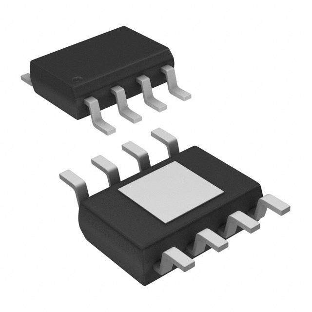
| 产品图片 |
|
| rohs | 符合RoHS无铅 / 符合限制有害物质指令(RoHS)规范要求 |
| 产品系列 | 电源管理 IC,门驱动器,Texas Instruments LM5101CMYE/NOPB- |
| 数据手册 | |
| 产品型号 | LM5101CMYE/NOPB |
| PCN设计/规格 | |
| 上升时间 | 990 ns (Typ) |
| 下降时间 | 715 ns (Typ) |
| 产品目录页面 | |
| 产品种类 | 门驱动器 |
| 供应商器件封装 | 8-MSOP-EP |
| 其它名称 | *LM5101CMYE/NOPB |
| 包装 | 剪切带 (CT) |
| 商标 | Texas Instruments |
| 安装类型 | 表面贴装 |
| 安装风格 | SMD/SMT |
| 封装 | Reel |
| 封装/外壳 | 8-TSSOP,8-MSOP(0.118",3.00mm 宽)裸焊盘 |
| 封装/箱体 | MSOP |
| 工作温度 | -40°C ~ 125°C |
| 工厂包装数量 | 250 |
| 延迟时间 | 26ns |
| 最大关闭延迟时间 | 4 ns (Typ) |
| 最大工作温度 | + 125 C |
| 最大开启延迟时间 | 4 ns (Typ) |
| 最小工作温度 | - 40 C |
| 标准包装 | 1 |
| 激励器数量 | 2 Driver |
| 电压-电源 | 9 V ~ 14 V |
| 电流-峰值 | 1A |
| 电源电压-最大 | 14 V |
| 电源电压-最小 | 9 V |
| 电源电流 | 2 mA (Typ) |
| 类型 | High and Low Side |
| 系列 | LM5101C |
| 输入类型 | 非反相 |
| 输出数 | 2 |
| 输出电流 | 1 A (Typ) |
| 输出端数量 | 2 |
| 配置 | Non-Inverting |
| 配置数 | 1 |
| 高压侧电压-最大值(自举) | 118V |


- 商务部:美国ITC正式对集成电路等产品启动337调查
- 曝三星4nm工艺存在良率问题 高通将骁龙8 Gen1或转产台积电
- 太阳诱电将投资9.5亿元在常州建新厂生产MLCC 预计2023年完工
- 英特尔发布欧洲新工厂建设计划 深化IDM 2.0 战略
- 台积电先进制程称霸业界 有大客户加持明年业绩稳了
- 达到5530亿美元!SIA预计今年全球半导体销售额将创下新高
- 英特尔拟将自动驾驶子公司Mobileye上市 估值或超500亿美元
- 三星加码芯片和SET,合并消费电子和移动部门,撤换高东真等 CEO
- 三星电子宣布重大人事变动 还合并消费电子和移动部门
- 海关总署:前11个月进口集成电路产品价值2.52万亿元 增长14.8%


PDF Datasheet 数据手册内容提取
Product Sample & Technical Tools & Support & Folder Buy Documents Software Community LM5100A,LM5100B,LM5100C LM5101A,LM5101B,LM5101C SNOSAW2Q–SEPTEMBER2006–REVISEDNOVEMBER2015 LM5100A/B/C, LM5101A/B/C 3-A, 2-A, and 1-A High-Voltage, High-Side and Low-Side Gate Drivers 1 Features An integrated high-voltage diode is provided to charge the high-side gate drive bootstrap capacitor. A • DrivesBothaHigh-SideandLow-SideN-Channel 1 robust level shifter operates at high speed while MOSFETs consuming low power and providing clean level • IndependentHigh-andLow-DriverLogicInputs transitions from the control logic to the high-side gate • BootstrapSupplyVoltageupto118VDC driver. Undervoltage lockout is provided on both the low-side and the high-side power rails. These devices • FastPropagationTimes(25-nsTypical) are available in the standard SOIC-8 pin, SO • Drives1000-pFLoadWith8-nsRiseandFall PowerPAD-8 pin, and the WSON-10 pin packages. Times The LM5100C and LM5101C are also available in • ExcellentPropagationDelayMatching(3-ns MSOP-PowerPAD-8 package. The LM5101A is also availableinWSON-8pinpackage. Typical) • SupplyRailUndervoltageLockout DeviceInformation(1) • LowPowerConsumption PEAKOUTPUT PARTNUMBER INPUTTHRESHOLD • PinCompatibleWithHIP2100/HIP2101 CURRENT LM5100A CMOS 3A 2 Applications LM5101A TTL 3A • Current-FedPush-PullConverters LM5100B CMOS 2A • HalfandFullBridgePowerConverters LM5101B TTL 2A • SynchronousBuckConverters LM5100C CMOS 1A LM5101C TTL 1A • TwoSwitchForwardPowerConverters • ForwardwithActiveClampConverters (1) For all available packages, see the orderable addendum at theendofthedatasheet. 3 Description The LM5100A/B/C and LM5101A/B/C high-voltage gate drivers are designed to drive both the high-side and the low-side N-Channel MOSFETs in a synchronous buck or a half-bridge configuration. The floating high-side driver is capable of operating with supply voltages up to 100 V. The A versions provide a full 3-A of gate drive, while the B and C versions provide 2 A and 1 A, respectively. The outputs are independently controlled with CMOS input thresholds (LM5100A/B/C)orTTLinputthresholds (LM5101A/B/C). SimplifiedBlockDiagram HB UVLO HO LEVEL DRIVER SHIFT HS HI VDD UVLO LO LI DRIVER GND 1 An IMPORTANT NOTICE at the end of this data sheet addresses availability, warranty, changes, use in safety-critical applications, intellectualpropertymattersandotherimportantdisclaimers.PRODUCTIONDATA.
LM5100A,LM5100B,LM5100C LM5101A,LM5101B,LM5101C SNOSAW2Q–SEPTEMBER2006–REVISEDNOVEMBER2015 www.ti.com Table of Contents 1 Features.................................................................. 1 8.3 FeatureDescription.................................................14 2 Applications........................................................... 1 8.4 DeviceFunctionalModes........................................15 3 Description............................................................. 1 9 ApplicationandImplementation........................ 16 4 RevisionHistory..................................................... 2 9.1 ApplicationInformation............................................16 9.2 TypicalApplication .................................................16 5 DeviceComparisonTable..................................... 3 10 PowerSupplyRecommendations..................... 20 6 PinConfigurationandFunctions......................... 3 11 Layout................................................................... 21 7 Specifications......................................................... 5 11.1 LayoutGuidelines.................................................21 7.1 AbsoluteMaximumRatings .....................................5 11.2 LayoutExample....................................................21 7.2 ESDRatings..............................................................5 12 DeviceandDocumentationSupport................. 22 7.3 RecommendedOperatingConditions.......................5 7.4 ThermalInformation..................................................6 12.1 DocumentationSupport .......................................22 7.5 ElectricalCharacteristics.........................................6 12.2 RelatedLinks........................................................22 7.6 SwitchingCharacteristics.........................................8 12.3 CommunityResources..........................................22 7.7 TypicalCharacteristics............................................10 12.4 Trademarks...........................................................22 12.5 ElectrostaticDischargeCaution............................22 8 DetailedDescription............................................ 14 12.6 Glossary................................................................22 8.1 Overview.................................................................14 13 Mechanical,Packaging,andOrderable 8.2 FunctionalBlockDiagram.......................................14 Information........................................................... 22 4 Revision History NOTE:Pagenumbersforpreviousrevisionsmaydifferfrompagenumbersinthecurrentversion. ChangesfromRevisionP(March2013)toRevisionQ Page • AddedESDRatingstable,ThermalInformationtable,FeatureDescriptionsection,DeviceFunctionalModes, ApplicationandImplementationsection,PowerSupplyRecommendationssection,Layoutsection,Deviceand DocumentationSupportsection,andMechanical,Packaging,andOrderableInformationsection. .................................... 1 ChangesfromRevisionO(March2013)toRevisionP Page • ChangedlayoutofNationalDataSheettoTIformat........................................................................................................... 19 2 SubmitDocumentationFeedback Copyright©2006–2015,TexasInstrumentsIncorporated ProductFolderLinks:LM5100A LM5100B LM5100CLM5101A LM5101B LM5101C
LM5100A,LM5100B,LM5100C LM5101A,LM5101B,LM5101C www.ti.com SNOSAW2Q–SEPTEMBER2006–REVISEDNOVEMBER2015 5 Device Comparison Table PARTNUMBER PACKAGE BODYSIZE(NOM) WSON(10) 4.00mm×4.00mm LM5100A,LM5100C SOPowerPAD™(8) 3.90mm×4.89mm SOIC(8) 3.91mm×4.90mm WSON(10) 4.00mm×4.00mm LM5100B,LM5101B SOIC(8) 3.91mm×4.90mm WSON(8) 4.00mm×4.00mm WSON(10) 4.00mm×4.00mm LM5101A SOPowerPAD(8) 3.90mm×4.89mm SOIC(8) 3.91mm×4.90mm MSOPPowerPAD(8) 3.00mm×3.00mm LM5101C WSON(10) 4.00mm×4.00mm SOIC(8) 3.91mm×4.90mm 6 Pin Configuration and Functions DPackage 8-PinSOIC DPRPackage TopView 10-PinWSONWithExposedThermalPad TopView VDD 1 8 LO VDD 1 10 LO HB 2 7 VSS HB 2 9 VSS SOIC-8 HO 3 6 LI HO 3 WSON-10 8 LI HS 4 7 HI HS 4 5 HI NC 5 6 NC NGTPackage 8-PinWSONWithExposedThermalPad DDAPackage TopView 8-PinSOPowerPAD TopView VDD 1 8 LO VDD 1 8 LO HB 2 7 VSS WSON-8 HO 3 6 LI HB 2 7 VSS SO PowerPad-8 HS 4 5 HI HO 3 6 LI HS 4 5 HI Exposed Pad Connect to VSS Copyright©2006–2015,TexasInstrumentsIncorporated SubmitDocumentationFeedback 3 ProductFolderLinks:LM5100A LM5100B LM5100CLM5101A LM5101B LM5101C
LM5100A,LM5100B,LM5100C LM5101A,LM5101B,LM5101C SNOSAW2Q–SEPTEMBER2006–REVISEDNOVEMBER2015 www.ti.com DGNPackage 8-PinMSOP-PowerPAD TopView VDD 1 8 LO HB 2 7 VSS MSOP- PowerPad-8 HO 3 6 LI HS 4 5 HI PinFunctions PIN I/O DESCRIPTION NAME 8PINS 10PINS(1) High-sidegatedriverbootstrapsupply.Connectthepositiveterminalofthebootstrap HB 2 2 I capacitortoHBandthenegativeterminaltoHS.Thebootstrapcapacitorshouldbe placedasclosetotheICaspossible. High-sidedrivercontrolinput.TheLM5100A/B/CinputshaveCMOStypethresholds. HI 5 7 I TheLM5101A/B/CinputshaveTTLtypethresholds.Unusedinputsshouldbetiedto groundandnotleftopen. High-sidegatedriveroutput.Connecttothegateofhigh-sideMOSFETwithashort, HO 3 3 O lowinductancepath. High-sideMOSFETsourceconnection.Connecttothebootstrapcapacitornegative HS 4 4 — terminalandthesourceofthehigh-sideMOSFET. Low-sidedrivercontrolinput.TheLM5100A/B/CinputshaveCMOStypethresholds. LI 6 8 I TheLM5101A/B/CinputshaveTTLtypethresholds.Unusedinputsshouldbetiedto groundandnotleftopen. Low-sidegatedriveroutput.Connecttothegateofthelow-sideMOSFETwitha LO 8 10 O short,lowinductancepath. Positivegatedrivesupply.LocallydecoupletoVSSusinglowESR/ESLcapacitor VDD 1 1 I locatedasclosetotheICaspossible. VSS 7 9 — Groundreturn.Allsignalsarereferencedtothisground. TIrecommendsthattheexposedpadonthebottomofthepackageissolderedto EP(2) — groundplaneonthePCboard,andthatgroundplaneshouldextendoutfrom beneaththeICtohelpdissipateheat. (1) ForWSON-10package,pins5and6havenoconnection. (2) Exposedpadisnotavailableonthe8-pinSOICpackage. 4 SubmitDocumentationFeedback Copyright©2006–2015,TexasInstrumentsIncorporated ProductFolderLinks:LM5100A LM5100B LM5100CLM5101A LM5101B LM5101C
LM5100A,LM5100B,LM5100C LM5101A,LM5101B,LM5101C www.ti.com SNOSAW2Q–SEPTEMBER2006–REVISEDNOVEMBER2015 7 Specifications 7.1 Absolute Maximum Ratings See (1)(2) MIN MAX UNIT VDDtoVSS −0.3 18 V HBtoHS −0.3 18 V LIorHIinput −0.3 V +0.3 V DD LOoutput −0.3 V +0.3 V DD HOoutput V −0.3 V +0.3 V HS HB HStoVSS (3) −5 100 V HBtoVSS 118 V Junctiontemperature 150 °C Storagetemperature −55 150 °C (1) StressesbeyondthoselistedunderAbsoluteMaximumRatingsmaycausepermanentdamagetothedevice.Thesearestressratings only,whichdonotimplyfunctionaloperationofthedeviceattheseoranyotherconditionsbeyondthoseindicatedunderRecommended OperatingConditions.Exposuretoabsolute-maximum-ratedconditionsforextendedperiodsmayaffectdevicereliability. (2) IfMilitaryorAerospacespecifieddevicesarerequired,contacttheTexasInstrumentsSalesOfficeorDistributorsforavailabilityand specifications. (3) IntheapplicationtheHSnodeisclampedbythebodydiodeoftheexternallowerN-MOSFET,thereforetheHSnodewillgenerallynot exceed–1V.However,insomeapplications,boardresistanceandinductancemayresultintheHSnodeexceedingthisstatedvoltage transiently.Ifnegativetransientsoccur,theHSvoltagemustneverbemorenegativethanVDD–15V.ForexampleifVDD=10V,the negativetransientsatHSmustnotexceed–5V. 7.2 ESD Ratings VALUE UNIT Human-bodymodel(HBM),perANSI/ESDA/JEDECJS-001(1) ±2000 Electrostatic V OptionA 50 V (ESD) discharge MachineModel(MM) (2) OptionBandC 100 (1) TheHumanBodyModel(HBM)isa100-pFcapacitordischargedthrougha1.5-kΩresistorintoeachpin.2kVforallpinsexceptPin2, Pin3andPin4whichareratedat1000VforHBM. (2) MachineModel(MM)ratingsare:100V(MM)forOptionsBandC;50V(MM)forOptionA. 7.3 Recommended Operating Conditions MIN NOM MAX UNIT VDD 9 14 V HS –1 100 V HB V +8 V +14 V HS HS HSslewrate <50 V/ns Junctiontemperature −40 125 °C Copyright©2006–2015,TexasInstrumentsIncorporated SubmitDocumentationFeedback 5 ProductFolderLinks:LM5100A LM5100B LM5100CLM5101A LM5101B LM5101C
LM5100A,LM5100B,LM5100C LM5101A,LM5101B,LM5101C SNOSAW2Q–SEPTEMBER2006–REVISEDNOVEMBER2015 www.ti.com 7.4 Thermal Information LM5100A, LM5100x, LM5100C, LM5101C LM5101A LM5101x LM5101A THERMALMETRIC(1) UNIT SOPowerPAD PowMeSrOPAP-D(2) WSON(2) WSON(2) SOIC 8PINS 8PINS 8PINS 10PINS 8PINS R Junction-to-ambientthermalresistance(3) 40 80 37.8 40 170 °C/W θJA R Junction-to-case(top)thermalresistance — — 36.7 — — °C/W θJC(top) R Junction-to-boardthermalresistance — — 14.9 — — °C/W θJB ψ Junction-to-topcharacterizationparameter — — 0.3 — — °C/W JT ψ Junction-to-boardcharacterizationparameter — — 15.2 — — °C/W JB R Junction-to-case(bottom)thermalresistance — — 4.4 — — °C/W θJC(bot) (1) Formoreinformationabouttraditionalandnewthermalmetrics,seetheSemiconductorandICPackageThermalMetricsapplication report,SPRA953. (2) 4-layerboardwithCufinishedthickness1.5,1,1,1.5oz.Maximumdiesizeused.5×bodylengthofCutraceonPCBtop. 50-mm×50-mmgroundandpowerplanesembeddedinPCB.SeeApplicationNoteAN-1187(SNOA401). (3) TheR isnotagivenconstantforthepackageanddependsontheprintedcircuitboarddesignandtheoperatingenvironment. θJA 7.5 Electrical Characteristics unlessotherwisespecified,limitsareforT =25°C,V =V =12V,V =V =0V,noloadonLOorHO (1). J DD HB SS HS PARAMETER TESTCONDITIONS MIN TYP MAX UNIT SUPPLYCURRENTS VDDquiescentcurrent, TJ=25°C 0.1 LI=HI=0V mA LM5100A/B/C T =–40°Cto125°C 0.2 J I DD VDDquiescentcurrent, TJ=25°C 0.25 LI=HI=0V mA LM5101A/B/C T =–40°Cto125°C 0.4 J T =25°C 2 J I VDDoperatingcurrent f=500kHz mA DDO T =–40°Cto125°C 3 J T =25°C 0.06 J I TotalHBquiescentcurrent LI=HI=0V mA HB T =–40°Cto125°C 0.2 J T =25°C 1.6 J I TotalHBoperatingcurrent f=500kHz mA HBO T =–40°Cto125°C 3 J T =25°C 0.1 J I HBtoVSScurrent,quiescent HS=HB=100V µA HBS T =–40°Cto125°C 10 J I HBtoVSScurrent,operating f=500kHz 0.4 mA HBSO INPUTPINS Inputvoltagethreshold TJ=25°C 5.4 V RisingEdge V IL LM5100A/B/C T =–40°Cto125°C 4.5 6.3 J Inputvoltagethreshold TJ=25°C 1.8 V RisingEdge V IL LM5101A/B/C T =–40°Cto125°C 1.3 2.3 J Inputvoltagehysteresis V 500 mV IHYS LM5100A/B/C Inputvoltagehysteresis V 50 mV IHYS LM5101A/B/C T =25°C 200 J R Inputpulldownresistance kΩ I T =–40°Cto125°C 100 400 J (1) Minimumandmaximumlimitsare100%productiontestedat25°C.Limitsovertheoperatingtemperaturerangearespecifiedthrough correlationusingStatisticalQualityControl(SQC)methods.LimitsareusedtocalculateAverageOutgoingQualityLevel(AOQL). 6 SubmitDocumentationFeedback Copyright©2006–2015,TexasInstrumentsIncorporated ProductFolderLinks:LM5100A LM5100B LM5100CLM5101A LM5101B LM5101C
LM5100A,LM5100B,LM5100C LM5101A,LM5101B,LM5101C www.ti.com SNOSAW2Q–SEPTEMBER2006–REVISEDNOVEMBER2015 Electrical Characteristics (continued) unlessotherwisespecified,limitsareforT =25°C,V =V =12V,V =V =0V,noloadonLOorHO(1). J DD HB SS HS PARAMETER TESTCONDITIONS MIN TYP MAX UNIT UNDERVOLTAGEPROTECTION T =25°C 6.9 J V VDDrisingthreshold V DDR T =–40°Cto125°C 6 7.4 J V VDDthresholdhysteresis 0.5 V DDH T =25°C 6.6 J V HBrisingthreshold V HBR T =–40°Cto125°C 5.7 7.1 J V HBthresholdhysteresis 0.4 V HBH BOOTSTRAPDIODE T =25°C 0.52 J V Low-currentforwardvoltage I =100µA V DL VDD-HB T =–40°Cto125°C 0.85 J T =25°C 0.8 J V High-currentforwardvoltage I =100mA V DH VDD-HB T =–40°Cto125°C 1 J Dynamicresistance TJ=25°C 1.0 R I =100mA Ω D LM5100A/B/C,LM5101A/B/C VDD-HB T =–40°Cto125°C 1.65 J LOANDHOGATEDRIVER Low-leveloutputvoltage TJ=25°C 0.12 V LM5100A/LM5101A T =–40°Cto125°C 0.25 J Low-leveloutputvoltage TJ=25°C 0.16 V I =I =100mA V OL LM5100B/LM5101B HO LO T =–40°Cto125°C 0.4 J Low-leveloutputvoltage TJ=25°C 0.28 V LM5100C/LM5101C T =–40°Cto125°C 0.65 J High-leveloutputvoltage TJ=25°C 0.24 V LM5100A/LM5101A T =–40°Cto125°C 0.45 J High-leveloutputvoltage IHO=ILO=100mA TJ=25°C 0.28 V V =VDD–LOor V OH LM5100B/LM5101B VOOHH=HB-HO TJ=–40°Cto125°C 0.60 High-leveloutputvoltage TJ=25°C 0.6 V LM5100C/LM5101C T =–40°Cto125°C 1.10 J Peakpullupcurrent 3 A LM5100A/LM5101A Peakpullupcurrent I HO,LO=0V T =25°C 2 A OHL LM5100B/LM5101B J Peakpullupcurrent 1 A LM5100C/LM5101C Peakpulldowncurrent 3 A LM5100A/LM5101A Peakpulldowncurrent I HO,LO=12V T =25°C 2 A OLL LM5100B/LM5101B J Peakpulldowncurrent 1 A LM5100C/LM5101C Copyright©2006–2015,TexasInstrumentsIncorporated SubmitDocumentationFeedback 7 ProductFolderLinks:LM5100A LM5100B LM5100CLM5101A LM5101B LM5101C
LM5100A,LM5100B,LM5100C LM5101A,LM5101B,LM5101C SNOSAW2Q–SEPTEMBER2006–REVISEDNOVEMBER2015 www.ti.com 7.6 Switching Characteristics LimitsinstandardtypeareforT =25°Conly;limitsinboldfacetypeapplyoverthejunctiontemperature(T)rangeof–40°C J J to+125°C.MinimumandMaximumlimitsarespecifiedthroughtest,design,orstatisticalcorrelation.Typicalvaluesrepresent themostlikelyparametricnormatT =25°C,andareprovidedforreferencepurposesonly.Unlessotherwisespecified,V = J DD V =12V,V =V =0V,NoLoadonLOorHO (1). HB SS HS PARAMETER TESTCONDITIONS MIN TYP MAX UNIT LOturnoffpropagationdelayLM5100A/B/C 20 45 ns t LIFallingtoLOFalling LPHL LOturnoffpropagationdelayLM5101A/B/C 22 56 ns LOturnonpropagationdelayLM5100A/B/C 20 45 ns t LIRisingtoLORising LPLH LOturnonpropagationdelayLM5101A/B/C 26 56 ns HOturnoffpropagationdelay 20 45 ns LM5100A/B/C t HIFallingtoHOFalling HPHL HOturnoffpropagationdelay 22 56 ns LM5101A/B/C LOturnonpropagationdelayLM5100A/B/C 20 45 ns t HIRisingtoHORising HPLH LOturnonpropagationdelayLM5101A/B/C 26 56 ns Delaymatching:LOonandHOoff 1 10 ns LM5100A/B/C t MON Delaymatching:LOonandHOoff 4 10 ns LM5101A/B/C Delaymatching:LOoffandHOon 1 10 ns LM5100A/B/C t MOFF Delaymatching:LOonandHOoff 4 10 ns LM5101A/B/C t ,t Eitheroutputriseandfalltime C =1000pF 8 ns RC FC L Outputrisetime(3Vto9V) 430 ns LM5100A/LM5101A Outputrisetime(3Vto9V) t C =0.1µF 570 ns R LM5100B/LM5101B L Outputrisetime(3Vto9V) 990 ns LM5100C/LM5101C Outputfalltime(3Vto9V) 260 ns LM5100A/LM5101A Outputfalltime(3Vto9V) t C =0.1µF 430 ns F LM5100B/LM5101B L Outputfalltime(3Vto9V) 715 ns LM5100C/LM5101C Minimuminputpulsewidththatchanges t 50 ns PW theoutput I =100mA, t Bootstrapdiodereverserecoverytime F 37 ns BS I =100mA R (1) Minimumandmaximumlimitsare100%productiontestedat25°C.Limitsovertheoperatingtemperaturerangearespecifiedthrough correlationusingStatisticalQualityControl(SQC)methods.LimitsareusedtocalculateAverageOutgoingQualityLevel(AOQL). 8 SubmitDocumentationFeedback Copyright©2006–2015,TexasInstrumentsIncorporated ProductFolderLinks:LM5100A LM5100B LM5100CLM5101A LM5101B LM5101C
LM5100A,LM5100B,LM5100C LM5101A,LM5101B,LM5101C www.ti.com SNOSAW2Q–SEPTEMBER2006–REVISEDNOVEMBER2015 LI LI HI HI tHPLH tLPLH tHPHL tLPHL LO LO HO HO tMON tMOFF Figure1. TimingDiagram Copyright©2006–2015,TexasInstrumentsIncorporated SubmitDocumentationFeedback 9 ProductFolderLinks:LM5100A LM5100B LM5100CLM5101A LM5101B LM5101C
LM5100A,LM5100B,LM5100C LM5101A,LM5101B,LM5101C SNOSAW2Q–SEPTEMBER2006–REVISEDNOVEMBER2015 www.ti.com 7.7 Typical Characteristics 5.0 5.0 4.5 4.5 4.0 4.0 3.5 LM5100A/LM5101A 3.5 LM5100A/LM5101A )A( 3.0 )A( 3.0 T T NE 2.5 NE 2.5 R R RU 2.0 LM5100B/LM5101B RU 2.0 LM5100B/LM5101B C C 1.5 1.5 1.0 1.0 LM5100C/LM5101C LM5100C/LM5101C 0.5 0.5 0.0 0.0 7 8 9 10 11 12 13 14 15 7 8 9 10 11 12 13 14 15 VDD (V) VDD (V) Figure2.PeakSourcingCurrentvsVDD Figure3.PeakSinkingCurrentvsVDD 3.5 3.5 VDD= 12 V VDD= 12 V 3.0 3.0 LM5100A/LM5101A LM5100A/LM5101A 2.5 2.5 )A )A (T 2.0 (T 2.0 N N E E R LM5100B/LM5101B R LM5100B/LM5101B R 1.5 R 1.5 U U C C 1.0 1.0 LM5100C/LM5101C 0.5 0.5 LM5100C/LM5101C 0.0 0.0 0 2 4 6 8 10 12 0 2 4 6 8 10 12 OUTPUTVOLTAGE (V) OUTPUTVOLTAGE (V) Figure4.SinkCurrentvsOutputVoltage Figure5.SourceCurrentvsOutputVoltage 100000 100000 VDD= 12 V CL= 4400 pF VDD= 12 V CL= 4400 pF 10000 )A )A10000 μ μ (T CL= 1000 pF (T N 1000 N E E R R R R CL= 1000 pF U U C C 1000 100 CL= 0 pF CL= 0 pF 10 100 0.1 1 10 100 1000 0.1 1 10 100 1000 FREQUENCY(kHz) FREQUENCY(kHz) Figure7.LM5101A/B/CI vsFrequency DD Figure6.LM5100A/B/CI vsFrequency DD 10 SubmitDocumentationFeedback Copyright©2006–2015,TexasInstrumentsIncorporated ProductFolderLinks:LM5100A LM5100B LM5100CLM5101A LM5101B LM5101C
LM5100A,LM5100B,LM5100C LM5101A,LM5101B,LM5101C www.ti.com SNOSAW2Q–SEPTEMBER2006–REVISEDNOVEMBER2015 Typical Characteristics (continued) 2.3 100000 HB = 12 V, 2.1 IDDO(LM5101A/B/C) HS = 0 V CL= 4400 pF 1.9 10000 A) IDDO(LM5100A/B/C) )A m 1.7 P( CL= 1000 pF ( T NT 1.5 IHBO NE 1000 E R R R UR 1.3 UC C 1.1 100 CL= 0 pF 0.9 0.7 10 -50 -25 0 25 50 75 100 125 150 0.1 1 10 100 1000 TEMPERATURE (oC) FREQUENCY(kHz) Figure8.OperatingCurrentvsTemperature Figure9.I vsFrequency HB 400 350 350 IDD(LM5101A/B/C) 300 300 IDD(LM5101A/B/C) 250 A) 250 )A μ μ ( ( 200 T T N 200 N E E RR IDD(LM5100A/B/C) RR 150 U 150 U C C IDD(LM5100A/B/C) 100 100 50 IHB 50 IHB 0 0 8 9 10 11 12 13 14 15 16 -50 -25 0 25 50 75 100 125 150 VDD, VHB(V) TEMPERATURE (°C) Figure10.QuiescentCurrentvsSupplyVoltage Figure11.QuiescentCurrentvsTemperature 7.30 0.60 7.20 0.55 7.10 VDDH )V 7.00 VDDR S (V) 0.50 ( D 6.90 SI L E OH 6.80 ER 0.45 SER 6.70 HYST VHBH H 0.40 T 6.60 VHBR 6.50 0.35 6.40 6.30 0.30 -50 0 25 -50 -25 0 25 50 75 100 125 150 TEMPERATURE (°C) TEMPERATURE (oC) Figure12.UndervoltageRisingThresholdsvsTemperature Figure13.UndervoltageThresholdHysteresisvs Temperature Copyright©2006–2015,TexasInstrumentsIncorporated SubmitDocumentationFeedback 11 ProductFolderLinks:LM5100A LM5100B LM5100CLM5101A LM5101B LM5101C
LM5100A,LM5100B,LM5100C LM5101A,LM5101B,LM5101C SNOSAW2Q–SEPTEMBER2006–REVISEDNOVEMBER2015 www.ti.com Typical Characteristics (continued) 1.00E-01 50 49 T= 150°C )D 1.00E-02 D 48 V Rising % ( E 47 G 1.00E-03 A 46 )A TL ( O 45 ID T= 25°C V 1.00E-04 D 44 L Falling O H 43 S 1.00E-05 T= -40°C ER 42 H T 41 1.00E-06 40 0.2 0.3 0.4 0.5 0.6 0.7 0.8 0.9 -50 -25 0 25 50 75 100 125 150 VD(V) TEMPERATURE (°C) Figure14.BootstrapDiodeForwardVoltage Figure15.LM5100A/B/CInputThresholdvsTemperature 1.92 50 1.91 49 1.90 )D )V( E 1.89 Rising V%D 48 Rising GA 1.88 ( E 47 TL 1.87 GA 46 O T V D 1.86 LOV 45 LO 1.85 Falling D 44 H L S 1.84 O E H 43 R 1.83 S Falling H E T 1.82 RH 42 T 1.81 41 1.80 40 -50 -25 0 25 50 75 100 125 150 8 9 10 11 12 13 14 15 16 TEMPERATURE (°C) VDD (V) Figure16.LM5101A/B/CInputThresholdvsTemperature Figure17.LM5100A/B/CInputThresholdvsVDD 1.92 35 1.91 1.90 )V Rising ( E 1.89 30 G 1.88 A TL 1.87 )sn O ( V D 1.86 YAL 25 LO 1.85 ED T_PLH H Falling S 1.84 ER 1.83 20 T_PHL H T 1.82 1.81 15 1.80 8 9 10 11 12 13 14 15 16 -50 -25 0 25 50 75 100 125 150 VDD(V) TEMPERATURE (°C) Figure18.LM5101A/B/CInputThresholdvsVDD Figure19.LM5100A/B/CPropagationDelayvsTemperature 12 SubmitDocumentationFeedback Copyright©2006–2015,TexasInstrumentsIncorporated ProductFolderLinks:LM5100A LM5100B LM5100CLM5101A LM5101B LM5101C
LM5100A,LM5100B,LM5100C LM5101A,LM5101B,LM5101C www.ti.com SNOSAW2Q–SEPTEMBER2006–REVISEDNOVEMBER2015 Typical Characteristics (continued) 40 1.0 VDD= 12 V 0.9 35 0.8 LM5100C/LM5101C 0.7 )sn 30 T_PLH )V 0.6 (YALE 25 (VHO 00..45 LM5100B/LM5101B D T_PHL 0.3 20 0.2 LM5100A/LM5101A 0.1 15 0.0 -50 -25 0 25 50 75 100 125 150 -50 -25 0 25 50 75 100 125 150 TEMPERATURE (°C) TEMPERATURE (°C) Figure21.LOandHOGateDrive-HighLevelOutput Figure20.LM5101A/B/CPropagationDelayvsTemperature VoltagevsTemperature 0.50 0.8 VDD= 12 V IOUT= -100 mA 0.45 0.7 0.40 0.35 LM5100C/LM5101C 0.6 LM5100C/LM5101C 0.30 )V )V 0.5 (VLO 00..2205 LM5100B/LM5101B (VHO 0.4 0.15 0.3 LM5100B/LM5101B 0.10 LM5100A/LM5101A 0.2 0.05 LM5100A/LM5101A 0.00 0.1 -50 -25 0 25 50 75 100 125 150 7 8 9 10 11 12 13 14 15 TEMPERATURE (°C) VDD (V) Figure22.LOandHOGateDrive-LowLevelOutput Figure23.LOandHOGateDrive-OutputHighVoltagevs VoltagevsTemperature VDD 0.35 IOUT= 100 mA 0.30 LM5100C/LM5101C 0.25 )V ( L O V 0.20 LM5100B/LM5101B 0.15 LM5100A/LM5101A 0.10 7 8 9 10 11 12 13 14 15 VDD (V) Figure24.LOandHOGateDrive-OutputLowVoltagevsVDD Copyright©2006–2015,TexasInstrumentsIncorporated SubmitDocumentationFeedback 13 ProductFolderLinks:LM5100A LM5100B LM5100CLM5101A LM5101B LM5101C
LM5100A,LM5100B,LM5100C LM5101A,LM5101B,LM5101C SNOSAW2Q–SEPTEMBER2006–REVISEDNOVEMBER2015 www.ti.com 8 Detailed Description 8.1 Overview The LM5100A/B/C and LM5101A/B/C are designed to drive both the high-side and the low-side N-channel FETs in a synchronous buck or a half-bridge configuration. The outputs are independently controlled with CMOS input thresholds(LM5101A/B/C) or TTL input thresholds(LM5101A/B/C). The floating high-side driver is capable of working with supply voltages up to 100 V. An integrated high voltage diode is provided to charge high side gate drive bootstrap capacitor. A robust level shifter operates at high speed while consuming low power and providing clean level transitions from the control logic to the high side gate driver. Under-voltage lockout is provided on boththelowsideandthehighsidepowerrails. 8.2 Functional Block Diagram HB UVLO HO LEVEL DRIVER SHIFT HS HI VDD UVLO LO LI DRIVER GND 8.3 Feature Description 8.3.1 Start-upandUVLO Both high and low-side drivers include under voltage lockout (UVLO) protection circuitry which monitors the supply voltage (V ) and bootstrap capacitor voltage (V ) independently. The UVLO circuit inhibits each DD HB–HS driver until sufficient supply voltage is available to turn on the external MOSFETs, and the built-in UVLO hysteresis prevents chattering during supply voltage transitions. When the supply voltage is applied to the V DD pin of the LM5100A/B/C and LM5101A/B/C, the outputs of the low-side and high-side are held low until V DD exceeds the UVLO threshold, typically about 6.6 V. Any UVLO condition on the bootstrap capacitor will disable onlythehigh-sideoutput(HO). 8.3.2 LevelShift The level shift circuit is the interface from the high-side input to the high-side driver stage which is referenced to the switch node (HS). The level shift allows control of the HO output referenced to the HS pin and provides excellentdelaymatchingwiththelow-sidedriver. 14 SubmitDocumentationFeedback Copyright©2006–2015,TexasInstrumentsIncorporated ProductFolderLinks:LM5100A LM5100B LM5100CLM5101A LM5101B LM5101C
LM5100A,LM5100B,LM5100C LM5101A,LM5101B,LM5101C www.ti.com SNOSAW2Q–SEPTEMBER2006–REVISEDNOVEMBER2015 Feature Description (continued) 8.3.3 BootstrapDiode The bootstrap diode necessary to generate the high-side bias is included in the LM5100/1 family. The diode anode is connected to V and cathode connected to V . With the V capacitor connected to HB and the HS DD HB HB pins, the V capacitor charge is refreshed every switching cycle when HS transitions to ground. The boot diode HB provides fast recovery times, low diode resistance, and voltage rating margin to allow for efficient and reliable operation. 8.3.4 OutputStages The output stages are the interface to the power MOSFETs in the power train. High slew rate, low resistance, and high peak current capability of both output drivers allow for efficient switching of the power MOSFETs. The low-sideoutputstageisreferencedfromV toV andthehigh-sideisreferencedfromV toV . DD SS HB HS 8.4 Device Functional Modes The device operates in normal mode and UVLO mode. See Start-up and UVLO for more information on UVLO operationmode.Innormalmode,theoutputstageisdependentonthestatesoftheHIandLIpins. Table1.Input/OutputLogicTable HI LI HO(1) LO(2) L L L L L H L H H L H L H H H H x(3) x L L (1) HOismeasuredwithrespecttotheHS. (2) LOismeasuredwiththerespecttotheVSS. (3) xisfloatingcondition Copyright©2006–2015,TexasInstrumentsIncorporated SubmitDocumentationFeedback 15 ProductFolderLinks:LM5100A LM5100B LM5100CLM5101A LM5101B LM5101C
LM5100A,LM5100B,LM5100C LM5101A,LM5101B,LM5101C SNOSAW2Q–SEPTEMBER2006–REVISEDNOVEMBER2015 www.ti.com 9 Application and Implementation NOTE Information in the following applications sections is not part of the TI component specification, and TI does not warrant its accuracy or completeness. TI’s customers are responsible for determining suitability of components for their purposes. Customers should validateandtesttheirdesignimplementationtoconfirmsystemfunctionality. 9.1 Application Information Toaffectfastswitchingofpowerdevicesandreduceassociatedswitchingpowerlosses,apowerfulgatedriveris employed between the PWM output of controllers and the gates of the power semiconductor devices. Also, gate drivers are indispensable when it is impossible for the PWM controller to directly drive the gates of the switching devices. With the advent of digital power, this situation will be often encountered because the PWM signal from the digital controller is often a 3.3-V logic signal which cannot effectively turn on a power switch. Level shifting circuitry is needed to boost the 3.3-V signal to the gate-drive voltage (such as 12 V) in order to fully turn on the power device and minimize conduction losses. Traditional buffer drive circuits based on NPN/PNP bipolar transistors in totem-pole arrangement, being emitter follower configurations, prove inadequate with digital power becausetheylacklevel-shiftingcapability.Gatedriverseffectivelycombineboththelevel-shiftingandbuffer-drive functions. Gate drivers also find other needs such as minimizing the effect of high-frequency switching noise by locating the high-current driver physically close to the power switch, driving gate-drive transformers and controlling floating power-device gates, reducing power dissipation and thermal stress in controllers by moving gatechargepowerlossesfromthecontrollerintothedriver. The LM5100A/B/C and LM5101A/B/C are the high voltage gate drivers that are designed to drive both the high- side and low-side N-Channel MOSFETs in a half-bridge/full bridge configuration or in a synchronous buck circuit. The floating high side driver is capable of operating with supply voltages up to 100 V. This allows for N-Channel MOSFET control in half-bridge, full-bridge, push-pull, two switch forward and active clamp topologies. The outputs are independently controlled. Each channel is controlled by its respective input pins (HI and LI), allowing fullandindependentflexibilitytocontrolonandoffstateoftheoutput. 9.2 Typical Application Optional external fast recovery diode VIN VCC R D BOOT BOOT HB R GATE VDD VDD HO C BOOT 0.1 µF OUT1 HI PWM HS T1 LM5101A Controller OUT2 LI LO R GATE 1.0 µF VSS Figure25. LM5101ADrivingMOSFETsinHalf-BridgeConfiguration 16 SubmitDocumentationFeedback Copyright©2006–2015,TexasInstrumentsIncorporated ProductFolderLinks:LM5100A LM5100B LM5100CLM5101A LM5101B LM5101C
LM5100A,LM5100B,LM5100C LM5101A,LM5101B,LM5101C www.ti.com SNOSAW2Q–SEPTEMBER2006–REVISEDNOVEMBER2015 Typical Application (continued) 9.2.1 DesignRequirements SeeTable2fortheparameterandvalues. Table2.OperatingParameters PARAMETER VALUE GateDriver LM5101A MOSFET CSD18531Q5A VDD 10V Qgmax 43nC Fsw 100kHz Dmax 95% I 10µA HBS V 1.0V DH V 7.1V HBR V 0.4V HBH 9.2.2 DetailedDesignProcedure 9.2.2.1 SelectBootstrapandVDDcapacitor The bootstrap capacitor must maintain the HB pin voltage above the UVLO voltage for the HB circuit in any circumstances during normal operation. Calculate the maximum allowable drop across the bootstrap capacitor withEquation1. ΔV =V –V –V =10V–1.0V–6.7V=2.3V HB DD DH HBL where • V =SupplyvoltageofthegatedriveIC DD • V =Bootstrapdiodeforwardvoltagedrop DH • V =V –V =6.7V,HBfallingthreshold (1) HBL HBR HBH The quiescent current of the bootstrap circuit is 10 µA, which is negligible compared to the Qgs of the MOSFET (seeEquation2andEquation3). D 0.95 Q =Q +I MAX =43nC+10µA =43.01nC TOTAL gmax HBS F 100kHz SW (2) Q 43.01nC C = TOTAL = =1 8.7nF BOOT DV 2.3V HB (3) InpracticethevaluefortheCBOOTcapacitorshouldbegreaterthanthatcalculatedtoallowforsituationswhere the power stage may skip pulse due to load transients. It is recommended to place the bootstrap capacitor as closetotheHBandHSpinsaspossible. C =100nF (4) BOOT AsageneralrulethelocalVDDbypasscapacitorshouldbe10timesgreaterthanthevalueofCBOOT. C =10×C =1µF (5) VDD BOOT The bootstrap and bias capacitors should be ceramic types with X7R dielectric. The voltage rating should be twice that of the maximum VDD to allow for loss of capacitance once the devices have a DC bias voltage across themandtoensurelong-termreliabilityofthedevices. Copyright©2006–2015,TexasInstrumentsIncorporated SubmitDocumentationFeedback 17 ProductFolderLinks:LM5100A LM5100B LM5100CLM5101A LM5101B LM5101C
LM5100A,LM5100B,LM5100C LM5101A,LM5101B,LM5101C SNOSAW2Q–SEPTEMBER2006–REVISEDNOVEMBER2015 www.ti.com 9.2.2.2 SelectExternalBootstrapDiodeandResistor The bootstrap capacitor is charged by the VDD through the internal bootstrap diode every cycle when low side MOSFET turns on. The charging of the capacitor involves high peak currents, and therefore transient power dissipation in the internal bootstrap diode may be significant and dependent on its forward voltage drop. Both the diode conduction losses and reverse recovery losses contribute to the total losses in the gate driver and need to beconsideredinthegatedriverICpowerdissipation. For high frequency and high capacitive loads, it may be necessary to consider using an external bootstrap diode placed in parallel with internal bootstrap diode to reduce power dissipation of the driver. For the selection of externalbootstrapdiodesforLM510xdevice,pleaserefertotheapplicationnoteSNVA083. Bootstrap resistor R is selected to reduce the inrush current in D and limit the ramp up slew rate of BOOT BOOT voltage of HB-HS. It is recommended that R is between 2 Ω and 10 Ω. For this design, a current limiting BOOT resistorof2.2 Ω isselectedtolimitinrushcurrentofbootstrapdiode. V -V 10V-0.6V I = DD DBOOT = = 4.27A DBOOT(pk) R 2.2W BOOT (6) 9.2.2.3 SelectGatedriverResistor Resistor R is sized to reduce ringing caused by parasitic inductances and capacitances and also to limit the GATE current coming out of the gate driver. For this design 4.7-Ω resistors were selected for this design. Maximum HO andLOdrivecurrentarecalculatedbyEquation7throughEquation10. V -V -V 10V-1.0V-0.45V I = DD DH OH = =1.819A HOH R 4.7W GATE (7) V -V 10V-0.45V I = DD OH = =2.032A LOH R 4.7W GATE (8) V -V -V 10V-1.0V-0.25V I = DD DH OL = =1.862A HOL R 4.7W GATE (9) V -V 10V-0.25V I = DD OH = =2.074A LOL R 4.7W GATE where • I =MaximumHOsourcecurrent HOH • I =MaximumLOsourcecurrent LOH • I =MaximumHOsinkcurrent HOL • I =MaximumHOsinkcurrent LOH • V =High-LeveloutputvoltagedropacrossHBtoHOorVDDtoLO OH • V =Low-LeveloutputvoltagedropacrossHOtoHSorLOtoGND (10) OL 9.2.2.4 EstimatetheDriverPowerLosses The total IC power dissipation is the sum of the gate driver losses and the bootstrap diode losses. The gate driverlossesarerelatedtotheswitchingfrequency(f ),outputloadcapacitanceonLOandHO(C ),andsupply sw L voltage(VDD).ThegatechargelossescanbecalculatedbyEquation11. P =2´V2 ´C ´f DGATES DD L sw (11) There are some additional losses in the gate drivers due to the internal CMOS stages used to buffer the LO and HO outputs. The following plot shows the measured gate driver power dissipation versus frequency and load capacitance. At higher frequencies and load capacitance values, the power dissipation is dominated by the power losses driving the output loads and agrees well with Equation 11. Figure 26 can be used to approximate thepowerlossesduetothegatedrivers. 18 SubmitDocumentationFeedback Copyright©2006–2015,TexasInstrumentsIncorporated ProductFolderLinks:LM5100A LM5100B LM5100CLM5101A LM5101B LM5101C
LM5100A,LM5100B,LM5100C LM5101A,LM5101B,LM5101C www.ti.com SNOSAW2Q–SEPTEMBER2006–REVISEDNOVEMBER2015 1.000 CL= 4400 pF 0.100 W) R ( CL= 1000 pF E W O P 0.010 CL= 0 pF 0.001 0.1 1.0 10.0 100.0 1000.0 SWITCHING FREQUENCY(kHz) Figure26. GateDriverPowerDissipation(LO+HO) V =12V,NeglectingDiodeLosses DD The internal bootstrap diode power loss is the sum of the forward bias power loss that occurs while charging the bootstrap capacitor and the reverse bias power loss that occurs during reverse recovery. Since each of these events happens once per cycle, the diode power loss is proportional to frequency. Larger capacitive loads require more energy to recharge the bootstrap capacitor resulting in more losses. Higher input voltages (V ) to IN the half bridge result in higher reverse recovery losses. The following plot was generated based on calculation and lab measurements of the diode recovery time and current under several operating conditions. This can be useful for approximating the internal diode power dissipation. If the diode losses can be significant, an external diodeplacedinparallelwiththeinternalbootstrapdiodecanbehelpfultoreducepowerdissipationwithintheIC. 0.100 CL= 4400 pF )W ( RE 0.010 CL= 0 pF W O P 0.001 1 10 100 1000 SWITCHING FREQUENCY(kHz) Figure27. DiodePowerDissipationV =50V IN ThetotalICpowerdissipationcanbeestimatedfromtheplotsshowninFigure26andFigure27bysummingthe gate drive losses with the internal bootstrap diode losses for the intended application. For a given ambient temperature,themaximumallowablepowerlossoftheICcanbedefinedasequationEquation12. T -T P = J A loss R qJA where • P =Thetotalpowerdissipationofthedriver loss • T =Junctiontemperature J • T =Ambienttemperature A • R =Junction-to-ambientthermalresistance (12) θJA Copyright©2006–2015,TexasInstrumentsIncorporated SubmitDocumentationFeedback 19 ProductFolderLinks:LM5100A LM5100B LM5100CLM5101A LM5101B LM5101C
LM5100A,LM5100B,LM5100C LM5101A,LM5101B,LM5101C SNOSAW2Q–SEPTEMBER2006–REVISEDNOVEMBER2015 www.ti.com The thermal metrics for the driver package is summarized in the Thermal Information table. For detailed information regarding the thermal information table, refer to the Application Note from Texas Instruments entitled SemiconductorandICPackageThermalMetricsSPRA953. 9.2.3 ApplicationCurves Figure28.HI/LItoHO/LOTurnonPropagationDelay Figure29.HI/LItoHO/LOTurnoffPropagationDelay 10 Power Supply Recommendations The bias supply voltage range for which the device is rated to operate is from 9 V to 14 V. The lower end of this range is governed by the internal under voltage-lockout (UVLO) protection feature on the VDD pin supply circuit blocks. Whenever the driver is in UVLO condition when the VDD pin voltage is below the VDDR supply start threshold, this feature holds the output low, regardless of the status of the inputs. The upper end of this range is driven by the 18-V absolute maximum voltage rating of the VDD pin of the device (which is a stress rating). Keeping a 4-V margin to allow for transient voltage spikes, the maximum recommended voltage for the VDD pin is14V. The UVLO protection feature also involves a hysteresis function. This means that when the VDD pin bias voltage has exceeded the threshold voltage and device begins to operate, and if the voltage drops, then the device continues to deliver normal functionality unless the voltage drop exceeds the hysteresis specification VDDH. Therefore, ensuring that, while operating at or near the 9-V range, the voltage ripple on the auxiliary power supply output is smaller than the hysteresis specification of the device is important to avoid triggering device shutdown. During system shutdown, the device operation continues until the VDD pin voltage has dropped below the threshold (V – V ), which must be accounted for while evaluating system shutdown timing design DDR DDH requirements. Likewise, at system start up, the device does not begin operation until the VDD pin voltage has exceeded above the V threshold. The quiescent current consumed by the internal circuit blocks of the device DDR is supplied through the VDD pin. Keep in mind that the charge for source current pulses delivered by the LO pin is also supplied through the same VDD pin. As a result, every time a current is sourced out of the LO pin a corresponding current pulse is delivered into the device through the VDD pin. Thus ensuring that a local bypass capacitor is provided between the VDD and GND pins and located as close as possible to the device for the purpose of decoupling is important. A low ESR, ceramic surface mount capacitor is necessary. TI recommends using two capacitors between VDD and GND: a 100-nF ceramic surface-mount capacitor that can be nudged very close to the pins of the device and another surface-mount capacitor in the range 0.22 µF to 10 µF added in parallel. In a similar manner, the current pulses delivered by the HO pin are sourced from the HB pin. Therefore, a0.022-µFto1-µFlocaldecouplingcapacitorisrecommendedbetweentheHBandHSpins. 20 SubmitDocumentationFeedback Copyright©2006–2015,TexasInstrumentsIncorporated ProductFolderLinks:LM5100A LM5100B LM5100CLM5101A LM5101B LM5101C
LM5100A,LM5100B,LM5100C LM5101A,LM5101B,LM5101C www.ti.com SNOSAW2Q–SEPTEMBER2006–REVISEDNOVEMBER2015 11 Layout 11.1 Layout Guidelines The optimum performance of high and low-side gate drivers cannot be achieved without taking due considerationsduringcircuitboardlayout.Followingpointsareemphasized. 1. Low-ESR/ESL capacitors must be connected close to the IC, between VDD and VSS pins and between the HB and HS pins to support the high peak currents being drawn from VDD during turnon of the external MOSFET. 2. To prevent large voltage transients at the drain of the top MOSFET, a low ESR electrolytic capacitor must be connectedbetweenMOSFETdrainandground(VSS). 3. In order to avoid large negative transients on the switch node (HS pin), the parasitic inductances in the sourceoftopMOSFETandinthedrainofthebottomMOSFET(synchronousrectifier)mustbeminimized. 4. GroundingConsiderations: – The first priority in designing grounding connections is to confine the high peak currents that charge and discharge the MOSFET gate into a minimal physical area. This will decrease the loop inductance and minimize noise issues on the gate terminal of the MOSFET. The MOSFETs should be placed as close as possibletothegatedriver. – The second high current path includes the bootstrap capacitor, the bootstrap diode, the local ground referenced bypass capacitor and low-side MOSFET body diode. The bootstrap capacitor is recharged on a cycle-by-cycle basis through the bootstrap diode from the ground referenced VDD bypass capacitor. The recharging occurs in a short time interval and involves high peak current. Minimizing this loop length andareaonthecircuitboardisimportanttoensurereliableoperation. A recommended layout pattern for the driver is shown in Figure 30. If possible a single layer placement is preferred. 11.2 Layout Example Recommended Layout for Driver IC and Passives VDD LO HB VSS SO PowerPAD-8 HO LI HS HI H H H Single Layer O S O Multi Layer G L N O Option Option D To Hi-Side FET To Low-Side FET Figure30. PCBLayoutRecommendation Copyright©2006–2015,TexasInstrumentsIncorporated SubmitDocumentationFeedback 21 ProductFolderLinks:LM5100A LM5100B LM5100CLM5101A LM5101B LM5101C
LM5100A,LM5100B,LM5100C LM5101A,LM5101B,LM5101C SNOSAW2Q–SEPTEMBER2006–REVISEDNOVEMBER2015 www.ti.com 12 Device and Documentation Support 12.1 Documentation Support 12.1.1 RelatedDocumentation Forrelateddocumentation,seethefollowing: • AN-1187LeadlessLeadframePackage(LLP)(SNOA401) • AN-1317SelectionofExternalBootstrapDiodeforLM510XDevices (SNVA083) • SemiconductorandICPackageThermalMetrics(SPRA953) 12.2 Related Links The table below lists quick access links. Categories include technical documents, support and community resources,toolsandsoftware,andquickaccesstosampleorbuy. Table3.RelatedLinks TECHNICAL TOOLS& SUPPORT& PARTS PRODUCTFOLDER SAMPLE&BUY DOCUMENTS SOFTWARE COMMUNITY LM5100A Clickhere Clickhere Clickhere Clickhere Clickhere LM5100B Clickhere Clickhere Clickhere Clickhere Clickhere LM5100C Clickhere Clickhere Clickhere Clickhere Clickhere LM5101A Clickhere Clickhere Clickhere Clickhere Clickhere LM5101B Clickhere Clickhere Clickhere Clickhere Clickhere LM5101C Clickhere Clickhere Clickhere Clickhere Clickhere 12.3 Community Resources The following links connect to TI community resources. Linked contents are provided "AS IS" by the respective contributors. They do not constitute TI specifications and do not necessarily reflect TI's views; see TI's Terms of Use. TIE2E™OnlineCommunity TI'sEngineer-to-Engineer(E2E)Community.Createdtofostercollaboration amongengineers.Ate2e.ti.com,youcanaskquestions,shareknowledge,exploreideasandhelp solveproblemswithfellowengineers. DesignSupport TI'sDesignSupport QuicklyfindhelpfulE2Eforumsalongwithdesignsupporttoolsand contactinformationfortechnicalsupport. 12.4 Trademarks PowerPAD,E2EaretrademarksofTexasInstruments. Allothertrademarksarethepropertyoftheirrespectiveowners. 12.5 Electrostatic Discharge Caution Thesedeviceshavelimitedbuilt-inESDprotection.Theleadsshouldbeshortedtogetherorthedeviceplacedinconductivefoam duringstorageorhandlingtopreventelectrostaticdamagetotheMOSgates. 12.6 Glossary SLYZ022—TIGlossary. Thisglossarylistsandexplainsterms,acronyms,anddefinitions. 13 Mechanical, Packaging, and Orderable Information The following pages include mechanical, packaging, and orderable information. This information is the most current data available for the designated devices. This data is subject to change without notice and revision of thisdocument.Forbrowser-basedversionsofthisdatasheet,refertotheleft-handnavigation. 22 SubmitDocumentationFeedback Copyright©2006–2015,TexasInstrumentsIncorporated ProductFolderLinks:LM5100A LM5100B LM5100CLM5101A LM5101B LM5101C
PACKAGE OPTION ADDENDUM www.ti.com 25-May-2019 PACKAGING INFORMATION Orderable Device Status Package Type Package Pins Package Eco Plan Lead/Ball Finish MSL Peak Temp Op Temp (°C) Device Marking Samples (1) Drawing Qty (2) (6) (3) (4/5) LM5100AM/NOPB ACTIVE SOIC D 8 95 Green (RoHS CU SN Level-1-260C-UNLIM -40 to 125 L5100 & no Sb/Br) AM LM5100AMR/NOPB ACTIVE SO PowerPAD DDA 8 95 Green (RoHS CU SN Level-3-260C-168 HR L5100 & no Sb/Br) AMR LM5100AMRX/NOPB ACTIVE SO PowerPAD DDA 8 2500 Green (RoHS CU SN Level-3-260C-168 HR L5100 & no Sb/Br) AMR LM5100AMX/NOPB ACTIVE SOIC D 8 2500 Green (RoHS CU SN Level-1-260C-UNLIM -40 to 125 L5100 & no Sb/Br) AM LM5100ASD/NOPB ACTIVE WSON DPR 10 1000 Green (RoHS CU SN Level-1-260C-UNLIM -40 to 125 5100ASD & no Sb/Br) LM5100BMA/NOPB ACTIVE SOIC D 8 95 Green (RoHS CU SN Level-1-260C-UNLIM -40 to 125 L5100 & no Sb/Br) BMA LM5100BMAX/NOPB ACTIVE SOIC D 8 2500 Green (RoHS CU SN Level-1-260C-UNLIM -40 to 125 L5100 & no Sb/Br) BMA LM5100BSD/NOPB ACTIVE WSON DPR 10 1000 Green (RoHS CU SN Level-1-260C-UNLIM -40 to 125 5100BSD & no Sb/Br) LM5100CMAX/NOPB ACTIVE SOIC D 8 2500 Green (RoHS CU SN Level-1-260C-UNLIM -40 to 125 L5100 & no Sb/Br) CMA LM5101AM/NOPB ACTIVE SOIC D 8 95 Green (RoHS CU SN | Call TI Level-1-260C-UNLIM -40 to 125 L5101 & no Sb/Br) AM LM5101AMR/NOPB ACTIVE SO PowerPAD DDA 8 95 Green (RoHS CU SN Level-3-260C-168 HR L5101 & no Sb/Br) AMR LM5101AMRX/NOPB ACTIVE SO PowerPAD DDA 8 2500 Green (RoHS CU SN Level-3-260C-168 HR L5101 & no Sb/Br) AMR LM5101AMX/NOPB ACTIVE SOIC D 8 2500 Green (RoHS CU SN | Call TI Level-1-260C-UNLIM -40 to 125 L5101 & no Sb/Br) AM LM5101ASD NRND WSON DPR 10 1000 TBD Call TI Call TI -40 to 125 5101ASD LM5101ASD-1/NOPB ACTIVE WSON NGT 8 1000 Green (RoHS CU NIPDAU | CU SN Level-1-260C-UNLIM 5101A-1 & no Sb/Br) LM5101ASD/NOPB ACTIVE WSON DPR 10 1000 Green (RoHS CU NIPDAU | CU SN Level-1-260C-UNLIM -40 to 125 5101ASD & no Sb/Br) LM5101ASDX NRND WSON DPR 10 4500 TBD Call TI Call TI -40 to 125 5101ASD LM5101ASDX-1/NOPB ACTIVE WSON NGT 8 4500 Green (RoHS CU SN Level-1-260C-UNLIM 5101A-1 & no Sb/Br) Addendum-Page 1
PACKAGE OPTION ADDENDUM www.ti.com 25-May-2019 Orderable Device Status Package Type Package Pins Package Eco Plan Lead/Ball Finish MSL Peak Temp Op Temp (°C) Device Marking Samples (1) Drawing Qty (2) (6) (3) (4/5) LM5101ASDX/NOPB ACTIVE WSON DPR 10 4500 Green (RoHS CU NIPDAU | CU SN Level-1-260C-UNLIM -40 to 125 5101ASD & no Sb/Br) LM5101BMA/NOPB ACTIVE SOIC D 8 95 Green (RoHS CU SN | Call TI Level-1-260C-UNLIM -40 to 125 L5101 & no Sb/Br) BMA LM5101BMAX/NOPB ACTIVE SOIC D 8 2500 Green (RoHS CU SN | Call TI Level-1-260C-UNLIM -40 to 125 L5101 & no Sb/Br) BMA LM5101BSD/NOPB ACTIVE WSON DPR 10 1000 Green (RoHS CU NIPDAU | CU SN Level-1-260C-UNLIM -40 to 125 5101BSD & no Sb/Br) LM5101BSDX/NOPB ACTIVE WSON DPR 10 4500 Green (RoHS CU SN Level-1-260C-UNLIM -40 to 125 5101BSD & no Sb/Br) LM5101CMA/NOPB ACTIVE SOIC D 8 95 Green (RoHS CU SN | Call TI Level-1-260C-UNLIM -40 to 125 L5101 & no Sb/Br) CMA LM5101CMAX/NOPB ACTIVE SOIC D 8 2500 Green (RoHS CU SN | Call TI Level-1-260C-UNLIM -40 to 125 L5101 & no Sb/Br) CMA LM5101CMY/NOPB ACTIVE MSOP- DGN 8 1000 Green (RoHS CU SN Level-1-260C-UNLIM SXDB PowerPAD & no Sb/Br) LM5101CMYE/NOPB ACTIVE MSOP- DGN 8 250 Green (RoHS CU SN Level-1-260C-UNLIM SXDB PowerPAD & no Sb/Br) LM5101CMYX/NOPB ACTIVE MSOP- DGN 8 3500 Green (RoHS CU SN Level-1-260C-UNLIM SXDB PowerPAD & no Sb/Br) LM5101CSD/NOPB ACTIVE WSON DPR 10 1000 Green (RoHS CU NIPDAU | CU SN Level-1-260C-UNLIM -40 to 125 5101CSD & no Sb/Br) (1) The marketing status values are defined as follows: ACTIVE: Product device recommended for new designs. LIFEBUY: TI has announced that the device will be discontinued, and a lifetime-buy period is in effect. NRND: Not recommended for new designs. Device is in production to support existing customers, but TI does not recommend using this part in a new design. PREVIEW: Device has been announced but is not in production. Samples may or may not be available. OBSOLETE: TI has discontinued the production of the device. (2) RoHS: TI defines "RoHS" to mean semiconductor products that are compliant with the current EU RoHS requirements for all 10 RoHS substances, including the requirement that RoHS substance do not exceed 0.1% by weight in homogeneous materials. Where designed to be soldered at high temperatures, "RoHS" products are suitable for use in specified lead-free processes. TI may reference these types of products as "Pb-Free". RoHS Exempt: TI defines "RoHS Exempt" to mean products that contain lead but are compliant with EU RoHS pursuant to a specific EU RoHS exemption. Green: TI defines "Green" to mean the content of Chlorine (Cl) and Bromine (Br) based flame retardants meet JS709B low halogen requirements of <=1000ppm threshold. Antimony trioxide based flame retardants must also meet the <=1000ppm threshold requirement. (3) MSL, Peak Temp. - The Moisture Sensitivity Level rating according to the JEDEC industry standard classifications, and peak solder temperature. Addendum-Page 2
PACKAGE OPTION ADDENDUM www.ti.com 25-May-2019 (4) There may be additional marking, which relates to the logo, the lot trace code information, or the environmental category on the device. (5) Multiple Device Markings will be inside parentheses. Only one Device Marking contained in parentheses and separated by a "~" will appear on a device. If a line is indented then it is a continuation of the previous line and the two combined represent the entire Device Marking for that device. (6) Lead/Ball Finish - Orderable Devices may have multiple material finish options. Finish options are separated by a vertical ruled line. Lead/Ball Finish values may wrap to two lines if the finish value exceeds the maximum column width. Important Information and Disclaimer:The information provided on this page represents TI's knowledge and belief as of the date that it is provided. TI bases its knowledge and belief on information provided by third parties, and makes no representation or warranty as to the accuracy of such information. Efforts are underway to better integrate information from third parties. TI has taken and continues to take reasonable steps to provide representative and accurate information but may not have conducted destructive testing or chemical analysis on incoming materials and chemicals. TI and TI suppliers consider certain information to be proprietary, and thus CAS numbers and other limited information may not be available for release. In no event shall TI's liability arising out of such information exceed the total purchase price of the TI part(s) at issue in this document sold by TI to Customer on an annual basis. Addendum-Page 3
PACKAGE MATERIALS INFORMATION www.ti.com 27-Apr-2019 TAPE AND REEL INFORMATION *Alldimensionsarenominal Device Package Package Pins SPQ Reel Reel A0 B0 K0 P1 W Pin1 Type Drawing Diameter Width (mm) (mm) (mm) (mm) (mm) Quadrant (mm) W1(mm) LM5100AMRX/NOPB SO DDA 8 2500 330.0 12.4 6.5 5.4 2.0 8.0 12.0 Q1 Power PAD LM5100AMX/NOPB SOIC D 8 2500 330.0 12.4 6.5 5.4 2.0 8.0 12.0 Q1 LM5100ASD/NOPB WSON DPR 10 1000 178.0 12.4 4.3 4.3 1.3 8.0 12.0 Q1 LM5100BMAX/NOPB SOIC D 8 2500 330.0 12.4 6.5 5.4 2.0 8.0 12.0 Q1 LM5100BSD/NOPB WSON DPR 10 1000 178.0 12.4 4.3 4.3 1.3 8.0 12.0 Q1 LM5100CMAX/NOPB SOIC D 8 2500 330.0 12.4 6.5 5.4 2.0 8.0 12.0 Q1 LM5101AMRX/NOPB SO DDA 8 2500 330.0 12.4 6.5 5.4 2.0 8.0 12.0 Q1 Power PAD LM5101AMX/NOPB SOIC D 8 2500 330.0 12.4 6.5 5.4 2.0 8.0 12.0 Q1 LM5101ASD WSON DPR 10 1000 178.0 12.4 4.3 4.3 1.3 8.0 12.0 Q1 LM5101ASD-1/NOPB WSON NGT 8 1000 180.0 12.4 4.3 4.3 1.1 8.0 12.0 Q1 LM5101ASD/NOPB WSON DPR 10 1000 178.0 12.4 4.3 4.3 1.3 8.0 12.0 Q1 LM5101ASDX WSON DPR 10 4500 330.0 12.4 4.3 4.3 1.3 8.0 12.0 Q1 LM5101ASDX-1/NOPB WSON NGT 8 4500 330.0 12.4 4.3 4.3 1.3 8.0 12.0 Q1 LM5101BMAX/NOPB SOIC D 8 2500 330.0 12.4 6.5 5.4 2.0 8.0 12.0 Q1 LM5101BSD/NOPB WSON DPR 10 1000 180.0 12.4 4.3 4.3 1.1 8.0 12.0 Q1 PackMaterials-Page1
PACKAGE MATERIALS INFORMATION www.ti.com 27-Apr-2019 Device Package Package Pins SPQ Reel Reel A0 B0 K0 P1 W Pin1 Type Drawing Diameter Width (mm) (mm) (mm) (mm) (mm) Quadrant (mm) W1(mm) LM5101BSDX/NOPB WSON DPR 10 4500 330.0 12.4 4.3 4.3 1.3 8.0 12.0 Q1 LM5101CMAX/NOPB SOIC D 8 2500 330.0 12.4 6.5 5.4 2.0 8.0 12.0 Q1 LM5101CMY/NOPB MSOP- DGN 8 1000 178.0 12.4 5.3 3.4 1.4 8.0 12.0 Q1 Power PAD LM5101CMYE/NOPB MSOP- DGN 8 250 178.0 12.4 5.3 3.4 1.4 8.0 12.0 Q1 Power PAD LM5101CMYX/NOPB MSOP- DGN 8 3500 330.0 12.4 5.3 3.4 1.4 8.0 12.0 Q1 Power PAD LM5101CSD/NOPB WSON DPR 10 1000 180.0 12.4 4.3 4.3 1.1 8.0 12.0 Q1 *Alldimensionsarenominal Device PackageType PackageDrawing Pins SPQ Length(mm) Width(mm) Height(mm) LM5100AMRX/NOPB SOPowerPAD DDA 8 2500 367.0 367.0 35.0 LM5100AMX/NOPB SOIC D 8 2500 367.0 367.0 35.0 LM5100ASD/NOPB WSON DPR 10 1000 210.0 185.0 35.0 LM5100BMAX/NOPB SOIC D 8 2500 367.0 367.0 35.0 LM5100BSD/NOPB WSON DPR 10 1000 210.0 185.0 35.0 LM5100CMAX/NOPB SOIC D 8 2500 367.0 367.0 35.0 LM5101AMRX/NOPB SOPowerPAD DDA 8 2500 367.0 367.0 35.0 PackMaterials-Page2
PACKAGE MATERIALS INFORMATION www.ti.com 27-Apr-2019 Device PackageType PackageDrawing Pins SPQ Length(mm) Width(mm) Height(mm) LM5101AMX/NOPB SOIC D 8 2500 367.0 367.0 35.0 LM5101ASD WSON DPR 10 1000 210.0 185.0 35.0 LM5101ASD-1/NOPB WSON NGT 8 1000 203.0 203.0 35.0 LM5101ASD/NOPB WSON DPR 10 1000 210.0 185.0 35.0 LM5101ASDX WSON DPR 10 4500 367.0 367.0 35.0 LM5101ASDX-1/NOPB WSON NGT 8 4500 367.0 367.0 35.0 LM5101BMAX/NOPB SOIC D 8 2500 367.0 367.0 35.0 LM5101BSD/NOPB WSON DPR 10 1000 203.0 203.0 35.0 LM5101BSDX/NOPB WSON DPR 10 4500 367.0 367.0 35.0 LM5101CMAX/NOPB SOIC D 8 2500 367.0 367.0 35.0 LM5101CMY/NOPB MSOP-PowerPAD DGN 8 1000 210.0 185.0 35.0 LM5101CMYE/NOPB MSOP-PowerPAD DGN 8 250 210.0 185.0 35.0 LM5101CMYX/NOPB MSOP-PowerPAD DGN 8 3500 367.0 367.0 35.0 LM5101CSD/NOPB WSON DPR 10 1000 203.0 203.0 35.0 PackMaterials-Page3
PACKAGE OUTLINE DDA0008B PowerPAD T M SOIC - 1.7 mm max height SCALE 2.400 PLASTIC SMALL OUTLINE C 6.2 TYP 5.8 SEATING PLANE A PIN 1 ID 0.1 C AREA 6X 1.27 8 1 5.0 2X 4.8 3.81 NOTE 3 4 5 0.51 8X 0.31 B 4.0 1.7 MAX 3.8 0.25 C A B NOTE 4 0.25 TYP 0.10 SEE DETAIL A 4 5 EXPOSED THERMAL PAD 0.25 3.4 9 2.8 GAGE PLANE 0.15 0 - 8 1.27 0.00 1 8 0.40 DETAIL A 2.71 TYPICAL 2.11 4214849/A 08/2016 PowerPAD is a trademark of Texas Instruments. NOTES: 1. All linear dimensions are in millimeters. Any dimensions in parenthesis are for reference only. Dimensioning and tolerancing per ASME Y14.5M. 2. This drawing is subject to change without notice. 3. This dimension does not include mold flash, protrusions, or gate burrs. Mold flash, protrusions, or gate burrs shall not exceed 0.15 mm per side. 4. This dimension does not include interlead flash. Interlead flash shall not exceed 0.25 mm per side. 5. Reference JEDEC registration MS-012. www.ti.com
EXAMPLE BOARD LAYOUT DDA0008B PowerPAD T M SOIC - 1.7 mm max height PLASTIC SMALL OUTLINE (2.95) NOTE 9 SOLDER MASK (2.71) DEFINED PAD SOLDER MASK OPENING SEE DETAILS 8X (1.55) 1 8 8X (0.6) (3.4) SYMM 9 (1.3) SOLDER MASK TYP OPENING (4.9) NOTE 9 6X (1.27) 5 4 (R0.05) TYP SYMM METAL COVERED ( 0.2) TYP BY SOLDER MASK VIA (1.3) TYP (5.4) LAND PATTERN EXAMPLE SCALE:10X 0.07 MAX 0.07 MIN ALL AROUND ALL AROUND SOLDER MASK METAL SOLDER MASK METAL UNDER OPENING OPENING SOLDER MASK NON SOLDER MASK SOLDER MASK DEFINED DEFINED SOLDER MASK DETAILS PADS 1-8 4214849/A 08/2016 NOTES: (continued) 6. Publication IPC-7351 may have alternate designs. 7. Solder mask tolerances between and around signal pads can vary based on board fabrication site. 8. This package is designed to be soldered to a thermal pad on the board. For more information, see Texas Instruments literature numbers SLMA002 (www.ti.com/lit/slma002) and SLMA004 (www.ti.com/lit/slma004). 9. Size of metal pad may vary due to creepage requirement. 10. Vias are optional depending on application, refer to device data sheet. If any vias are implemented, refer to their locations shown on this view. It is recommended that vias under paste be filled, plugged or tented. www.ti.com
EXAMPLE STENCIL DESIGN DDA0008B PowerPAD T M SOIC - 1.7 mm max height PLASTIC SMALL OUTLINE (2.71) BASED ON 0.125 THICK STENCIL 8X (1.55) (R0.05) TYP 1 8 8X (0.6) (3.4) SYMM 9 BASED ON 0.125 THICK STENCIL 6X (1.27) 5 4 METAL COVERED SYMM BY SOLDER MASK SEE TABLE FOR DIFFERENT OPENINGS FOR OTHER STENCIL (5.4) THICKNESSES SOLDER PASTE EXAMPLE EXPOSED PAD 100% PRINTED SOLDER COVERAGE BY AREA SCALE:10X STENCIL SOLDER STENCIL THICKNESS OPENING 0.1 3.03 X 3.80 0.125 2.71 X 3.40 (SHOWN) 0.150 2.47 X 3.10 0.175 2.29 X 2.87 4214849/A 08/2016 NOTES: (continued) 11. Laser cutting apertures with trapezoidal walls and rounded corners may offer better paste release. IPC-7525 may have alternate design recommendations. 12. Board assembly site may have different recommendations for stencil design. www.ti.com
MECHANICAL DATA NGT0008A SDC08A (Rev A) www.ti.com
None
None
MECHANICAL DATA DPR0010A SDC10A (Rev A) www.ti.com
PACKAGE OUTLINE D0008A SOIC - 1.75 mm max height SCALE 2.800 SMALL OUTLINE INTEGRATED CIRCUIT C SEATING PLANE .228-.244 TYP [5.80-6.19] .004 [0.1] C A PIN 1 ID AREA 6X .050 [1.27] 8 1 2X .189-.197 [4.81-5.00] .150 NOTE 3 [3.81] 4X (0 -15 ) 4 5 8X .012-.020 B .150-.157 [0.31-0.51] .069 MAX [3.81-3.98] .010 [0.25] C A B [1.75] NOTE 4 .005-.010 TYP [0.13-0.25] 4X (0 -15 ) SEE DETAIL A .010 [0.25] .004-.010 0 - 8 [0.11-0.25] .016-.050 [0.41-1.27] DETAIL A (.041) TYPICAL [1.04] 4214825/C 02/2019 NOTES: 1. Linear dimensions are in inches [millimeters]. Dimensions in parenthesis are for reference only. Controlling dimensions are in inches. Dimensioning and tolerancing per ASME Y14.5M. 2. This drawing is subject to change without notice. 3. This dimension does not include mold flash, protrusions, or gate burrs. Mold flash, protrusions, or gate burrs shall not exceed .006 [0.15] per side. 4. This dimension does not include interlead flash. 5. Reference JEDEC registration MS-012, variation AA. www.ti.com
EXAMPLE BOARD LAYOUT D0008A SOIC - 1.75 mm max height SMALL OUTLINE INTEGRATED CIRCUIT 8X (.061 ) [1.55] SYMM SEE DETAILS 1 8 8X (.024) [0.6] SYMM (R.002 ) TYP [0.05] 5 4 6X (.050 ) [1.27] (.213) [5.4] LAND PATTERN EXAMPLE EXPOSED METAL SHOWN SCALE:8X SOLDER MASK SOLDER MASK METAL OPENING OPENING METAL UNDER SOLDER MASK EXPOSED METAL EXPOSED METAL .0028 MAX .0028 MIN [0.07] [0.07] ALL AROUND ALL AROUND NON SOLDER MASK SOLDER MASK DEFINED DEFINED SOLDER MASK DETAILS 4214825/C 02/2019 NOTES: (continued) 6. Publication IPC-7351 may have alternate designs. 7. Solder mask tolerances between and around signal pads can vary based on board fabrication site. www.ti.com
EXAMPLE STENCIL DESIGN D0008A SOIC - 1.75 mm max height SMALL OUTLINE INTEGRATED CIRCUIT 8X (.061 ) [1.55] SYMM 1 8 8X (.024) [0.6] SYMM (R.002 ) TYP [0.05] 5 4 6X (.050 ) [1.27] (.213) [5.4] SOLDER PASTE EXAMPLE BASED ON .005 INCH [0.125 MM] THICK STENCIL SCALE:8X 4214825/C 02/2019 NOTES: (continued) 8. Laser cutting apertures with trapezoidal walls and rounded corners may offer better paste release. IPC-7525 may have alternate design recommendations. 9. Board assembly site may have different recommendations for stencil design. www.ti.com
MECHANICAL DATA DGN0008A MUY08A (Rev A) BOTTOM VIEW www.ti.com
IMPORTANTNOTICEANDDISCLAIMER TIPROVIDESTECHNICALANDRELIABILITYDATA(INCLUDINGDATASHEETS),DESIGNRESOURCES(INCLUDINGREFERENCE DESIGNS),APPLICATIONOROTHERDESIGNADVICE,WEBTOOLS,SAFETYINFORMATION,ANDOTHERRESOURCES“ASIS” ANDWITHALLFAULTS,ANDDISCLAIMSALLWARRANTIES,EXPRESSANDIMPLIED,INCLUDINGWITHOUTLIMITATIONANY IMPLIEDWARRANTIESOFMERCHANTABILITY,FITNESSFORAPARTICULARPURPOSEORNON-INFRINGEMENTOFTHIRD PARTYINTELLECTUALPROPERTYRIGHTS. TheseresourcesareintendedforskilleddevelopersdesigningwithTIproducts.Youaresolelyresponsiblefor(1)selectingtheappropriate TIproductsforyourapplication,(2)designing,validatingandtestingyourapplication,and(3)ensuringyourapplicationmeetsapplicable standards,andanyothersafety,security,orotherrequirements.Theseresourcesaresubjecttochangewithoutnotice.TIgrantsyou permissiontousetheseresourcesonlyfordevelopmentofanapplicationthatusestheTIproductsdescribedintheresource.Other reproductionanddisplayoftheseresourcesisprohibited.NolicenseisgrantedtoanyotherTIintellectualpropertyrightortoanythird partyintellectualpropertyright.TIdisclaimsresponsibilityfor,andyouwillfullyindemnifyTIanditsrepresentativesagainst,anyclaims, damages,costs,losses,andliabilitiesarisingoutofyouruseoftheseresources. TI’sproductsareprovidedsubjecttoTI’sTermsofSale(www.ti.com/legal/termsofsale.html)orotherapplicabletermsavailableeitheron ti.comorprovidedinconjunctionwithsuchTIproducts.TI’sprovisionoftheseresourcesdoesnotexpandorotherwisealterTI’sapplicable warrantiesorwarrantydisclaimersforTIproducts. MailingAddress:TexasInstruments,PostOfficeBox655303,Dallas,Texas75265 Copyright©2019,TexasInstrumentsIncorporated