ICGOO在线商城 > 集成电路(IC) > PMIC - 栅极驱动器 > UCC27211D

 Datasheet下载
- 型号: UCC27211D
- 制造商: Texas Instruments
- 库位|库存: xxxx|xxxx
- 要求:
| 数量阶梯 | 香港交货 | 国内含税 |
| +xxxx | $xxxx | ¥xxxx |
查看当月历史价格
查看今年历史价格
UCC27211D产品简介:
ICGOO电子元器件商城为您提供UCC27211D由Texas Instruments设计生产,在icgoo商城现货销售,并且可以通过原厂、代理商等渠道进行代购。 UCC27211D价格参考。Texas InstrumentsUCC27211D封装/规格:PMIC - 栅极驱动器, Half-Bridge Gate Driver IC Non-Inverting 8-SOIC。您可以下载UCC27211D参考资料、Datasheet数据手册功能说明书,资料中有UCC27211D 详细功能的应用电路图电压和使用方法及教程。
Texas Instruments(德州仪器)的UCC27211D是一款高性能、低侧和高侧栅极驱动器,属于PMIC(电源管理集成电路)类别。它专为驱动功率MOSFET或IGBT等功率开关器件而设计,适用于多种应用场景,尤其是在需要高效能和快速响应的电力电子系统中。

 应用场景:

1. 电机驱动:
   UCC27211D广泛应用于无刷直流电机(BLDC)、永磁同步电机(PMSM)等电机驱动系统中。它能够提供快速的开关速度和低延迟,确保电机控制的精确性和效率。在工业自动化、家电(如空调、洗衣机)以及电动工具中,UCC27211D可以有效驱动电机控制器中的功率开关,实现高效的能量转换和控制。

2. 逆变器和电源转换:
   在太阳能逆变器、不间断电源(UPS)、交流-直流(AC-DC)和直流-直流(DC-DC)转换器等应用中,UCC27211D用于驱动功率级中的MOSFET或IGBT。它的高驱动电流能力(±4A峰值)和快速上升/下降时间(典型值为13ns),使得它可以有效地减少开关损耗,提高系统的整体效率,并支持更高的开关频率。

3. 电池管理系统(BMS):
   在电动汽车(EV)、混合动力汽车(HEV)和其他便携式设备的电池管理系统中,UCC27211D可以用于驱动电池保护电路中的功率开关。它能够快速响应过流、过压等异常情况,确保电池的安全运行,同时通过高效的开关操作延长电池寿命。

4. LED驱动和照明系统:
   UCC27211D还可以用于大功率LED驱动器中,特别是在需要调光功能的应用中。它可以通过精确控制功率开关的导通和关断时间,实现稳定的电流输出,从而确保LED灯的亮度和色温一致性,同时提高系统的可靠性和能效。

5. 消费电子产品:
   在一些消费电子产品中,如笔记本电脑适配器、智能手机快充模块等,UCC27211D用于驱动电源管理单元中的功率开关。它的紧凑封装和高效性能使其成为这些小型化、高密度设计的理想选择。

总之,UCC27211D凭借其出色的驱动能力和快速响应特性,适用于广泛的电力电子应用,特别是在需要高效能、高可靠性以及快速动态响应的场合。
| 参数 | 数值 |
| 产品目录 | 集成电路 (IC)半导体 |
| 描述 | IC DVR HIGH/LOW SIDE 4A 8SOIC门驱动器 120V Boot,4A Peak,Hi Freq Hi/Lo-Side Drvr |
| 产品分类 | PMIC - MOSFET,电桥驱动器 - 外部开关集成电路 - IC |
| 品牌 | Texas Instruments |
| 产品手册 | |
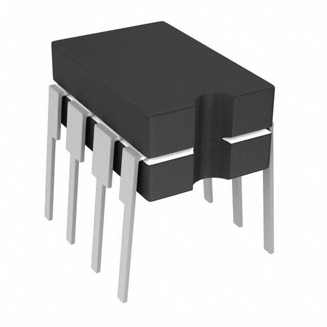
| 产品图片 |
|
| rohs | 符合RoHS无铅 / 符合限制有害物质指令(RoHS)规范要求 |
| 产品系列 | 电源管理 IC,门驱动器,Texas Instruments UCC27211D- |
| 数据手册 | |
| 产品型号 | UCC27211D |
| PCN设计/规格 | |
| 上升时间 | 8 ns |
| 下降时间 | 7 ns |
| 产品 | MOSFET Gate Drivers |
| 产品种类 | 门驱动器 |
| 供应商器件封装 | 8-SOIC |
| 其它名称 | 296-30016-5 |
| 包装 | 管件 |
| 商标 | Texas Instruments |
| 安装类型 | 表面贴装 |
| 安装风格 | SMD/SMT |
| 封装 | Tube |
| 封装/外壳 | 8-SOIC(0.154",3.90mm 宽) |
| 封装/箱体 | SOIC-8 |
| 工作温度 | -40°C ~ 140°C |
| 工厂包装数量 | 75 |
| 延迟时间 | 18ns |
| 最大工作温度 | + 140 C |
| 最小工作温度 | - 40 C |
| 标准包装 | 75 |
| 电压-电源 | 8 V ~ 17 V |
| 电流-峰值 | 4A |
| 电源电压-最大 | 20 V |
| 电源电压-最小 | 7.8 V |
| 电源电流 | 4 A |
| 类型 | High Frequency High-Side/Low-Side |
| 系列 | UCC27211 |
| 输入类型 | 非反相 |
| 输出数 | 2 |
| 输出电流 | 4 A |
| 配置 | Dual, Non-Inverting, TTL Compatible |
| 配置数 | 1 |
| 高压侧电压-最大值(自举) | 120V |


- 商务部:美国ITC正式对集成电路等产品启动337调查
- 曝三星4nm工艺存在良率问题 高通将骁龙8 Gen1或转产台积电
- 太阳诱电将投资9.5亿元在常州建新厂生产MLCC 预计2023年完工
- 英特尔发布欧洲新工厂建设计划 深化IDM 2.0 战略
- 台积电先进制程称霸业界 有大客户加持明年业绩稳了
- 达到5530亿美元!SIA预计今年全球半导体销售额将创下新高
- 英特尔拟将自动驾驶子公司Mobileye上市 估值或超500亿美元
- 三星加码芯片和SET,合并消费电子和移动部门,撤换高东真等 CEO
- 三星电子宣布重大人事变动 还合并消费电子和移动部门
- 海关总署:前11个月进口集成电路产品价值2.52万亿元 增长14.8%


PDF Datasheet 数据手册内容提取
Product Sample & Technical Tools & Support & Folder Buy Documents Software Community UCC27210,UCC27211 SLUSAT7F–NOVEMBER2011–REVISEDDECEMBER2014 UCC2721x 120-V Boot, 4-A Peak, High-Frequency High-Side and Low-Side Driver 1 Features 3 Description • DrivesTwoN-ChannelMOSFETsinHigh-Side The UCC27210 and UCC27211 drivers are based on 1 the popular UCC27200 and UCC27201 MOSFET andLow-SideConfigurationWithIndependent drivers, but offer several significant performance Inputs improvements. Peak output pull-up and pull-down • MaximumBootVoltage120-VDC current has been increased to 4-A source and 4-A • 4-ASink,4-ASourceOutputCurrents sink, and pull-up and pull-down resistance have been reduced to 0.9 Ω, thereby allowing for driving large • 0.9-ΩPullupandPulldownResistance power MOSFETs with minimized switching losses • InputPinsCanTolerate –10Vto20VandAre during the transition through the Miller Plateau of the IndependentofSupplyVoltageRange MOSFET. The input structure is now able to directly • TTLorPseudo-CMOSCompatibleInputVersions handle –10 VDC, which increases robustness and also allows direct interface to gate-drive transformers • 8-Vto17-VVDDOperatingRange,(20-V without using rectification diodes. The inputs are also AbsoluteMaximum) independent of supply voltage and have a maximum • 7.2-nsRiseand5.5-nsFallTimeWith1000-pF ratingof20-V. Load • FastPropagationDelayTimes(18nsTypical) DeviceInformation(1) • 2-nsDelayMatching PARTNUMBER PACKAGE BODYSIZE(NOM) • SymmetricalUndervoltageLockoutforHigh-Side SOIC(8) 4.90mm×3.91mm andLow-SideDriver UCC27210, PowerPAD(8) 4.89mm×3.90mm • AllIndustryStandardPackagesAvailable(SOIC- UCC27211 WSON(10) 4.00mm×4.00mm 8,PowerPAD™SOIC-8,4-mm× 4-mmSON-8 VSON(8) and4-mm×4-mmSON-10) (1) For all available packages, see the orderable addendum at • Specifiedfrom–40to140 °C theendofthedatasheet. 2 Applications • PowerSuppliesforTelecom,Datacom,and Merchant • Half-BridgeandFull-BridgeConverters • Push-PullConverters • High-VoltageSynchronous-BuckConverters • Two-SwitchForwardConverters • Active-ClampForwardConverters • Class-DAudioAmplifiers space TypicalApplication:UCC27210 TypicalApplication:UCC27211 +12V +100V +12V VDD SECSOINDDEARY VDD HB +100V SECCISORINCDDUEAITRY HB CIRCUIT CONPTRWOMLLER HI NTROL DRHIVIE HHOS CONPTRWOMLLER HLII CONTROL DDRRLHOIIVVIEE HHLOOS LI CO DRIVE LO UCC27211 LO VSS UCC27210 +12V VDD +100V VSS HB ISOLATION FEEADNBDACK HLII CONTROL DDRRHIIVVIEE HHLOOS LO UCC27211 1 An IMPORTANT NOTICE at the end of this data sheet addresses availability, warranty, changes, use in safety-critical applications, intellectualpropertymattersandotherimportantdisclaimers.PRODUCTIONDATA.
UCC27210,UCC27211 SLUSAT7F–NOVEMBER2011–REVISEDDECEMBER2014 www.ti.com Table of Contents 1 Features.................................................................. 1 8.1 Overview.................................................................13 2 Applications........................................................... 1 8.2 FunctionalBlockDiagram.......................................14 3 Description............................................................. 1 8.3 FeatureDescription.................................................14 8.4 DeviceFunctionalModes........................................15 4 RevisionHistory..................................................... 2 9 ApplicationandImplementation........................ 16 5 Description(Continued)........................................ 4 9.1 ApplicationInformation............................................16 6 PinConfigurationandFunctions......................... 4 9.2 TypicalApplication .................................................16 7 Specifications......................................................... 5 10 PowerSupplyRecommendations..................... 21 7.1 AbsoluteMaximumRatings......................................5 11 Layout................................................................... 21 7.2 ESDRatings ............................................................6 11.1 LayoutGuidelines.................................................21 7.3 RecommendedOperatingConditions.......................6 11.2 LayoutExample....................................................22 7.4 ThermalInformation..................................................6 11.3 ThermalConsiderations........................................22 7.5 ElectricalCharacteristics...........................................7 12 DeviceandDocumentationSupport................. 23 7.6 SwitchingCharacteristics:PropagationDelays........8 7.7 SwitchingCharacteristics:DelayMatching...............8 12.1 DocumentationSupport........................................23 7.8 SwitchingCharacteristics:OutputRiseandFall 12.2 RelatedLinks........................................................23 Time........................................................................... 8 12.3 Trademarks...........................................................23 7.9 SwitchingCharacteristics:Miscellaneous.................8 12.4 ElectrostaticDischargeCaution............................23 7.10 TypicalCharacteristics..........................................10 12.5 Glossary................................................................23 8 DetailedDescription............................................ 13 13 Mechanical,Packaging,andOrderable Information........................................................... 23 4 Revision History NOTE:Pagenumbersforpreviousrevisionsmaydifferfrompagenumbersinthecurrentversion. ChangesfromRevisionE(August2013)toRevisionF Page • AddedPinConfigurationandFunctionssection,ESDRatingstable,FeatureDescriptionsection,DeviceFunctional Modes,ApplicationandImplementationsection,PowerSupplyRecommendationssection,Layoutsection,Device andDocumentationSupportsection,andMechanical,Packaging,andOrderableInformationsection .............................. 1 ChangesfromRevisionD(November,2012)toRevisionE Page • AddedNote2totheTerminalFunctionsTable...................................................................................................................... 5 • ChangedRepetitivepulsedatafrom-18Vto-(24V-VDD).................................................................................................... 5 • AddedadditionaldetailstoNote2.......................................................................................................................................... 5 • ChangedVoltageonHS,V (repetitivepulse<100ns)datafrom-15to-(24V-VDD)......................................................... 6 HS • Deleted2.4-mAoperatingcurrentminrangeinbothplaces.................................................................................................. 7 • Changedoperatingcurrentmaxrangeextendedto5.2inbothplaces................................................................................. 7 • Deleted1.5minBootvoltageoperatingcurrentrange........................................................................................................... 7 • ChangedBootvoltageoperatingcurrentmaxrangefrom4.2to5.0..................................................................................... 7 • ChangedHBtoV operatingcurrentmaxrangefrom1.1to1.2......................................................................................... 7 SS • ChangedLOGateDriver'sLow-leveloutputvoltagemaxrangefrom0.17to0.19............................................................... 7 • ChangedHOGATEDriver'sLow-leveloutputvoltagemaxrangefrom0.17to0.19............................................................ 7 ChangesfromRevisionC(March,2012)toRevisionD Page • Changedcapacitorrangefrom1.0µFto4.7µF.................................................................................................................... 5 • AddedTerminalFunctionsNotetoHIandLIpindescription................................................................................................. 5 • Changedbullet2intheLayoutRecommendations. ........................................................................................................... 21 • AddedNote:Forsystemsusing........................................................................................................................................... 21 2 SubmitDocumentationFeedback Copyright©2011–2014,TexasInstrumentsIncorporated ProductFolderLinks:UCC27210 UCC27211
UCC27210,UCC27211 www.ti.com SLUSAT7F–NOVEMBER2011–REVISEDDECEMBER2014 • AddedNote:Careshouldbetaken...................................................................................................................................... 21 ChangesfromRevisionB(February)toRevisionC Page • ChangedV operatingcurrentmaxrangeof4.3to4.4inbothplaces................................................................................ 7 DD • ChangedBootvoltageoperatingcurrentmaxrangefrom4.0to4.2..................................................................................... 7 • ChangedHBtoV quiescentcurrentmaxrangefrom0.13to1.0....................................................................................... 7 SS • ChangedHBtoV operatingcurrentmaxrangefrom0.9to1.1......................................................................................... 7 SS • AddedInputUCC27210/11(DDAOnly)values..................................................................................................................... 7 • AddedUnder-VoltageLockout(UVLO)DDAonlyvalues,twoplaces................................................................................... 7 • ChangedLOGateDriver'sLow-leveloutputvoltagemaxrangefrom0.15to0.17............................................................... 7 • ChangedLOGateDriver'sV maxrangefrom0.27to0.29.............................................................................................. 7 LOH • ChangedHOGATEDriver'sLow-leveloutputvoltagemaxrangefrom0.15to0.17............................................................ 7 • ChangedV fallingtoV fallingminvaluefrom17to15..................................................................................................... 8 LI LO • ChangedV fallingtoV fallingminvaluefrom17to15.................................................................................................... 8 HI HO • ChangedV risingtoV risingminvaluefrom18to15....................................................................................................... 8 LI LO • ChangedV risingtoV risingminvaluefrom18to15...................................................................................................... 8 HI HO • ChangedFigure17,OutputCurrentvs.OutputVoltage...................................................................................................... 12 Copyright©2011–2014,TexasInstrumentsIncorporated SubmitDocumentationFeedback 3 ProductFolderLinks:UCC27210 UCC27211
UCC27210,UCC27211 SLUSAT7F–NOVEMBER2011–REVISEDDECEMBER2014 www.ti.com 5 Description (Continued) Theswitchingnode(HSpin)oftheUCC2721xcanhandle–18Vmaximumwhichallowsthehigh-sidechannelto be protected from inherent negative voltages caused parasitic inductance and stray capacitance. The UCC27210 (Pseudo-CMOSinputs)andUCC27211(TTLinputs)haveincreasedhysteresisallowingforinterfacetoanalogor digitalPWMcontrollerswithenhancednoiseimmunity. The low-side and high-side gate drivers are independently controlled and matched to 2 ns between the turnon andturnoffofeachother. An on-chip 120-V rated bootstrap diode eliminates the external discrete diodes. Undervoltage lockout is provided for both the high-side and the low-side drivers providing symmetric turnon and turnoff behavior and forcing the outputslowifthedrivevoltageisbelowthespecifiedthreshold. Both devices are offered in 8-pin SOIC (D), PowerPAD SOIC-8 (DDA), 4-mm × 4-mm SON-8 (DRM) and SON- 10(DPR)packages. 6 Pin Configuration and Functions SOIC-8(D) PowerPadTMSOIC-8(DDA) TOPVIEW TOPVIEW VDD 1 8 LO VDD 1 8 LO Exposed HB 2 7 VSS HB 2 Thermal 7 VSS DiePad HO 3 6 LI HO 3 6 LI HS 4 5 HI HS 4 5 HI SON-8 (DRM) SON-10 (DPR) TOPVIEW TOPVIEW VDD 1 8 LO VDD 1 10 LO Exposed Thermal HB 2 9 VSS HB 2 7 VSS DiePad* HO 3 8 LI HO 3 6 LI HS 4 7 HI HS 4 5 HI NC 5 6 NC 4 SubmitDocumentationFeedback Copyright©2011–2014,TexasInstrumentsIncorporated ProductFolderLinks:UCC27210 UCC27211
UCC27210,UCC27211 www.ti.com SLUSAT7F–NOVEMBER2011–REVISEDDECEMBER2014 PinFunctions PIN I/O DESCRIPTION NAME D/DDA/DRM DPR Positivesupplytothelower-gatedriver.DecouplethispintoV (GND).Typical VDD 1 1 P decouplingcapacitorrangeis0.22µFto4.7µF(See (1)). SS High-sidebootstrapsupply.Thebootstrapdiodeison-chipbuttheexternalbootstrap capacitorisrequired.Connectpositivesideofthebootstrapcapacitortothispin. HB 2 2 P TypicalrangeofHBbypasscapacitoris0.022µFto0.1µF.Thecapacitorvalueis dependantonthegatechargeofthehigh-sideMOSFETandshouldalsobeselected basedonspeedandripplecriteria HO 3 3 O High-sideoutput.Connecttothegateofthehigh-sidepowerMOSFET. High-sidesourceconnection.Connecttosourceofhigh-sidepowerMOSFET. HS 4 4 P Connectthenegativesideofbootstrapcapacitortothispin. HI 5 7 I High-sideinput.(2) LI 6 8 I Low-sideinput.(2) VSS 7 9 G Negativesupplyterminalforthedevicewhichisgenerallygrounded. LO 8 10 O Low-sideoutput.Connecttothegateofthelow-sidepowerMOSFET. N/C — 5/6 — Notconnected. UsedontheDDA,DRMandDPRpackagesonly.ElectricallyreferencedtoV PowerPAD SS ™(3) Pad Pad G (GND).ConnecttoalargethermalmasstraceorGNDplanetodramaticallyimprove thermalperformance. (1) Forcoldtemperatureapplicationswerecommendtheuppercapacitancerange.AttentionshouldalsobemadetoPCBlayout-see Layout. (2) HIorLIinputisassumedtoconnecttoalowimpedancesourcesignal.Thesourceoutputimpedanceisassumedlessthan100Ω.Ifthe sourceimpedanceisgreaterthan100Ω,addabypassingcapacitor,each,betweenHIandVSSandbetweenLIandVSS.Theadded capacitorvaluedependsonthenoiselevelspresentedonthepins,typicallyfrom1nFto10nFshouldbeeffectivetoeliminatethe possiblenoiseeffect.Whennoiseispresentontwopins,HIorLI,theeffectistocauseHOandLOmalfunctionstohavewronglogic outputs. (3) ThePowerPAD™isnotdirectlyconnectedtoanyleadsofthepackage.Howeveritiselectricallyandthermallyconnectedtothe substratewhichisthegroundofthedevice. 7 Specifications 7.1 Absolute Maximum Ratings(1) overoperatingfree-airtemperaturerange(unlessotherwisenoted) MIN MAX UNIT Supplyvoltagerange,V (2),V -V –0.3 20 DD HB HS InputvoltagesonLIandHI,V ,V –10 20 LI HI DC –0.3 V +0.3 DD OutputvoltageonLO,V LO Repetitivepulse<100ns(3) –2 V +0.3 DD DC V –0.3 V +0.3 V HS HB OutputvoltageonHO,V HO Repetitivepulse<100ns(3) V –2 V +0.3 HS HB DC –1 115 VoltageonHS,V HS Repetitivepulse<100ns(3) –(24V-VDD) 115 VoltageonHB,V –0.3 120 HB Operatingvirtualjunctiontemperature,T –40 150 J °C Leadtemperature(soldering,10sec.) 300 Storagetemperature,T –65 150 °C stg (1) StressesbeyondthoselistedunderAbsoluteMaximumRatingsmaycausepermanentdamagetothedevice.Thesearestressratings only,andfunctionaloperationofthedeviceattheseoranyotherconditionsbeyondthoseindicatedunderRecommendedOperating Conditionsisnotimplied.Exposuretoabsolute-maximum-ratedconditionsforextendedperiodsmayaffectdevicereliability. (2) AllvoltagesarewithrespecttoVSSunlessotherwisenoted.Currentsarepositiveinto,negativeoutofthespecifiedterminal. (3) Verifiedatbenchcharacterization.VDDisthevalueusedinanapplicationdesign. Copyright©2011–2014,TexasInstrumentsIncorporated SubmitDocumentationFeedback 5 ProductFolderLinks:UCC27210 UCC27211
UCC27210,UCC27211 SLUSAT7F–NOVEMBER2011–REVISEDDECEMBER2014 www.ti.com 7.2 ESD Ratings VALUE UNIT Humanbodymodel(HBM),perANSI/ESDA/JEDECJS-001(1) ±2000 V(ESD) Electrostaticdischarge Charged-devicemodel(CDM),perJEDECspecificationJESD22- ±1000 V C101(2) (1) JEDECdocumentJEP155statesthat500-VHBMallowssafemanufacturingwithastandardESDcontrolprocess. (2) JEDECdocumentJEP157statesthat250-VCDMallowssafemanufacturingwithastandardESDcontrolprocess. 7.3 Recommended Operating Conditions allvoltagesarewithrespecttoV ;currentsarepositiveintoandnegativeoutofthespecifiedterminal.–40°C<T =T < SS J A 140°C(unlessotherwisenoted) MIN TYP MAX UNIT Supplyvoltagerange,V ,V -V 8 12 17 DD HB HS VoltageonHS,V –1 105 HS VoltageonHS,V (repetitivepulse<100ns) –(24V-VDD) 110 V HS V +8, V +17, VoltageonHB,V HS HS HB V –1 115 DD VoltageslewrateonHS 50 V/ns Operatingjunctiontemperaturerange –40 140 °C 7.4 Thermal Information UCC27210,UCC27211 THERMALMETRIC D DDA DRM DPR UNIT 8PINS 8PINS 8PINS 10PINS θ Junction-to-ambientthermalresistance(1) 111.8 37.7 33.9 36.8 JA θ Junction-to-case(top)thermalresistance(2) 56.9 47.2 33.2 36.0 JCtop θ Junction-to-boardthermalresistance(3) 53.0 9.6 11.4 14.0 JB °C/W ψ Junction-to-topcharacterizationparameter(4) 7.8 2.8 0.4 0.3 JT ψ Junction-to-boardcharacterizationparameter(5) 52.3 9.4 11.7 14.2 JB θ Junction-to-case(bottom)thermalresistance(6) n/a 3.6 2.3 3.4 JCbot (1) Thejunction-to-ambientthermalresistanceundernaturalconvectionisobtainedinasimulationonaJEDEC-standard,high-Kboard,as specifiedinJESD51-7,inanenvironmentdescribedinJESD51-2a. (2) Thejunction-to-case(top)thermalresistanceisobtainedbysimulatingacoldplatetestonthepackagetop.NospecificJEDEC- standardtestexists,butaclosedescriptioncanbefoundintheANSISEMIstandardG30-88. (3) Thejunction-to-boardthermalresistanceisobtainedbysimulatinginanenvironmentwitharingcoldplatefixturetocontrolthePCB temperature,asdescribedinJESD51-8. (4) Thejunction-to-topcharacterizationparameter,ψ ,estimatesthejunctiontemperatureofadeviceinarealsystemandisextracted JT fromthesimulationdataforobtainingR ,usingaproceduredescribedinJESD51-2a(sections6and7). θJA (5) Thejunction-to-boardcharacterizationparameter,ψ ,estimatesthejunctiontemperatureofadeviceinarealsystemandisextracted JB fromthesimulationdataforobtainingR ,usingaproceduredescribedinJESD51-2a(sections6and7). θJA (6) Thejunction-to-case(bottom)thermalresistanceisobtainedbysimulatingacoldplatetestontheexposed(power)pad.Nospecific JEDECstandardtestexists,butaclosedescriptioncanbefoundintheANSISEMIstandardG30-88. Spacer 6 SubmitDocumentationFeedback Copyright©2011–2014,TexasInstrumentsIncorporated ProductFolderLinks:UCC27210 UCC27211
UCC27210,UCC27211 www.ti.com SLUSAT7F–NOVEMBER2011–REVISEDDECEMBER2014 7.5 Electrical Characteristics V =V =12V,V =V =0V,noloadonLOorHO,T =T =–40°Cto140°C,(unlessotherwisenoted) DD HB HS SS A J PARAMETER TESTCONDITIONS MIN TYP MAX UNIT SUPPLYCURRENTS I V quiescentcurrent V(LI)=V(HI)=0V 0.05 0.085 0.17 DD DD I UCC27210 2.6 5.2 DDO V operatingcurrent f=500kHz,C =0 DD LOAD UCC27211 2.5 5.2 mA I Bootvoltagequiescentcurrent V(LI)=V(HI)=0V 0.015 0.065 0.1 HB I Bootvoltageoperatingcurrent f=500kHz,C =0 2.5 5.0 HBO LOAD I HBtoV quiescentcurrent V(HS)=V(HB)=115V 0.0005 1.0 µA HBS SS I HBtoV operatingcurrent f=500kHz,C =0 0.07 1.2 mA HBSO SS LOAD INPUT V Inputvoltagethreshold UCC27210 4.2 5.0 5.8 HIT UCC27210(DDAonly) 4.2 5.0 5.9 V Inputvoltagethreshold UCC27210 2.4 3.2 4.0 V LIT UCC27210(DDAonly) 2.4 3.2 4.0 V Inputvoltagehysteresis 1.8 IHYS UCC27210 R Inputpulldownresistance 102 kΩ IN V Inputvoltagethreshold UCC27211 1.9 2.3 2.7 HIT UCC27211(DDAonly) 1.9 2.3 2.8 V V Inputvoltagethreshold UCC27211 1.3 1.6 1.9 LIT UCC27211(DDAonly) 1.3 1.6 2.1 V Inputvoltagehysteresis 700 mV IHYS UCC27211 R Inputpulldownresistance 68 kΩ IN UNDERVOLTAGELOCKOUT(UVLO) V V turnonthreshold 6.2 7.0 7.8 DDR DD DDAonly 5.8 7.0 8.1 V Hysteresis 0.5 DDHYS V V V turnonthreshold 5.6 6.7 7.9 HBR HB DDAonly 5.3 6.7 8.0 V Hysteresis 1.1 HBHYS BOOTSTRAPDIODE V Low-currentforwardvoltage I =100µA 0.65 0.8 F VDD-HB V V High-currentforwardvoltage I =100mA 0.85 0.95 FI VDD-HB R Dynamicresistance,ΔVF/ΔI I =100mAand80mA 0.3 0.5 0.85 Ω D VDD-HB LOGATEDRIVER V Low-leveloutputvoltage I =100mA 0.05 0.09 0.19 LOL LO V V Highleveloutputvoltage I =-100mA,V =V -V 0.1 0.16 0.29 LOH LO LOH DD LO Peakpull-upcurrent(1) V =0V 3.7 LO A Peakpull-downcurrent(1) V =12V 4.5 LO HOGATEDRIVER V Low-leveloutputvoltage I =100mA 0.05 0.09 0.19 HOL HO V V High-leveloutputvoltage I =-100mA,V =V -V 0.1 0.16 0.29 HOH HO HOH HB HO Peakpull-upcurrent(1) V =0V 3.7 HO A Peakpull-downcurrent(1) V =12V 4.5 HO (1) Ensuredbydesign. Copyright©2011–2014,TexasInstrumentsIncorporated SubmitDocumentationFeedback 7 ProductFolderLinks:UCC27210 UCC27211
UCC27210,UCC27211 SLUSAT7F–NOVEMBER2011–REVISEDDECEMBER2014 www.ti.com 7.6 Switching Characteristics: Propagation Delays overoperatingfree-airtemperaturerange(unlessotherwisenoted) PARAMETER TESTCONDITIONS MIN TYP MAX UNIT T V fallingtoV falling UCC27210,C =0 15 21 37 DLFF LI LO LOAD T V fallingtoV falling 15 21 37 DHFF HI HO T V risingtoV rising 15 24 46 DLRR LI LO T V risingtoV rising 15 24 46 DHRR HI HO ns T V fallingtoV falling UCC27211,C =0 10 17 30 DLFF LI LO LOAD T V fallingtoV falling 10 17 30 DHFF HI HO T V risingtoV rising 10 18 40 DLRR LI LO T V risingtoV rising 10 18 40 DHRR HI HO 7.7 Switching Characteristics: Delay Matching overoperatingfree-airtemperaturerange(unlessotherwisenoted) PARAMETER TESTCONDITIONS MIN TYP MAX UNIT T FromHOOFFtoLOON T =25°C 3 11 MON J ns T =–40°Cto140°C 3 14 J UCC27210 T FromLOOFFtoHOON T =25°C 3 11 MOFF J ns T =–40°Cto140°C 3 14 J T FromHOOFFtoLOON T =25°C 2 9.5 MON J ns T =–40°Cto140°C 2 14 J UCC27211 T FromLOOFFtoHOON T =25°C 2 9.5 MOFF J ns T =–40°Cto140°C 2 14 J 7.8 Switching Characteristics: Output Rise and Fall Time overoperatingfree-airtemperaturerange(unlessotherwisenoted) PARAMETER TESTCONDITIONS MIN TYP MAX UNIT t LOrisetime C =1000pF,from10%to90% 7.2 R LOAD t HOrisetime 7.2 R ns t LOfalltime C =1000pF,from90%to10% 5.5 F LOAD t HOfalltime 5.5 F t LO,HO C =0.1µF,(3Vto9V) 0.36 0.6 R LOAD µs t LO,HO C =0.1µF,(9Vto3V) 0.15 0.4 F LOAD 7.9 Switching Characteristics: Miscellaneous overoperatingfree-airtemperaturerange(unlessotherwisenoted) PARAMETER TESTCONDITIONS MIN TYP MAX UNIT Minimuminputpulsewidththatchangestheoutput 50 ns Bootstrapdiodeturnofftime(1)(2) I =20mA,I =0.5A(3) 20 F REV (1) Ensuredbydesign. (2) I :Forwardcurrentappliedtobootstrapdiode,I :Reversecurrentappliedtobootstrapdiode. F REV (3) TypicalvaluesforT =25°C. A 8 SubmitDocumentationFeedback Copyright©2011–2014,TexasInstrumentsIncorporated ProductFolderLinks:UCC27210 UCC27211
UCC27210,UCC27211 www.ti.com SLUSAT7F–NOVEMBER2011–REVISEDDECEMBER2014 LI Input (HI, LI) HI TDLRR, TDHRR LO Output (HO, LO) TDLFF, TDHFF HO TMON TMOFF Figure1. TimingDiagrams Copyright©2011–2014,TexasInstrumentsIncorporated SubmitDocumentationFeedback 9 ProductFolderLinks:UCC27210 UCC27211
UCC27210,UCC27211 SLUSAT7F–NOVEMBER2011–REVISEDDECEMBER2014 www.ti.com 7.10 Typical Characteristics 100 100 T = 25°C UCC27210, VDD = 12V µA) A) cent Current ( 6800 ng Current (m 110 − QuiesB 40 − Operati 0.1 CCCLLL===000pppFFF,,, TTT===−21544°00C°°CC , IDDH 20 UCC27210/1 IDD I DDO CCLL==11000000ppFF,, TT==2154°0C°C I UCC27210/1 IHB CL=4700pF, T=140°C 0 0.01 0 2 4 6 8 10 12 14 16 18 20 10 100 1000 VDD = VHB − Supply Voltage (V) G001 Frequency (kHz) G002 Figure2.QuiescentCurrentvsSupplyVoltage Figure3.UCC27210IDDOperatingCurrentvsFrequency 100 100 UCC27211, VDD = 12V UCC27210/1, VHB − VHS = 12V A) A) m m nt ( 10 nt ( 10 e e urr urr C C ng 1 ng 1 erati CL=0pF, T=−40°C erati CL=0pF, T=−40°C Op CL=0pF, T=25°C Op CL=0pF, T=25°C − 0.1 CL=0pF, T=140°C − 0.1 CL=0pF, T=140°C DO CL=1000pF, T=25°C BO CL=1000pF, T=25°C ID CL=1000pF, T=140°C IH CL=1000pF, T=140°C CL=4700pF, T=140°C CL=4700pF, T=140°C 0.01 0.01 10 100 1000 10 100 1000 Frequency (kHz) Frequency (kHz) G003 G004 Figure4.UCC27211IDDOperatingCurrentvsFrequency Figure5.BootVoltageOperatingCurrentvsFrequency(HB toHS) 6 6 V) T = 25°C V) VDD = 12V e ( 5 e ( 5 g g a a olt 4 olt 4 V V d d ol 3 ol 3 h h s s e e hr 2 hr 2 T T ut ut np 1 UCC27210, Rising np 1 UCC27210, Rising HI, LI − I 0 UUUCCCCCC222777222111011,,, FRFaaislllliiinnnggg HI, LI − I 0 UUUCCCCCC222777222111011,,, FRFaaislllliiinnnggg −1 −1 8 12 16 20 −40 −20 0 20 40 60 80 100 120 140 VDD − Supply Voltage (V) G005 Temperature (°C) G006 Figure6.UCC27210andUCC27211InputThresholdvs Figure7.UCC27210andUCC27211InputThresholdsvs SupplyVoltage Temperature 10 SubmitDocumentationFeedback Copyright©2011–2014,TexasInstrumentsIncorporated ProductFolderLinks:UCC27210 UCC27211
UCC27210,UCC27211 www.ti.com SLUSAT7F–NOVEMBER2011–REVISEDDECEMBER2014 Typical Characteristics (continued) 0.32 0.2 IHO=ILO= 100mA IHO=ILO= 100mA V) 0.28 V) e ( e ( 0.16 ag 0.24 ag olt olt ut V 0.2 ut V 0.12 p p ut 0.16 ut O O O O 0.08 H 0.12 H O/ O/ V − LOH00..0048 UUUCCCCCC222777222111000///111,,, VVVDDDDDD===VVVHHHBBB===811V26VV V − LOL0.04 UUUCCCCCC222777222111000///111,,, VVVDDDDDD===VVVHHHBBB===811V26VV UCC27210/1, VDD=VHB=20V UCC27210/1, VDD=VHB=20V 0 0 −40 −20 0 20 40 60 80 100 120 140 −40 −20 0 20 40 60 80 100 120 140 Temperature (°C) Temperature (°C) G007 G008 Figure8.LOandHOHighLevelOutputVoltagevs Figure9.LOandHOLowLevelOutputVoltagevs Temperature Temperature 8 1.5 7.6 1.2 7.2 V) V) hreshold ( 66..48 ysteresis ( 00..69 T H 6 0.3 5.6 VDD Rising Threshold VDD UVLO Hysteresis HB Rising Threshold HB UVLO Hysteresis 5.2 0 −40 −20 0 20 40 60 80 100 120 140 −40 −20 0 20 40 60 80 100 120 140 Temperature (°C) Temperature (°C) G009 G010 Figure10.UndervoltageLockoutThresholdvsTemperature Figure11.UndervoltageLockoutThresholdHysteresisvs Temperature 40 32 36 UCC27210, VDD=VHB=12V UCC27211, VDD=VHB=12V 32 s) s) 24 y (n 28 y (n ela 24 ela D D n 20 n 16 o o ati 16 ati g g a a Prop 12 TDLRR Prop 8 TDLRR 8 TDLFF TDLFF TDHRR TDHRR 4 TDHFF TDHFF 0 0 −40 −20 0 20 40 60 80 100 120 140 −40 −20 0 20 40 60 80 100 120 140 Temperature (°C) Temperature (°C) G011 G012 Figure12.UCC27210PropagationDelaysvsTemperature Figure13.UCC27211PropagationDelaysvsTemperature Copyright©2011–2014,TexasInstrumentsIncorporated SubmitDocumentationFeedback 11 ProductFolderLinks:UCC27210 UCC27211
UCC27210,UCC27211 SLUSAT7F–NOVEMBER2011–REVISEDDECEMBER2014 www.ti.com Typical Characteristics (continued) 32 32 UCC27210, T=25°C UCC27211, T=25°C 28 28 s) 24 s) 24 n n ay ( 20 ay ( 20 el el D D n 16 n 16 o o ati ati g 12 g 12 a a p p Pro 8 TDLRR Pro 8 TDLRR TDLFF TDLFF 4 TDHRR 4 TDHRR TDHFF TDHFF 0 0 8 12 16 20 8 12 16 20 VDD=VHB − Supply Voltage (V) G012 VDD=VHB − Supply Voltage (V) G014 Figure14.UCC27210PropagationDelaysvsSupplyVoltage Figure15.UCC27211PropagationDelaysvsSupplyVoltage 10 5 VDD=VHB=12V VDD=VHB=12V 8 A) 4 ng (ns) 6 Current ( 3 elay Matchi 24 − Output O 2 D UUCCCC2277221100,, TTMMoonff , IOH 1 0 UCC27211, TMon IL Pull Down Current UCC27211, TMoff Pull Up Current −2 0 −40 −20 0 20 40 60 80 100 120 140 0 2 4 6 8 10 12 Temperature (°C) G015 VLO, VHO − Output Voltage (V) G016 Figure16.DelayMatchingvsTemperature Figure17.OutputCurrentvsOutputVoltage 100 10 A) m nt ( 1 e urr C e 0.1 d o Di 0.01 0.001 500 550 600 650 700 750 800 850 Diode Voltage (mV) G017 Figure18.DiodeCurrentvsDiodeVoltage 12 SubmitDocumentationFeedback Copyright©2011–2014,TexasInstrumentsIncorporated ProductFolderLinks:UCC27210 UCC27211
UCC27210,UCC27211 www.ti.com SLUSAT7F–NOVEMBER2011–REVISEDDECEMBER2014 8 Detailed Description 8.1 Overview The UCC27210 and UCC27211 devices represent Texas Instruments’ latest generation of high voltage gate drivers which are designed to drive both the high side and low side of N-channel MOSFETs in a half-/full-bridge or synchronous buck configuration. The floating high-side driver can operate with supply voltages of up to 120 V. This allows for N-channel MOSFET control in half-bridge, full-bridge, push pull, two-switch forward and active clampforwardconverters. The UCC27210 and UCC27211 devices feature 4-A source/sink capability, industry best-in-class switching characteristics and a host of other features listed in Table 1. These features combine to ensure efficient, robust andreliableoperationinhigh-frequencyswitchingpowercircuits. Table1.UCC27210andUCC27211Highlights FEATURE BENEFIT HighpeakcurrentidealfordrivinglargepowerMOSFETswith 4-Asourceandsinkcurrentwith0.9-Ωoutputresistance minimalpowerloss(fast-drivecapabilityatMillerplateau) Increasedrobustnessandabilitytohandleunder/overshoot.Can Inputpins(HIandLI)candirectlyhandle–10VDCupto20VDC interfacedirectlytogate-drivetransformerswithouthavingtouse rectificationdiodes 120-Vinternalbootdiode Providesvoltagemargintomeettelecom100-Vsurgerequirements Allowsthehigh-sidechanneltohaveextraprotectionfrominherent Switchnode(HSpin)abletohandle–18Vmaximumfor100ns negativevoltagescausedparasiticinductanceandstray capacitance. RobustESDcircuitrytohandlevoltagespikes ExcellentimmunitytolargedV/dTconditions Best-in-classswitchingcharacteristicsandextremelylow-pulse 18-nspropagationdelaywith7.2-ns/5.5-nsrise/fallTimes transmissiondistortion 2-ns(typ)delaymatchingbetweenchannels Avoidstransformervolt-secondoffsetinbridge SymmetricalUVLOcircuit Ensureshigh-sideandlow-sideshutdownatthesametime CMOSoptimizedthresholdorTTLoptimizedthresholdswith ComplementarytoanalogordigitalPWMcontrollers.Increased increasedhysteresis hysteresisoffersaddednoiseimmunity In the UCC27210 and UCC27211 devices, the high side and low side each have independent inputs which allow maximum flexibility of input control signals in the application. The boot diode for the high-side driver bias supply is internal to the UCC27210 and UCC27211. The UCC27210 is the Pseudo-CMOS compatible input version and the UCC27211 is the TTL or logic compatible version. The high-side driver is referenced to the switch node (HS) which is typically the source pin of the high-side MOSFET and drain pin of the low-side MOSFET. The low-side driver is referenced to V which is typically ground. The functions contained are the input stages, UVLO SS protection,levelshift,bootdiode,andoutputdriverstages. Copyright©2011–2014,TexasInstrumentsIncorporated SubmitDocumentationFeedback 13 ProductFolderLinks:UCC27210 UCC27211
UCC27210,UCC27211 SLUSAT7F–NOVEMBER2011–REVISEDDECEMBER2014 www.ti.com 8.2 Functional Block Diagram 2 HB UVLO Level 3 HO Shift 4 HS HI 5 VDD 1 UVLO 8 LO LI 6 7 VSS Copyright © 2016,Texas Instruments Incorporated 8.3 Feature Description 8.3.1 InputStages The input stages provide the interface to the PWM output signals. The input impedance of the UCC27210 is 100 kΩ nominal and input capacitance is approximately 2 pF. The 100 kΩ is a pull-down resistance to V (ground). SS The UCC27210 Pseudo-CMOS input structure has been designed to provide large hysteresis and at the same time to allows interfacing to a multitude of analog or digital PWM controllers. In some CMOS designs, the input thresholds are determined as a percentage of VDD. By doing so, the high-level input threshold can become unreasonably high and unusable. The UCC27210 recognizes the fact that VDD levels are trending downward and it therefore provides a rising threshold with 5.0 V (typical) and falling threshold with 3.2 V (typical). The input hysteresisoftheUCC27210is1.8V(typical). The input stages of the UCC27211 have impedance of 70 kΩ nominal and input capacitance is approximately 2 pF. Pull-down resistance to V (ground) is 70 kΩ. The logic level compatible input provides a rising threshold of SS 2.3Vandafallingthresholdof1.6V. 8.3.2 UndervoltageLockout(UVLO) The bias supplies for the high-side and low-side drivers have UVLO protection. V as well as V to V DD HB HS differential voltages are monitored. The V UVLO disables both drivers when V is below the specified DD DD threshold. The rising V threshold is 7.0 V with 0.5-V hysteresis. The VHB UVLO disables only the high-side DD driver when the V to V differential voltage is below the specified threshold. The V UVLO rising threshold is HB HS HB 6.7Vwith1.1-Vhysteresis. 8.3.3 LevelShift The level shift circuit is the interface from the high-side input to the high-side driver stage which is referenced to the switch node (HS). The level shift allows control of the HO output referenced to the HS pin and provides excellentdelaymatchingwiththelow-sidedriver. 14 SubmitDocumentationFeedback Copyright©2011–2014,TexasInstrumentsIncorporated ProductFolderLinks:UCC27210 UCC27211
UCC27210,UCC27211 www.ti.com SLUSAT7F–NOVEMBER2011–REVISEDDECEMBER2014 Feature Description (continued) 8.3.4 BootDiode The boot diode necessary to generate the high-side bias is included in the UCC27210 and UCC27211 family of drivers. The diode anode is connected to V and cathode connected to V . With the V capacitor connected DD HB HB to HB and the HS pins, the V capacitor charge is refreshed every switching cycle when HS transitions to HB ground. The boot diode provides fast recovery times, low diode resistance, and voltage rating margin to allow for efficientandreliableoperation. 8.3.5 OutputStages TheoutputstagesaretheinterfacetothepowerMOSFETsinthepowertrain.Highslewrate,lowresistanceand high peak current capability of both output drivers allow for efficient switching of the power MOSFETs. The low- sideoutputstageisreferencedfromV toV andthehighsideisreferencedfromV toV . DD SS HB HS 8.4 Device Functional Modes The device operates in normal mode and UVLO mode. See the Undervoltage Lockout (UVLO) section for information on UVLO operation mode. In the normal mode the output state is dependent on states of the HI and LIpins.Table2liststheoutputstatesfordifferentinputpincombinations. Table2.DeviceLogicTable HIPin LIPin HO(1) LO(2) L L L L L H L H H L H L H H H H (1) HOismeasuredwithrespecttoHS. (2) LOismeasuredwithrespecttoVSS. Copyright©2011–2014,TexasInstrumentsIncorporated SubmitDocumentationFeedback 15 ProductFolderLinks:UCC27210 UCC27211
UCC27210,UCC27211 SLUSAT7F–NOVEMBER2011–REVISEDDECEMBER2014 www.ti.com 9 Application and Implementation NOTE Information in the following applications sections is not part of the TI component specification, and TI does not warrant its accuracy or completeness. TI’s customers are responsible for determining suitability of components for their purposes. Customers should validateandtesttheirdesignimplementationtoconfirmsystemfunctionality. 9.1 Application Information Toeffectfastswitchingofpowerdevicesandreduceassociatedswitchingpowerlosses,apowerfulgatedriveris employed between the PWM output of controllers and the gates of the power semiconductor devices. Also, gate drivers are indispensable when it is impossible for the PWM controller to directly drive the gates of the switching devices. With the advent of digital power, this situation will be often encountered because the PWM signal from the digital controller is often a 3.3-V logic signal which cannot effectively turn on a power switch. Level shifting circuitry is needed to boost the 3.3-V signal to the gate-drive voltage (such as 12 V) in order to fully turn on the power device and minimize conduction losses. Traditional buffer drive circuits based on NPN/PNP bipolar transistors in totem-pole arrangement, being emitter follower configurations, prove inadequate with digital power becausetheylacklevel-shiftingcapability.Gatedriverseffectivelycombineboththelevel-shiftingandbuffer-drive functions. Gate drivers also find other needs such as minimizing the effect of high-frequency switching noise by locating the high-current driver physically close to the power switch, driving gate-drive transformers and controlling floating power-device gates, reducing power dissipation and thermal stress in controllers by moving gatechargepowerlossesfromthecontrollerintothedriver. Finally, emerging wide band-gap power device technologies such as GaN based switches, which are capable of supporting very high switching frequency operation, are driving very special requirements in terms of gate drive capability. These requirements include operation at low VDD voltages (5 V or lower), low propagation delays and availability in compact, low-inductance packages with good thermal capability. In summary gate-driver devices are extremely important components in switching power, combining benefits of high-performance, low-cost componentcountandboard-spacereductionaswellassimplifiedsystemdesign. 9.2 Typical Application +12V +100V SECONDARY V DD SIDE HB CIRCUIT HI DRIVE HO OL HI PWM R HS CONTROLLER T N LI O C DRIVE LO LO UCC27210 VSS ISOLATION AND FEEDBACK Figure19. TypicalApplicationDiagram:UCC27210 16 SubmitDocumentationFeedback Copyright©2011–2014,TexasInstrumentsIncorporated ProductFolderLinks:UCC27210 UCC27211
UCC27210,UCC27211 www.ti.com SLUSAT7F–NOVEMBER2011–REVISEDDECEMBER2014 Typical Application (continued) +12V V +100V SECONDARY DD SIDE HB CIRCUIT HI DRIVE HO L HI O PWM R HS CONTROLLER T N LI O C DRIVE LO LO UCC27211 VSS +12V VDD +100V HB HI DRIVE HO L HI O R HS T N LI O C DRIVE LO LO UCC27211 Figure20. TypicalApplicationDiagram:UCC27211 9.2.1 DesignRequirements Table3.DesignSpecifications DESIGNPARAMETER EXAMPLEVALUE Supplyvoltage,VDD 12V VoltageonHS,VHS 0Vto100V VoltageonHB,VHB 12Vto112V Outputcurrentrating,IO –4Ato4A Operatingfrequency 500kHz Copyright©2011–2014,TexasInstrumentsIncorporated SubmitDocumentationFeedback 17 ProductFolderLinks:UCC27210 UCC27211
UCC27210,UCC27211 SLUSAT7F–NOVEMBER2011–REVISEDDECEMBER2014 www.ti.com 9.2.2 DetailedDesignProcedure 9.2.2.1 InputThresholdType The UCC27210 and UCC27211 have an input maximum voltage range from –10 V to 20 V. This increased robustness means that both parts can be directly interfaced to gate drive transformers. The UCC27210 features pseudo CMOS compatible inputs and UCC27211 features TTL compatible input threshold logic, with wide hysteresis. The threshold voltage levels are low voltage and independent of the VDD supply voltage, which allows compatibility with both logic-level input signals from microcontrollers as well as higher-voltage input signals from analog controllers. See the Electrical Characteristics table for the actual input threshold voltage levelsandhysteresisspecificationsfortheUCC27210andUCC27211devices. 9.2.2.2 V BiasSupplyVoltage DD The bias supply voltage to be applied to the VDD pin of the device should never exceed the values listed in the Recommended Operating Conditions table. However, different power switches demand different voltage levels to be applied at the gate terminals for effective turnon and turnoff. With certain power switches, a positive gate voltage may be required for turnon and a negative gate voltage may be required for turnoff, in which case the VDD bias supply equals the voltage differential. With a wide operating range from 8 V to 17 V, the UCC27210 and UCC27211 devices can be used to drive a variety of power switches, such as Si MOSFETs, IGBTs, and wide-bandgap power semiconductors (such as GaN, certain types of which allow no higher than 6 V to be appliedtothegateterminals). 9.2.2.3 PeakSourceandSinkCurrents Generally, the switching speed of the power switch during turnon and turnoff should be as fast as possible in order to minimize switching power losses. The gate driver device must be able to provide the required peak current for achieving the targeted switching speeds with the targeted power MOSFET. The system requirement for the switching speed is typically described in terms of the slew rate of the drain-to-source voltage of the power MOSFET (such as dV /dt). For example, the system requirement might state that a SPP20N60C3 power DS MOSFET must be turned-on with a dV /dt of 20V/ns or higher with a DC bus voltage of 400 V in a continuous- DS conduction-mode (CCM) boost PFC-converter application. This type of application is an inductive hard-switching application and reducing switching power losses is critical. This requirement means that the entire drain-to- source voltage swing during power MOSFET turnon event (from 400 V in the OFF state to V in on state) DS(on) must be completed in approximately 20 ns or less. When the drain-to-source voltage swing occurs, the Miller charge of the power MOSFET (QGD parameter in SPP20N60C3 data sheet is 33 nC typical) is supplied by the peak current of gate driver. According to power MOSFET inductive switching mechanism, the gate-to-source voltage of the power MOSFET at this time is the Miller plateau voltage, which is typically a few volts higher than thethresholdvoltageofthepowerMOSFET,V . GS(TH) To achieve the targeted dV /dt, the gate driver must be capable of providing the Q charge in 20 ns or less. In DS GD other words a peak current of 1.65 A (= 33 nC / 20 ns) or higher must be provided by the gate driver. The UCC27210 and UCC27211 gate driver is capable of providing 4-A peak sourcing current which clearly exceeds the design requirement and has the capability to meet the switching speed needed. The 2.4x overdrive capability provides an extra margin against part-to-part variations in the Q parameter of the power MOSFET along with GD additional flexibility to insert external gate resistors and fine tune the switching speed for efficiency versus EMI optimizations. However, in practical designs the parasitic trace inductance in the gate drive circuit of the PCB will have a definitive role to play on the power MOSFET switching speed. The effect of this trace inductance is to limit the dI/dt of the output current pulse of the gate driver. In order to illustrate this, consider output current pulse waveform from the gate driver to be approximated to a triangular profile, where the area under the triangle (½ ×I × time) would equal the total gate charge of the power MOSFET (QG parameter in SPP20N60C3 power PEAK MOSFETdatasheet=87nCtypical).IftheparasitictraceinductancelimitsthedI/dtthenasituationmayoccurin which the full peak current capability of the gate driver is not fully achieved in the time required to deliver the QG required for the power MOSFET switching. In other words the time parameter in the equation would dominate and the I value of the current pulse would be much less than the true peak current capability of the device, PEAK while the required QG is still delivered. Because of this, the desired switching speed may not be realized, even when theoretical calculations indicate the gate driver is capable of achieving the targeted switching speed. Thus, placing the gate driver device very close to the power MOSFET and designing a tight gate drive-loop with minimalPCBtraceinductanceisimportanttorealizethefullpeak-currentcapabilityofthegatedriver. 18 SubmitDocumentationFeedback Copyright©2011–2014,TexasInstrumentsIncorporated ProductFolderLinks:UCC27210 UCC27211
UCC27210,UCC27211 www.ti.com SLUSAT7F–NOVEMBER2011–REVISEDDECEMBER2014 9.2.2.4 PropagationDelay The acceptable propagation delay from the gate driver is dependent on the switching frequency at which it is used and the acceptable level of pulse distortion to the system. The UCC27210 features 21 ns and the UCC27211 features 17 ns (typical) propagation delays which ensures very little pulse distortion and allows operation at very high-frequencies. See the Electrical Characteristics table for the propagation and switching characteristicsoftheUCC27210andUCC27211devices. 9.2.2.5 PowerDissipation PowerdissipationofthegatedriverhastwoportionsasshowninEquation1. P =P +P (1) DISS DC SW The DC portion of the power dissipation is PDC = I x VDD where I is the quiescent current for the driver. The Q Q quiescentcurrentisthecurrentconsumedbythedevicetobiasallinternalcircuitssuchasinputstage,reference voltage, logic circuits, protections, and also any current associated with switching of internal devices when the driver output changes state (such as charging and discharging of parasitic capacitances, parasitic shoot-through, and so forth). The UCC27210 and UCC27211 features very low quiescent currents (less than 0.17 mA, refer to the Electrical Characteristics table and contain internal logic to eliminate any shoot-through in the output driver stage. Thus the effect of the PDC on the total power dissipation within the gate driver can be safely assumed to be negligible. The power dissipated in the gate-driver package during switching (PSW) depends on the following factors: • Gate charge required of the power device (usually a function of the drive voltage VG, which is very close to inputbiassupplyvoltageVDD) • Switchingfrequency • Use of external gate resistors. When a driver device is tested with a discrete, capacitive load calculating the power that is required from the bias supply is fairly simple. The energy that must be transferred from the bias supplytochargethecapacitorisgivenbyEquation2. EG=½C V ²f LOAD DD SW where • C isloadcapacitor LOAD • V isbiasvoltagefeedingthedriver (2) DD There is an equal amount of energy dissipated when the capacitor is charged. This leads to a total power loss givenbyEquation3. PG=C V ²f LOAD DD SW where • f istheswitchingfrequency (3) SW TheswitchingloadpresentedbyapowerMOSFET/IGBTisconvertedtoanequivalentcapacitancebyexamining the gate charge required to switch the device. This gate charge includes the effects of the input capacitance plus theaddedchargeneededtoswingthedrainvoltageofthepowerdeviceasitswitchesbetweentheONandOFF states. Most manufacturers provide specifications of typical and maximum gate charge, in nC, to switch the device under specified conditions. Using the gate charge Qg, determine the power that must be dissipated when chargingacapacitorwhichiscalculatedusingtheequationQ =C xV toprovideEquation4forpower. G LOAD DD P =C V ²f =Q V f (4) G LOAD DD SW G DDSW This power P is dissipated in the resistive elements of the circuit when the MOSFET/IGBT is being turned on or G off. Half of the total power is dissipated when the load capacitor is charged during turnon, and the other half is dissipated when the load capacitor is discharged during turnoff. When no external gate resistor is employed between the driver and MOSFET/IGBT, this power is completely dissipated inside the driver package. With the use of external gate-drive resistors, the power dissipation is shared between the internal resistance of driver and externalgateresistor. Copyright©2011–2014,TexasInstrumentsIncorporated SubmitDocumentationFeedback 19 ProductFolderLinks:UCC27210 UCC27211
UCC27210,UCC27211 SLUSAT7F–NOVEMBER2011–REVISEDDECEMBER2014 www.ti.com 9.2.3 ApplicationCurves Figure21.Negative10-VInput Figure22.StepInput Figure23.SymmetricalUVLO 20 SubmitDocumentationFeedback Copyright©2011–2014,TexasInstrumentsIncorporated ProductFolderLinks:UCC27210 UCC27211
UCC27210,UCC27211 www.ti.com SLUSAT7F–NOVEMBER2011–REVISEDDECEMBER2014 10 Power Supply Recommendations The bias supply voltage range for which the UCC27210 and UCC27211 device is rated to operate is from 8 V to 17 V. The lower end of this range is governed by the internal undervoltage-lockout (UVLO) protection feature on the V pin supply circuit blocks. Whenever the driver is in UVLO condition when the V pin voltage is below DD DD the V supply start threshold, this feature holds the output low, regardless of the status of the inputs. The (ON) upper end of this range is driven by the 20-V absolute maximum voltage rating of the V pin of the device DD (which is a stress rating). Keeping a 3-V margin to allow for transient voltage spikes, the maximum recommended voltage for the V pin is 17 V. The UVLO protection feature also involves a hysteresis function. DD This means that when the V pin bias voltage has exceeded the threshold voltage and device begins to DD operate, and if the voltage drops, then the device continues to deliver normal functionality unless the voltage drop exceeds the hysteresis specification V .Therefore, ensuring that, while operating at or near the 8-V DD(hys) range, the voltage ripple on the auxiliary power supply output is smaller than the hysteresis specification of the device is important to avoid triggering device shutdown. During system shutdown, the device operation continues until the V pin voltage has dropped below the V threshold which must be accounted for while evaluating DD (OFF) system shutdown timing design requirements. Likewise, at system startup, the device does not begin operation until the V pin voltage has exceeded above the V threshold. The quiescent current consumed by the DD (ON) internal circuit blocks of the device is supplied through the V pin. Although this fact is well known, recognizing DD that the charge for source current pulses delivered by the HO pin is also supplied through the same V pin is DD important. As a result, every time a current is sourced out of the HO pin a corresponding current pulse is delivered into the device through the V pin. Thus ensuring that a local bypass capacitor is provided between DD the V and GND pins and located as close to the device as possible for the purpose of decoupling is important. DD A low ESR, ceramic surface mount capacitor is a must. TI recommends using a capacitor in the range 0.22 uF to 4.7 uF between V and GND. In a similar manner, the current pulses delivered by the LO pin are sourced from DD the HB pin. Therefore a 0.022-uF to 0.1-uF local decoupling capacitor is recommended between the HB and HS pins. 11 Layout 11.1 Layout Guidelines Toimprovetheswitchingcharacteristicsandefficiencyofadesign,thefollowinglayoutrulesshouldbefollowed. • LocatethedriverascloseaspossibletotheMOSFETs. • LocatetheV -V andV -V (bootstrap)capacitorsascloseaspossibletothedevice(seeFigure24). DD SS HB HS • Pay close attention to the GND trace. Use the thermal pad of the DDA and DRM package as GND by connecting it to the VSS pin (GND). The GND trace from the driver goes directly to the source of the MOSFETbutshouldnotbeinthehighcurrentpathoftheMOSFET(S)drainorsourcecurrent. • UsesimilarrulesfortheHSnodeasforGNDforthehigh-sidedriver. • For systems using multiple UCC27210 and UCC27211 devices we recommend that dedicated decoupling capacitorsbelocatedatV -V foreachdevice. DD SS • CareshouldbetakentoavoidVDDtracesbeingclosetoLO,HS,andHOsignals. • Use wide traces for LO and HO closely following the associated GND or HS traces. 60 to 100-mils width is preferablewherepossible. • Use as least two or more vias if the driver outputs or SW node must be routed from one layer to another. For GND the number of vias must be a consideration of the thermal pad requirements as well as parasitic inductance. • Avoid LI and HI (driver input) going close to the HS node or any other high dV/dT traces that can induce significantnoiseintotherelativelyhighimpedanceleads. Keep in mind that a poor layout can cause a significant drop in efficiency or system malfunction versus a good PCBlayoutandcanevenleadtodecreasedreliabilityofthewholesystem. Copyright©2011–2014,TexasInstrumentsIncorporated SubmitDocumentationFeedback 21 ProductFolderLinks:UCC27210 UCC27211
UCC27210,UCC27211 SLUSAT7F–NOVEMBER2011–REVISEDDECEMBER2014 www.ti.com 11.2 Layout Example Figure24. UCC27210/11ComponentPlacement 11.3 Thermal Considerations The useful range of a driver is greatly affected by the drive-power requirements of the load and the thermal characteristics of the package. In order for a gate driver to be useful over a particular temperature range the package must allow for the efficient removal of the heat produced while keeping the junction temperature within rated limits. The thermal metrics for the driver package is listed in Device Functional Modes. For detailed information regarding the table, please refer to the Application Note from Texas Instruments entitled IC Package Thermal Metrics (SPRA953). The UCC27210 and UCC27211 devices are offered in SOIC (8), PowerPad (8), WSON (10) or VSON (8). The Thermal Information section lists the thermal performance metrics related to SOT- 23package. 22 SubmitDocumentationFeedback Copyright©2011–2014,TexasInstrumentsIncorporated ProductFolderLinks:UCC27210 UCC27211
UCC27210,UCC27211 www.ti.com SLUSAT7F–NOVEMBER2011–REVISEDDECEMBER2014 12 Device and Documentation Support 12.1 Documentation Support 12.1.1 RelatedDocumentation Thesereferencesandlinkstoadditionalinformationmaybefoundatwww.ti.com • Additional layout guidelines for PCB land patterns may be found in, QFN/SON PCB Attachment, Application Brief(SLUA271) • Additional thermal performance guidelines may be found in, PowerPAD™ Thermally Enhanced Package ApplicationReport,ApplicationReport(SLMA002) • Additional thermal performance guidelines may be found in, PowerPAD™ Made Easy, Application Report (SLMA004) 12.2 Related Links The table below lists quick access links. Categories include technical documents, support and community resources,toolsandsoftware,andquickaccesstosampleorbuy. Table4.RelatedLinks TECHNICAL TOOLS& SUPPORT& PARTS PRODUCTFOLDER SAMPLE&BUY DOCUMENTS SOFTWARE COMMUNITY UCC27210 Clickhere Clickhere Clickhere Clickhere Clickhere UCC27211 Clickhere Clickhere Clickhere Clickhere Clickhere 12.3 Trademarks PowerPADisatrademarkofTexasInstruments. Allothertrademarksarethepropertyoftheirrespectiveowners. 12.4 Electrostatic Discharge Caution Thesedeviceshavelimitedbuilt-inESDprotection.Theleadsshouldbeshortedtogetherorthedeviceplacedinconductivefoam duringstorageorhandlingtopreventelectrostaticdamagetotheMOSgates. 12.5 Glossary SLYZ022—TIGlossary. Thisglossarylistsandexplainsterms,acronyms,anddefinitions. 13 Mechanical, Packaging, and Orderable Information The following pages include mechanical, packaging, and orderable information. This information is the most current data available for the designated devices. This data is subject to change without notice and revision of thisdocument.Forbrowser-basedversionsofthisdatasheet,refertotheleft-handnavigation. Copyright©2011–2014,TexasInstrumentsIncorporated SubmitDocumentationFeedback 23 ProductFolderLinks:UCC27210 UCC27211
PACKAGE OPTION ADDENDUM www.ti.com 6-Feb-2020 PACKAGING INFORMATION Orderable Device Status Package Type Package Pins Package Eco Plan Lead/Ball Finish MSL Peak Temp Op Temp (°C) Device Marking Samples (1) Drawing Qty (2) (6) (3) (4/5) UCC27210D ACTIVE SOIC D 8 75 Green (RoHS NIPDAU Level-1-260C-UNLIM -40 to 140 27210 & no Sb/Br) UCC27210DDA ACTIVE SO PowerPAD DDA 8 75 Green (RoHS NIPDAUAG Level-1-260C-UNLIM -40 to 140 27210 & no Sb/Br) UCC27210DDAR ACTIVE SO PowerPAD DDA 8 2500 Green (RoHS NIPDAUAG Level-1-260C-UNLIM -40 to 140 27210 & no Sb/Br) UCC27210DPRR ACTIVE WSON DPR 10 3000 Green (RoHS NIPDAU Level-2-260C-1 YEAR -40 to 140 UCC & no Sb/Br) 27210 UCC27210DPRT ACTIVE WSON DPR 10 250 Green (RoHS NIPDAU Level-2-260C-1 YEAR -40 to 140 UCC & no Sb/Br) 27210 UCC27210DR ACTIVE SOIC D 8 2500 Green (RoHS NIPDAU Level-1-260C-UNLIM -40 to 140 27210 & no Sb/Br) UCC27210DRMR ACTIVE VSON DRM 8 3000 Green (RoHS NIPDAUAG Level-1-260C-UNLIM -40 to 140 27210 & no Sb/Br) UCC27210DRMT ACTIVE VSON DRM 8 250 Green (RoHS NIPDAUAG Level-1-260C-UNLIM -40 to 140 27210 & no Sb/Br) UCC27211D ACTIVE SOIC D 8 75 Green (RoHS NIPDAU Level-1-260C-UNLIM -40 to 140 27211 & no Sb/Br) UCC27211DDA ACTIVE SO PowerPAD DDA 8 75 Green (RoHS NIPDAUAG Level-1-260C-UNLIM -40 to 140 27211 & no Sb/Br) UCC27211DDAR ACTIVE SO PowerPAD DDA 8 2500 Green (RoHS NIPDAUAG Level-1-260C-UNLIM -40 to 140 27211 & no Sb/Br) UCC27211DPRR ACTIVE WSON DPR 10 3000 Green (RoHS NIPDAU Level-2-260C-1 YEAR -40 to 140 UCC & no Sb/Br) 27211 UCC27211DPRT ACTIVE WSON DPR 10 250 Green (RoHS NIPDAU Level-2-260C-1 YEAR -40 to 140 UCC & no Sb/Br) 27211 UCC27211DR ACTIVE SOIC D 8 2500 Green (RoHS NIPDAU Level-1-260C-UNLIM -40 to 140 27211 & no Sb/Br) UCC27211DRMR ACTIVE VSON DRM 8 3000 Green (RoHS NIPDAUAG Level-1-260C-UNLIM -40 to 140 27211 & no Sb/Br) UCC27211DRMT ACTIVE VSON DRM 8 250 Green (RoHS NIPDAUAG Level-1-260C-UNLIM -40 to 140 27211 & no Sb/Br) (1) The marketing status values are defined as follows: ACTIVE: Product device recommended for new designs. Addendum-Page 1
PACKAGE OPTION ADDENDUM www.ti.com 6-Feb-2020 LIFEBUY: TI has announced that the device will be discontinued, and a lifetime-buy period is in effect. NRND: Not recommended for new designs. Device is in production to support existing customers, but TI does not recommend using this part in a new design. PREVIEW: Device has been announced but is not in production. Samples may or may not be available. OBSOLETE: TI has discontinued the production of the device. (2) RoHS: TI defines "RoHS" to mean semiconductor products that are compliant with the current EU RoHS requirements for all 10 RoHS substances, including the requirement that RoHS substance do not exceed 0.1% by weight in homogeneous materials. Where designed to be soldered at high temperatures, "RoHS" products are suitable for use in specified lead-free processes. TI may reference these types of products as "Pb-Free". RoHS Exempt: TI defines "RoHS Exempt" to mean products that contain lead but are compliant with EU RoHS pursuant to a specific EU RoHS exemption. Green: TI defines "Green" to mean the content of Chlorine (Cl) and Bromine (Br) based flame retardants meet JS709B low halogen requirements of <=1000ppm threshold. Antimony trioxide based flame retardants must also meet the <=1000ppm threshold requirement. (3) MSL, Peak Temp. - The Moisture Sensitivity Level rating according to the JEDEC industry standard classifications, and peak solder temperature. (4) There may be additional marking, which relates to the logo, the lot trace code information, or the environmental category on the device. (5) Multiple Device Markings will be inside parentheses. Only one Device Marking contained in parentheses and separated by a "~" will appear on a device. If a line is indented then it is a continuation of the previous line and the two combined represent the entire Device Marking for that device. (6) Lead/Ball Finish - Orderable Devices may have multiple material finish options. Finish options are separated by a vertical ruled line. Lead/Ball Finish values may wrap to two lines if the finish value exceeds the maximum column width. Important Information and Disclaimer:The information provided on this page represents TI's knowledge and belief as of the date that it is provided. TI bases its knowledge and belief on information provided by third parties, and makes no representation or warranty as to the accuracy of such information. Efforts are underway to better integrate information from third parties. TI has taken and continues to take reasonable steps to provide representative and accurate information but may not have conducted destructive testing or chemical analysis on incoming materials and chemicals. TI and TI suppliers consider certain information to be proprietary, and thus CAS numbers and other limited information may not be available for release. In no event shall TI's liability arising out of such information exceed the total purchase price of the TI part(s) at issue in this document sold by TI to Customer on an annual basis. Addendum-Page 2
PACKAGE MATERIALS INFORMATION www.ti.com 24-Jun-2019 TAPE AND REEL INFORMATION *Alldimensionsarenominal Device Package Package Pins SPQ Reel Reel A0 B0 K0 P1 W Pin1 Type Drawing Diameter Width (mm) (mm) (mm) (mm) (mm) Quadrant (mm) W1(mm) UCC27210DDAR SO DDA 8 2500 330.0 12.8 6.4 5.2 2.1 8.0 12.0 Q1 Power PAD UCC27210DPRR WSON DPR 10 3000 330.0 12.4 4.25 4.25 1.15 8.0 12.0 Q2 UCC27210DPRT WSON DPR 10 250 180.0 12.4 4.25 4.25 1.15 8.0 12.0 Q2 UCC27210DR SOIC D 8 2500 330.0 12.4 6.4 5.2 2.1 8.0 12.0 Q1 UCC27210DRMR VSON DRM 8 3000 330.0 12.4 4.25 4.25 1.15 8.0 12.0 Q2 UCC27210DRMT VSON DRM 8 250 180.0 12.4 4.25 4.25 1.15 8.0 12.0 Q2 UCC27211DDAR SO DDA 8 2500 330.0 12.8 6.4 5.2 2.1 8.0 12.0 Q1 Power PAD UCC27211DPRR WSON DPR 10 3000 330.0 12.4 4.25 4.25 1.15 8.0 12.0 Q2 UCC27211DPRT WSON DPR 10 250 180.0 12.4 4.25 4.25 1.15 8.0 12.0 Q2 UCC27211DR SOIC D 8 2500 330.0 12.4 6.4 5.2 2.1 8.0 12.0 Q1 UCC27211DRMR VSON DRM 8 3000 330.0 12.4 4.25 4.25 1.15 8.0 12.0 Q2 UCC27211DRMT VSON DRM 8 250 180.0 12.4 4.25 4.25 1.15 8.0 12.0 Q2 PackMaterials-Page1
PACKAGE MATERIALS INFORMATION www.ti.com 24-Jun-2019 *Alldimensionsarenominal Device PackageType PackageDrawing Pins SPQ Length(mm) Width(mm) Height(mm) UCC27210DDAR SOPowerPAD DDA 8 2500 364.0 364.0 27.0 UCC27210DPRR WSON DPR 10 3000 367.0 367.0 35.0 UCC27210DPRT WSON DPR 10 250 210.0 185.0 35.0 UCC27210DR SOIC D 8 2500 367.0 367.0 35.0 UCC27210DRMR VSON DRM 8 3000 367.0 367.0 35.0 UCC27210DRMT VSON DRM 8 250 210.0 185.0 35.0 UCC27211DDAR SOPowerPAD DDA 8 2500 364.0 364.0 27.0 UCC27211DPRR WSON DPR 10 3000 367.0 367.0 35.0 UCC27211DPRT WSON DPR 10 250 210.0 185.0 35.0 UCC27211DR SOIC D 8 2500 367.0 367.0 35.0 UCC27211DRMR VSON DRM 8 3000 367.0 367.0 35.0 UCC27211DRMT VSON DRM 8 250 210.0 185.0 35.0 PackMaterials-Page2
GENERIC PACKAGE VIEW DDA 8 PowerPAD TM SOIC - 1.7 mm max height PLASTIC SMALL OUTLINE Images above are just a representation of the package family, actual package may vary. Refer to the product data sheet for package details. 4202561/G
None
None
None
None
None
None
None
None
None
PACKAGE OUTLINE D0008A SOIC - 1.75 mm max height SCALE 2.800 SMALL OUTLINE INTEGRATED CIRCUIT C SEATING PLANE .228-.244 TYP [5.80-6.19] .004 [0.1] C A PIN 1 ID AREA 6X .050 [1.27] 8 1 2X .189-.197 [4.81-5.00] .150 NOTE 3 [3.81] 4X (0 -15 ) 4 5 8X .012-.020 B .150-.157 [0.31-0.51] .069 MAX [3.81-3.98] .010 [0.25] C A B [1.75] NOTE 4 .005-.010 TYP [0.13-0.25] 4X (0 -15 ) SEE DETAIL A .010 [0.25] .004-.010 0 - 8 [0.11-0.25] .016-.050 [0.41-1.27] DETAIL A (.041) TYPICAL [1.04] 4214825/C 02/2019 NOTES: 1. Linear dimensions are in inches [millimeters]. Dimensions in parenthesis are for reference only. Controlling dimensions are in inches. Dimensioning and tolerancing per ASME Y14.5M. 2. This drawing is subject to change without notice. 3. This dimension does not include mold flash, protrusions, or gate burrs. Mold flash, protrusions, or gate burrs shall not exceed .006 [0.15] per side. 4. This dimension does not include interlead flash. 5. Reference JEDEC registration MS-012, variation AA. www.ti.com
EXAMPLE BOARD LAYOUT D0008A SOIC - 1.75 mm max height SMALL OUTLINE INTEGRATED CIRCUIT 8X (.061 ) [1.55] SYMM SEE DETAILS 1 8 8X (.024) [0.6] SYMM (R.002 ) TYP [0.05] 5 4 6X (.050 ) [1.27] (.213) [5.4] LAND PATTERN EXAMPLE EXPOSED METAL SHOWN SCALE:8X SOLDER MASK SOLDER MASK METAL OPENING OPENING METAL UNDER SOLDER MASK EXPOSED METAL EXPOSED METAL .0028 MAX .0028 MIN [0.07] [0.07] ALL AROUND ALL AROUND NON SOLDER MASK SOLDER MASK DEFINED DEFINED SOLDER MASK DETAILS 4214825/C 02/2019 NOTES: (continued) 6. Publication IPC-7351 may have alternate designs. 7. Solder mask tolerances between and around signal pads can vary based on board fabrication site. www.ti.com
EXAMPLE STENCIL DESIGN D0008A SOIC - 1.75 mm max height SMALL OUTLINE INTEGRATED CIRCUIT 8X (.061 ) [1.55] SYMM 1 8 8X (.024) [0.6] SYMM (R.002 ) TYP [0.05] 5 4 6X (.050 ) [1.27] (.213) [5.4] SOLDER PASTE EXAMPLE BASED ON .005 INCH [0.125 MM] THICK STENCIL SCALE:8X 4214825/C 02/2019 NOTES: (continued) 8. Laser cutting apertures with trapezoidal walls and rounded corners may offer better paste release. IPC-7525 may have alternate design recommendations. 9. Board assembly site may have different recommendations for stencil design. www.ti.com
IMPORTANTNOTICEANDDISCLAIMER TI PROVIDES TECHNICAL AND RELIABILITY DATA (INCLUDING DATASHEETS), DESIGN RESOURCES (INCLUDING REFERENCE DESIGNS), APPLICATION OR OTHER DESIGN ADVICE, WEB TOOLS, SAFETY INFORMATION, AND OTHER RESOURCES “AS IS” AND WITH ALL FAULTS, AND DISCLAIMS ALL WARRANTIES, EXPRESS AND IMPLIED, INCLUDING WITHOUT LIMITATION ANY IMPLIED WARRANTIES OF MERCHANTABILITY, FITNESS FOR A PARTICULAR PURPOSE OR NON-INFRINGEMENT OF THIRD PARTY INTELLECTUAL PROPERTY RIGHTS. These resources are intended for skilled developers designing with TI products. You are solely responsible for (1) selecting the appropriate TI products for your application, (2) designing, validating and testing your application, and (3) ensuring your application meets applicable standards, and any other safety, security, or other requirements. These resources are subject to change without notice. TI grants you permission to use these resources only for development of an application that uses the TI products described in the resource. Other reproduction and display of these resources is prohibited. No license is granted to any other TI intellectual property right or to any third party intellectual property right. TI disclaims responsibility for, and you will fully indemnify TI and its representatives against, any claims, damages, costs, losses, and liabilities arising out of your use of these resources. TI’s products are provided subject to TI’s Terms of Sale (www.ti.com/legal/termsofsale.html) or other applicable terms available either on ti.com or provided in conjunction with such TI products. TI’s provision of these resources does not expand or otherwise alter TI’s applicable warranties or warranty disclaimers for TI products. Mailing Address: Texas Instruments, Post Office Box 655303, Dallas, Texas 75265 Copyright © 2020, Texas Instruments Incorporated