ICGOO在线商城 > 集成电路(IC) > PMIC - 栅极驱动器 > IRS2336DSTRPBF
 Datasheet下载
- 型号: IRS2336DSTRPBF
- 制造商: International Rectifier
- 库位|库存: xxxx|xxxx
- 要求:
| 数量阶梯 | 香港交货 | 国内含税 |
| +xxxx | $xxxx | ¥xxxx |
查看当月历史价格
查看今年历史价格
IRS2336DSTRPBF产品简介:
ICGOO电子元器件商城为您提供IRS2336DSTRPBF由International Rectifier设计生产,在icgoo商城现货销售,并且可以通过原厂、代理商等渠道进行代购。 IRS2336DSTRPBF价格参考。International RectifierIRS2336DSTRPBF封装/规格:PMIC - 栅极驱动器, Half-Bridge Gate Driver IC Inverting 28-SOIC。您可以下载IRS2336DSTRPBF参考资料、Datasheet数据手册功能说明书,资料中有IRS2336DSTRPBF 详细功能的应用电路图电压和使用方法及教程。
Infineon Technologies(英飞凌科技)的IRS2336DSTRPBF是一款高压、高速的栅极驱动器,属于PMIC(电源管理集成电路)中的栅极驱动器类别。该器件常用于驱动功率MOSFET或IGBT,广泛应用于各类电力电子系统中。

其主要应用场景包括:

1. 电机驱动与控制:如无刷直流电机(BLDC)、伺服电机和工业自动化设备,适用于需要高效、高可靠性的电机控制系统。

2. 电源转换系统:例如DC-AC逆变器、DC-DC转换器和开关电源(SMPS),IRS2336DSTRPBF能够有效驱动半桥结构中的高侧和低侧功率开关,提升转换效率。

3. 新能源领域:在太阳能逆变器和储能系统中,该驱动器用于控制功率器件的开关,实现高效的能量转换。

4. 家电应用:如变频空调、洗衣机等家用电器中的电机控制模块,提供稳定可靠的栅极驱动能力。

5. 电动车相关设备:包括电动工具、电动自行车控制器等,支持高电压工作环境,适应电动车系统的高要求。

IRS2336DSTRPBF具备高耐压(最高600V)、内置死区时间控制、欠压保护等功能,适用于恶劣工作环境,具有良好的抗干扰能力和可靠性。
| 参数 | 数值 |
| 产品目录 | 集成电路 (IC)半导体 |
| 描述 | IC GATE DRIVER HV 3PHASE 28-SOIC门驱动器 600V 3Phs Drvr IC w/Intgr BSF & Prot |
| 产品分类 | PMIC - MOSFET,电桥驱动器 - 外部开关集成电路 - IC |
| 品牌 | International Rectifier |
| 产品手册 | |
| 产品图片 |
|
| rohs | 符合RoHS无铅 / 符合限制有害物质指令(RoHS)规范要求 |
| 产品系列 | 电源管理 IC,门驱动器,International Rectifier IRS2336DSTRPBF- |
| 数据手册 | |
| 产品型号 | IRS2336DSTRPBF |
| 上升时间 | 190 ns |
| 下降时间 | 75 ns |
| 产品 | MOSFET Gate Drivers |
| 产品培训模块 | http://www.digikey.cn/PTM/IndividualPTM.page?site=cn&lang=zhs&ptm=26250 |
| 产品目录页面 | |
| 产品种类 | 门驱动器 |
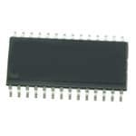
| 供应商器件封装 | 28-SOIC W |
| 其它名称 | IRS2336DSTRPBFDKR |
| 包装 | Digi-Reel® |
| 商标 | International Rectifier |
| 安装类型 | 表面贴装 |
| 安装风格 | SMD/SMT |
| 封装 | Reel |
| 封装/外壳 | 28-SOIC(0.295",7.50mm 宽) |
| 封装/箱体 | SOIC-28 Wide |
| 工作温度 | -40°C ~ 125°C |
| 工厂包装数量 | 1000 |
| 延迟时间 | 530ns |
| 最大关闭延迟时间 | 530 ns |
| 最大功率耗散 | 1.6 W |
| 最大工作温度 | + 125 C |
| 最大开启延迟时间 | 530 ns |
| 最小工作温度 | - 40 C |
| 标准包装 | 1 |
| 激励器数量 | 6 Driver |
| 电压-电源 | 10 V ~ 20 V |
| 电流-峰值 | 200mA |
| 电源电压-最大 | 20 V |
| 电源电压-最小 | 10 V |
| 类型 | High and Low Side |
| 输入类型 | 反相 |
| 输出数 | 6 |
| 输出电流 | 200 mA |
| 输出端数量 | 6 |
| 配置 | 3 相桥 |
| 配置数 | 1 |
| 高压侧电压-最大值(自举) | 600V |


- 商务部:美国ITC正式对集成电路等产品启动337调查
- 曝三星4nm工艺存在良率问题 高通将骁龙8 Gen1或转产台积电
- 太阳诱电将投资9.5亿元在常州建新厂生产MLCC 预计2023年完工
- 英特尔发布欧洲新工厂建设计划 深化IDM 2.0 战略
- 台积电先进制程称霸业界 有大客户加持明年业绩稳了
- 达到5530亿美元!SIA预计今年全球半导体销售额将创下新高
- 英特尔拟将自动驾驶子公司Mobileye上市 估值或超500亿美元
- 三星加码芯片和SET,合并消费电子和移动部门,撤换高东真等 CEO
- 三星电子宣布重大人事变动 还合并消费电子和移动部门
- 海关总署:前11个月进口集成电路产品价值2.52万亿元 增长14.8%


PDF Datasheet 数据手册内容提取
IRS2336(S)(J)PBF is not recommended for new designs. For new designs we recommend IR2136(S)(J)PBF or 6EDL04I06NT April 26, 2011 IRS2336(D) IRS23364D HIGH VOLTAGE 3 PHASE GATE DRIVER IC Features Product Summary • Drives up to six IGBT/MOSFET power devices Topology 3 Phase • Gate drive supplies up to 20 V per channel • Integrated bootstrap functionality (IRS2336(4)D) V ≤ 600 V OFFSET • Over-current protection • Over-temperature shutdown input IRS2336(D) 10 V – 20 V V • Advanced input filter OUT IRS23364D 11.5 V – 20 V • Integrated deadtime protection • Shoot-through (cross-conduction) protection Io+ & I o- (typical) 200 mA & 350 mA • Undervoltage lockout for V & V CC BS t & t (typical) 530 ns & 530 ns • Enable/disable input and fault reporting ON OFF • Adjustable fault clear timing Deadtime (typical) 275 ns • Separate logic and power grounds • 3.3 V input logic compatible Package Options • Tolerant to negative transient voltage • Designed for use with bootstrap power supplies • Matched propagation delays for all channels • -40°C to 125°C operating range • RoHS compliant • Lead-Free 28-Lead PDIP 28-Lead SOIC Wide Body Typical Applications • Appliance motor drives • Servo drives 48-Lead MLPQ7X7 44-Lead PLCC • Micro inverter drives (without 14 leads) (without 12 leads) • General purpose three phase inverters Typical Connection Diagram www.irf.com © 2009 International Rectifier
IRS2336(S)(J)PBF is not recommended for new designs. For new designs we recommend IR2136(S)(J)PBF or 6EDL04I06NT IRS2336x(D) Family Table of Contents Page Description 3 Feature Comparison 3 Simplified Block Diagram 4 Typical Application Diagram 4 Qualification Information 5 Absolute Maximum Ratings 6 Recommended Operating Conditions 7 Static Electrical Characteristics 8-9 Dynamic Electrical Characteristics 10 Functional Block Diagram 11-12 Input/Output Pin Equivalent Circuit Diagram 13-14 Lead Definitions 15-16 Lead Assignments 17 Application Information and Additional Details 18-35 Parameter Temperature Trends 36-39 Package Details 40-43 Tape and Reel Details 44-46 Part Marking Information 47 Ordering Information 48 www.irf.com © 2009 International Rectifier 2
IRS2336(S)(J)PBF is not recommended for new designs. For new designs we recommend IR2136(S)(J)PBF or 6EDL04I06NT IRS2336x(D) Family Description The IRS2336xD are high voltage, high speed, power MOSFET and IGBT gate drivers with three high-side and three low-side referenced output channels for 3-phase applications. This IC is designed to be used with low-cost bootstrap power supplies; the bootstrap diode functionality has been integrated into this device to reduce the component count and the PCB size. Proprietary HVIC and latch immune CMOS technologies have been implemented in a rugged monolithic structure. The floating logic input is compatible with standard CMOS or LSTTL outputs (down to 3.3 V logic). A current trip function which terminates all six outputs can be derived from an external current sense resistor. Enable functionality is available to terminate all six outputs simultaneously. An open-drain FAULT signal is provided to indicate that a fault (e.g., over-current, over-temperature, or undervoltage shutdown event) has occurred. Fault conditions are cleared automatically after a delay programmed externally via an RC network connected to the RCIN input. The output drivers feature a high-pulse current buffer stage designed for minimum driver cross-conduction. Shoot-through protection circuitry and a minimum deadtime circuitry have been integrated into this IC. Propagation delays are matched to simplify the HVIC’s use in high frequency applications. The floating channels can be used to drive N-channel power MOSFETs or IGBTs in the high-side configuration, which operate up to 600 V. Feature Comparison: IRS2336xD Family Part Number Input Logic UVLO V t , t V IT,TH ON OFF OUT IRS2336(D) HIN/N, LIN/N 8.9 V/ 8.2 V 0.46 V 530 ns, 530 ns 10 V – 20 V IRS23364D HIN, LIN 11.1 V/ 10.9 V 0.46 V 530 ns, 530 ns 11.5 V – 20 V www.irf.com © 2009 International Rectifier 3
IRS2336(S)(J)PBF is not recommended for new designs. For new designs we recommend IR2136(S)(J)PBF or 6EDL04I06NT IRS2336x(D) Family Simplified Block Diagram Typical Application Diagram DC Bus ≤ 600 V + Input To Voltage Load - IRS2336xD V CC Control Inputs, EN, & FAULT www.irf.com © 2009 International Rectifier 4
IRS2336(S)(J)PBF is not recommended for new designs. For new designs we recommend IR2136(S)(J)PBF or 6EDL04I06NT IRS2336x(D) Family Qualification Information† Industrial†† Qualification Level Comments: This family of ICs has passed JEDEC’s Industrial qualification. IR’s Consumer qualification level is granted by extension of the higher Industrial level. SOIC28W MSL3†††, 260°C MLPQ7X7 (per IPC/JEDEC J-STD-020) Moisture Sensitivity Level MSL3†††, 245°C PLCC44 (per IPC/JEDEC J-STD-020) Not applicable PDIP28 (non-surface mount package style) Class 1C Human Body Model (per JEDEC standard JESD22-A114) Class B ESD Machine Model (per EIA/JEDEC standard EIA/JESD22-A115) Class IV Charged Device Model †††† (per JEDEC standard JESD22-C101) Class I, Level A IC Latch-Up Test (per JESD78) RoHS Compliant Yes † Qualification standards can be found at International Rectifier’s web site http://www.irf.com/ †† Higher qualification ratings may be available should the user have such requirements. Please contact your International Rectifier sales representative for further information. ††† Higher MSL ratings may be available for the specific package types listed here. Please contact your International Rectifier sales representative for further information. †††† Charged Device Model classification is based on SOIC28W package. www.irf.com © 2009 International Rectifier 5
IRS2336(S)(J)PBF is not recommended for new designs. For new designs we recommend IR2136(S)(J)PBF or 6EDL04I06NT IRS2336x(D) Family Absolute Maximum Ratings Absolute maximum ratings indicate sustained limits beyond which damage to the device may occur. All voltage parameters are absolute voltages referenced to V unless otherwise stated in the table. The thermal resistance and SS power dissipation ratings are measured under board mounted and still air conditions. Voltage clamps are included between V & COM (25 V), V & V (20 V), and V & V (20 V). CC CC SS B S Symbol Definition Min Max Units V Low side supply voltage -0.3 20† CC IRS2336(D) V -0.3 V +5.2 V Logic input voltage (HIN, LIN, ITRIP, EN) SS SS IN IRS23364D V -0.3 V +0.3 SS CC V RCIN input voltage V -0.3 V +0.3 RCIN SS CC V High-side floating well supply voltage -0.3 620† B V V High-side floating well supply return voltage V -20† V +0.3 S B B V Floating gate drive output voltage V -0.3 V +0.3 HO S B V Low-side output voltage COM-0.3 V +0.3 LO CC V Fault output voltage V -0.3 V +0.3 FLT SS CC COM Power ground V -25 V +0.3 CC CC dV /dt Allowable V offset supply transient relative to V — 50 V/ns S S SS PW High-side input pulse width 500 — ns HIN 28-Lead PDIP — 1.5 28-Lead — 1.6 SOICW PD Package power dissipation @ TA ≤+25ºC 44-Lead PLCC — 2.0 W 48-Lead — 2.0 MLPQ7X7 28-Lead PDIP — 83 28-Lead — 78 SOICW RthJA Thermal resistance, junction to ambient 44-Lead PLCC — 63 ºC/W 48-Lead — 63 MLPQ7X7 T Junction temperature — 150 J T Storage temperature -55 150 ºC S T Lead temperature (soldering, 10 seconds) — 300 L † All supplies are tested at 25 V. An internal 20 V clamp exists for each supply. www.irf.com © 2009 International Rectifier 6
IRS2336(S)(J)PBF is not recommended for new designs. For new designs we recommend IR2136(S)(J)PBF or 6EDL04I06NT IRS2336x(D) Family Recommended Operating Conditions For proper operation, the device should be used within the recommended conditions. All voltage parameters are absolute voltages referenced to V unless otherwise stated in the table. The offset rating is tested with supplies of SS (V -COM) = (V -V ) = 15 V. CC B S Symbol Definition Min Max Units IRS2336(D) 10 20 V Low-side supply voltage CC IRS23364D 11.5 20 IRS2336(D) V +5 V HIN, LIN, & EN input voltage V SS IN IRS23364D SS V CC IRS2336(D) V +10 V +20 V High-side floating well supply voltage S S B IRS23364D V +11.5 V +20 S S V High-side floating well supply offset voltage† COM-8 600 S V V (t) Transient high-side floating supply voltage†† -50 600 S V Floating gate drive output voltage V V HO s B V Low-side output voltage COM V LO CC COM Power ground -5 5 V FAULT output voltage V V FLT SS CC V RCIN input voltage V V RCIN SS CC V ITRIP input voltage V V +5 ITRIP SS SS T Ambient temperature -40 125 ºC A † Logic operation for VS of –8 V to 600 V. Logic state held for VS of –8 V to –VBS. Please refer to Design Tip DT97-3 for more details. †† Operational for transient negative VS of VSS - 50 V with a 50 ns pulse width. Guaranteed by design. Refer to the Application Information section of this datasheet for more details. www.irf.com © 2009 International Rectifier 7
IRS2336(S)(J)PBF is not recommended for new designs. For new designs we recommend IR2136(S)(J)PBF or 6EDL04I06NT IRS2336x(D) Family Static Electrical Characteristics (V -COM) = (V -V ) = 15 V. T = 25oC unless otherwise specified. The V and I parameters are referenced to V CC B S A IN IN SS and are applicable to all six channels. The V and I parameters are referenced to respective V and COM and are O O S applicable to the respective output leads HO or LO. The V parameters are referenced to V . The V CCUV SS BSUV parameters are referenced to V . S Symbol Definition Min Typ Max Units Test Conditions V supply undervoltage positive IRS2336(D) 8 8.9 9.8 V CC CCUV+ going threshold IRS23364D 10.4 11.1 11.6 V supply undervoltage negative IRS2336(D) 7.4 8.2 9 V CC CCUV- going threshold IRS23364D 10.2 10.9 11.4 V supply undervoltage IRS2336(D) 0.3 0.7 — V CC CCUVHY hysteresis IRS23364D — 0.2 — V NA V supply undervoltage positive IRS2336(D) 8 8.9 9.8 V BS BSUV+ going threshold IRS23364D 10.4 11.1 11.6 V supply undervoltage negative IRS2336(D) 7.4 8.2 9 V BS BSUV- going threshold IRS23364D 10.2 10.9 11.4 V supply undervoltage IRS2336(D) 0.3 0.7 — V BS BSUVHY hysteresis IRS23364D — 0.2 — I High-side floating well offset supply leakage — — 50 V = V = 600 V LK µA B S I Quiescent V supply current — 70 120 QBS BS All inputs are in the IRS2336 — 2 3 I Quiescent V supply current mA off state QCC CC IR2336(4)D — 3 4 V High level output voltage drop, V -V — 0.90 1.4 V OH BIAS O I = 20 mA V Low level output voltage drop, V — 0.40 0.6 V O OL O V =0 V,V =0 V, I Output high short circuit pulsed current 120 200 — O IN o+ PW ≤ 10 µs mA V =15 V,V =5 V, I Output low short circuit pulsed current 250 350 — O IN o- PW ≤ 10 µs Logic “0” input voltage V 2.5 — — IH Logic “1” input voltage NA Logic “1” input voltage V — — 0.8 V IL Logic “0” input voltage Input voltage clamp V IRS2336(D) 4.8 5.2 5.65 I = 100 µA IN,CLAMP (HIN, LIN, ITRIP and EN) IN IRS2336(D) — 150 200 V = 0 V I Input bias current (HO = High) IN HIN+ IRS23364D — 120 165 V = 4 V IRS2336(D) — 110 150 IN I Input bias current (HO = Low) HIN- IRS23364D — — 1 µA V = 0 V IRS2336(D) — 150 200 IN I Input bias current (LO = High) LIN+ IRS23364D — 120 165 V = 4 V IRS2336(D) — 110 150 IN I Input bias current (LO = Low) LIN- IRS23364D — — 1 V = 0 V IN V RCIN positive going threshold — 8 — RCIN,TH V NA V RCIN hysteresis — 3 — RCIN,HY I RCIN input bias current — — 1 µA V = 0 V or 15 V RCIN RCIN R RCIN low on resistance — 50 100 Ω I = 1.5 mA ON,RCIN www.irf.com © 2009 International Rectifier 8
IRS2336(S)(J)PBF is not recommended for new designs. For new designs we recommend IR2136(S)(J)PBF or 6EDL04I06NT IRS2336x(D) Family Static Electrical Characteristics (continued) Symbol Definition Min Typ Max Units Test Conditions V ITRIP positive going threshold 0.37 0.46 0.55 IT,TH+ — — VIT,TH- ITRIP negative going threshold 0.4 V NA — — V ITRIP hysteresis 0.07 IT,HYS IRS2336(D) — 5 20 I “High” ITRIP input bias current V = 4 V ITRIP+ IRS23364D — 5 40 µA IN — — I “Low” ITRIP input bias current 1 V = 0 V ITRIP- IN — — VEN,TH+ Enable positive going threshold 2.5 V NA V Enable negative going threshold 0.8 — — EN,TH- IRS2336(D) — 5 20 I “High” enable input bias current V = 4 V EN+ IRS23364D — 120 165 µA IN I “Low” enable input bias current — — 1 V = 0 V EN- IN — R FAULT low on resistance 50 100 I = 1.5 mA ON,FLT Ω R Internal BS diode Ron (IRS2336(4)D) — 200 — NA BS www.irf.com © 2009 International Rectifier 9
IRS2336(S)(J)PBF is not recommended for new designs. For new designs we recommend IR2136(S)(J)PBF or 6EDL04I06NT IRS2336x(D) Family Dynamic Electrical Characteristics V = V = 15 V, V = V = COM, T = 25oC, and C = 1000 pF unless otherwise specified. CC B S SS A L Symbol Definition Min Typ Max Units Test Conditions t Turn-on propagation delay 400 530 750 ON t Turn-off propagation delay 400 530 750 OFF t Turn-on rise time — 125 190 R V = 0 V & 5 V t Turn-off fall time — 50 75 IN F Input filter time† ns tFIL,IN (HIN, LIN, ITRIP) 200 350 510 Enable low to output shutdown t 350 460 650 V V = 0 V or 5 V EN propagation delay IN, EN t Enable input filter time 100 200 — NA FILTER,EN FAULT clear time V = 0 V or 5 V t 1.3 1.65 2 ms IN FLTCLR RCIN: R = 2 MΩ, C = 1 nF V = 0 V ITRIP ITRIP to output shutdown t 500 750 1200 V = 5 V ITRIP propagation delay ITRIP t ITRIP blanking time — 400 — V = 0 V or 5 V BL IN t ITRIP to FAULT propagation delay 400 600 950 V = 5 V FLT ITRIP DT Deadtime 190 275 420 ns V = 0 V & 5 V without IN MDT DT matching†† — — 60 external deadtime MT Delay matching time (t , t ) †† — — 50 VIN = 0 V & 5 V with external ON OFF deadtime larger than DT PM Pulse width distortion††† — — 75 PW input=10 µs † The minimum width of the input pulse is recommended to exceed 500 ns to ensure the filtering time of the input filter is exceeded. †† This parameter applies to all of the channels. Please see the application section for more details. ††† PM is defined as PW - PW . IN OUT www.irf.com © 2009 International Rectifier 10
IRS2336(S)(J)PBF is not recommended for new designs. For new designs we recommend IR2136(S)(J)PBF or 6EDL04I06NT IRS2336x(D) Family Functional Block Diagram: IRS2336(D) Note: IRS2336 is without the “Integrated BootFET” www.irf.com © 2009 International Rectifier 11
IRS2336(S)(J)PBF is not recommended for new designs. For new designs we recommend IR2136(S)(J)PBF or 6EDL04I06NT IRS2336x(D) Family Functional Block Diagram: IRS23364D www.irf.com © 2009 International Rectifier 12
IRS2336(S)(J)PBF is not recommended for new designs. For new designs we recommend IR2136(S)(J)PBF or 6EDL04I06NT IRS2336x(D) Family Input/Output Pin Equivalent Circuit Diagrams: IRS2336(D) www.irf.com © 2009 International Rectifier 13
IRS2336(S)(J)PBF is not recommended for new designs. For new designs we recommend IR2136(S)(J)PBF or 6EDL04I06NT IRS2336x(D) Family Input/Output Pin Equivalent Circuit Diagrams: IRS23364D www.irf.com © 2009 International Rectifier 14
IRS2336(S)(J)PBF is not recommended for new designs. For new designs we recommend IR2136(S)(J)PBF or 6EDL04I06NT IRS2336x(D) Family Lead Definitions: IRS2336(D) Symbol Description VCC Low-side supply voltage VSS Logic ground VB1 High-side gate drive floating supply (phase 1) VB2 High-side gate drive floating supply (phase 2) VB3 High-side gate drive floating supply (phase 3) VS1 High voltage floating supply return (phase 1) VS2 High voltage floating supply return (phase 2) VS3 High voltage floating supply return (phase 3) HIN1/N Logic inputs for high-side gate driver outputs (phase 1); input is out-of-phase with output HIN2/N Logic inputs for high-side gate driver outputs (phase 2); input is out-of-phase with output HIN3/N Logic inputs for high-side gate driver outputs (phase 3); input is out-of-phase with output LIN1/N Logic inputs for low-side gate driver outputs (phase 1); input is out-of-phase with output LIN2/N Logic inputs for low-side gate driver outputs (phase 2); input is out-of-phase with output LIN3/N Logic inputs for low-side gate driver outputs (phase 3); input is out-of-phase with output HO1 High-side driver outputs (phase 1) HO2 High-side driver outputs (phase 2) HO3 High-side driver outputs (phase 3) LO1 Low-side driver outputs (phase 1) LO2 Low-side driver outputs (phase 2) LO3 Low-side driver outputs (phase 3) COM Low-side gate drive return Indicates over-current, over-temperature (ITRIP), or low-side undervoltage lockout has occurred. FAULT/N This pin has negative logic and an open-drain output. The use of over-current and over- temperature protection requires the use of external components. Logic input to shutdown functionality. Logic functions when EN is high (i.e., positive logic). No EN effect on FAULT and not latched. Analog input for over-current shutdown. When active, ITRIP shuts down outputs and activates ITRIP FAULT and RCIN low. When ITRIP becomes inactive, FAULT stays active low for an externally set time t , then automatically becomes inactive (open-drain high impedance). FLTCLR An external RC network input used to define the FAULT CLEAR delay (t )approximately FLTCLR RCIN equal to R*C. When RCIN > 8 V, the FAULT pin goes back into an open-drain high-impedance state. www.irf.com © 2009 International Rectifier 15
IRS2336(S)(J)PBF is not recommended for new designs. For new designs we recommend IR2136(S)(J)PBF or 6EDL04I06NT IRS2336x(D) Family Lead Definitions: IRS23364D Symbol Description VCC Low-side supply voltage VSS Logic ground VB1 High-side gate drive floating supply (phase 1) VB2 High-side gate drive floating supply (phase 2) VB3 High-side gate drive floating supply (phase 3) VS1 High voltage floating supply return (phase 1) VS2 High voltage floating supply return (phase 2) VS3 High voltage floating supply return (phase 3) HIN1 Logic inputs for high-side gate driver outputs (phase 1); input is in-phase with output HIN2 Logic inputs for high-side gate driver outputs (phase 2); input is in-phase with output HIN3 Logic inputs for high-side gate driver outputs (phase 3); input is in-phase with output LIN1 Logic inputs for low-side gate driver outputs (phase 1); input is in-phase with output LIN2 Logic inputs for low-side gate driver outputs (phase 2); input is in-phase with output LIN3 Logic inputs for low-side gate driver outputs (phase 3); input is in-phase with output HO1 High-side driver outputs (phase 1) HO2 High-side driver outputs (phase 2) HO3 High-side driver outputs (phase 3) LO1 Low-side driver outputs (phase 1) LO2 Low-side driver outputs (phase 2) LO3 Low-side driver outputs (phase 3) COM Low-side gate drive return Indicates over-current, over-temperature (ITRIP), or low-side undervoltage lockout has occurred. FAULT/N This pin has negative logic and an open-drain output. The use of over-current and over- temperature protection requires the use of external components. Logic input to shutdown functionality. Logic functions when EN is high (i.e., positive logic). No EN effect on FAULT and not latched. Analog input for over-current shutdown. When active, ITRIP shuts down outputs and activates ITRIP FAULT and RCIN low. When ITRIP becomes inactive, FAULT stays active low for an externally set time t , then automatically becomes inactive (open-drain high impedance). FLTCLR An external RC network input used to define the FAULT CLEAR delay (t )approximately FLTCLR RCIN equal to R*C. When RCIN > 8 V, the FAULT pin goes back into an open-drain high-impedance state. www.irf.com © 2009 International Rectifier 16
IRS2336(S)(J)PBF is not recommended for new designs. For new designs we recommend IR2136(S)(J)PBF or 6EDL04I06NT IRS2336x(D) Family Lead Assignments IRS2336(D) VB2 HO2 VS2 VB3 HO3 VS3 34 33 32 31 30 29 VS1 1 28 n.c. HO1 2 27 n.c. VB1 3 26 n.c. 34 Lead 25 LO1 24 LO2 MLPQ VCC 4 23 LO3 HIN1 5 22 COM HIN2 6 21 n.c. HIN3 7 20 VSS n.c. 8 19 n.c. 9 10 11 12 13 14 15 16 17 18 LIN1 LIN2 LIN3 n.c. FAULT n.c. ITRIP EN RCIN n.c. www.irf.com © 2009 International Rectifier 17
IRS2336(S)(J)PBF is not recommended for new designs. For new designs we recommend IR2136(S)(J)PBF or 6EDL04I06NT IRS2336x(D) Family Application Information and Additional Details Information regarding the following topics are included as subsections within this section of the datasheet. • IGBT/MOSFET Gate Drive • Switching and Timing Relationships • Deadtime • Matched Propagation Delays • Input Logic Compatibility • Undervoltage Lockout Protection • Shoot-Through Protection • Enable Input • Fault Reporting and Programmable Fault Clear Timer • Over-Current Protection • Over-Temperature Shutdown Protection • Truth Table: Undervoltage lockout, ITRIP, and ENABLE • Advanced Input Filter • Short-Pulse / Noise Rejection • Integrated Bootstrap Functionality • Bootstrap Power Supply Design • Separate Logic and Power Grounds • Tolerant to Negative V Transients S • PCB Layout Tips • Integrated Bootstrap FET limitation • Additional Documentation IGBT/MOSFET Gate Drive The IRS2336xD HVICs are designed to drive up to six MOSFET or IGBT power devices. Figures 1 and 2 illustrate several parameters associated with the gate drive functionality of the HVIC. The output current of the HVIC, used to drive the gate of the power switch, is defined as I . The voltage that drives the gate of the external power switch is O defined as V for the high-side power switch and V for the low-side power switch; this parameter is sometimes HO LO generically called V and in this case does not differentiate between the high-side or low-side output voltage. OUT V V B B (or V ) (or V ) CC CC I O+ HO HO (or LO) (or LO) + I O- V (or V ) HO LO - V V S S (or COM) (or COM) Figure 1: HVIC sourcing current Figure 2: HVIC sinking current www.irf.com © 2009 International Rectifier 18
IRS2336(S)(J)PBF is not recommended for new designs. For new designs we recommend IR2136(S)(J)PBF or 6EDL04I06NT IRS2336x(D) Family Switching and Timing Relationships The relationship between the input and output signals of the IRS2336(D) and IRS23364D are illustrated below in Figures 3 and 4. From these figures, we can see the definitions of several timing parameters (i.e., PW , PW , t , IN OUT ON t , t , and t ) associated with this device. OFF R F LINx LINx (or HINx) 50% 50% (or HINx) 50% 50% PWIN PWIN tON tR tOFF tF tON tR tOFF tF PWOUT PWOUT 90% 90% 90% 90% LOx LOx (or HOx) (or HOx) 10% 10% 10% 10% Figure 3: Switching time waveforms (IRS2336(D)) Figure 4: Switching time waveforms (IRS23364D) The following two figures illustrate the timing relationships of some of the functionality of the IRS2336xD; this functionality is described in further detail later in this document. During interval A of Figure 5, the HVIC has received the command to turn-on both the high- and low-side switches at the same time; as a result, the shoot-through protection of the HVIC has prevented this condition and both the high- and low-side output are held in the off state. Interval B of Figures 5 and 6 shows that the signal on the ITRIP input pin has gone from a low to a high state; as a result, all of the gate drive outputs have been disabled (i.e., see that HOx has returned to the low state; LOx is also held low), the voltage on the RCIN pin has been pulled to 0 V, and a fault is reported by the FAULT output transitioning to the low state. Once the ITRIP input has returned to the low state, the output will remain disabled and the fault condition reported until the voltage on the RCIN pin charges up to V (see interval C in Figure 6); the RCIN,TH charging characteristics are dictated by the RC network attached to the RCIN pin. During intervals D and E of Figure 5, we can see that the enable (EN) pin has been pulled low (as is the case when the driver IC has received a command from the control IC to shutdown); this results in the outputs (HOx and LOx) being held in the low state until the enable pin is pulled high. www.irf.com © 2009 International Rectifier 19
IRS2336(S)(J)PBF is not recommended for new designs. For new designs we recommend IR2136(S)(J)PBF or 6EDL04I06NT IRS2336x(D) Family Figure 5: Input/output timing diagram for the IRS2336xD family Interval B Interval C VIT,TH+ VIT,TH- ITRIP FAULT tFLT 50% 50% RCIN VRCIN,TH HOx 90% tFLTCLR tITRIP Figure 6: Detailed view of B & C intervals Deadtime This family of HVICs features integrated deadtime protection circuitry. The deadtime for these ICs is fixed; other ICs within IR’s HVIC portfolio feature programmable deadtime for greater design flexibility. The deadtime feature inserts a time period (a minimum deadtime) in which both the high- and low-side power switches are held off; this is done to ensure that the power switch being turned off has fully turned off before the second power switch is turned on. This minimum deadtime is automatically inserted whenever the external deadtime is shorter than DT; external deadtimes larger than DT are not modified by the gate driver. Figure 7 illustrates the deadtime period and the relationship between the output gate signals. The deadtime circuitry of the IRS2336xD is matched with respect to the high- and low-side outputs of a given channel; additionally, the deadtimes of each of the three channels are matched. Figure 7 defines the two deadtime parameters (i.e., DT and DT ) of a specific channel; the deadtime matching parameter (MDT) associated with the 1 2 IRS2336xD specifies the maximum difference between DT and DT . The MDT parameter also applies when 1 2 comparing the DT of one channel of the IRS2336xD to that of another. www.irf.com © 2009 International Rectifier 20
IRS2336(S)(J)PBF is not recommended for new designs. For new designs we recommend IR2136(S)(J)PBF or 6EDL04I06NT IRS2336x(D) Family Figure 7: Illustration of deadtime Matched Propagation Delays The IRS2336xD family of HVICs is designed with propagation delay matching circuitry. With this feature, the IC’s response at the output to a signal at the input requires approximately the same time duration (i.e., t , t ) for both ON OFF the low-side channels and the high-side channels; the maximum difference is specified by the delay matching parameter (MT). Additionally, the propagation delay for each low-side channel is matched when compared to the other low-side channels and the propagation delays of the high-side channels are matched with each other; the MT specification applies as well. The propagation turn-on delay (t ) of the IRS2336xD is matched to the propagation ON turn-on delay (t ). OFF Input Logic Compatibility The inputs of this IC are compatible with standard CMOS and TTL outputs. The IRS2336xD family has been designed to be compatible with 3.3 V and 5 V logic-level signals. The IRS2336(D) features an integrated 5.2 V Zener clamp on the HIN, LIN, ITRIP, and EN pins; the IRS23364D does not offer this input clamp. Figure 8 illustrates an input signal to the IRS2336(D) and IRS23364D, its input threshold values, and the logic state of the IC as a result of the input signal. Figure 8: HIN & LIN input thresholds www.irf.com © 2009 International Rectifier 21
IRS2336(S)(J)PBF is not recommended for new designs. For new designs we recommend IR2136(S)(J)PBF or 6EDL04I06NT IRS2336x(D) Family Undervoltage Lockout Protection This family of ICs provides undervoltage lockout protection on both the V (logic and low-side circuitry) power supply CC and the V (high-side circuitry) power supply. Figure 9 is used to illustrate this concept; V (or V ) is plotted over BS CC BS time and as the waveform crosses the UVLO threshold (V or V ) the undervoltage protection is enabled or CCUV+/- BSUV+/- disabled. Upon power-up, should the V voltage fail to reach the V threshold, the IC will not turn-on. Additionally, if the CC CCUV+ V voltage decreases below the V threshold during operation, the undervoltage lockout circuitry will recognize a CC CCUV- fault condition and shutdown the high- and low-side gate drive outputs, and the FAULT pin will transition to the low state to inform the controller of the fault condition. Upon power-up, should the V voltage fail to reach the V threshold, the IC will not turn-on. Additionally, if the V BS BSUV BS voltage decreases below the V threshold during operation, the undervoltage lockout circuitry will recognize a fault BSUV condition, and shutdown the high-side gate drive outputs of the IC. The UVLO protection ensures that the IC drives the external power devices only when the gate supply voltage is sufficient to fully enhance the power devices. Without this feature, the gates of the external power switch could be driven with a low voltage, resulting in the power switch conducting current while the channel impedance is high; this could result in very high conduction losses within the power device and could lead to power device failure. Figure 9: UVLO protection Shoot-Through Protection The IRS2336xD family of high-voltage ICs is equipped with shoot-through protection circuitry (also known as cross- conduction prevention circuitry). Figure 10 shows how this protection circuitry prevents both the high- and low-side switches from conducting at the same time. Table 1 illustrates the input/output relationship of the devices in the form of a truth table. Note that the IRS2336(D) has inverting inputs (the output is out-of-phase with its respective input) while the IRS23364D has non-inverting inputs (the output is in-phase with its respective input). www.irf.com © 2009 International Rectifier 22
IRS2336(S)(J)PBF is not recommended for new designs. For new designs we recommend IR2136(S)(J)PBF or 6EDL04I06NT IRS2336x(D) Family Figure 10: Illustration of shoot-through protection circuitry IRS2336(D) IRS23364D HIN LIN HO LO HIN LIN HO LO 0 0 0 0 0 0 0 0 0 1 1 0 0 1 0 1 1 0 0 1 1 0 1 0 1 1 0 0 1 1 0 0 Table 1: Input/output truth table for IRS2336D and IRS23364D Enable Input The IRS2336xD family of HVICs is equipped with an enable input pin that is used to shutdown or enable the HVIC. When the EN pin is in the high state the HVIC is able to operate normally (assuming no other fault conditions). When a condition occurs that should shutdown the HVIC, the EN pin should see a low logic state. The enable circuitry of the IRS2336xD features an input filter; the minimum input duration is specified by t . Please refer to the EN FILTER,EN pin parameters V , V , and I for the details of its use. Table 2 gives a summary of this pin’s functionality EN,TH+ EN,TH- EN and Figure 11 illustrates the outputs’ response to a shutdown command. EN VEN,TH- Enable Input tEN Enable input high Outputs enabled* Enable input low Outputs disabled HOx 90% (or LOx) Table 2: Enable functionality truth table Figure 11: Output enable timing waveform (*assumes no other fault condition) www.irf.com © 2009 International Rectifier 23
IRS2336(S)(J)PBF is not recommended for new designs. For new designs we recommend IR2136(S)(J)PBF or 6EDL04I06NT IRS2336x(D) Family Fault Reporting and Programmable Fault Clear Timer The IRS2336xD family provides an integrated fault reporting output and an adjustable fault clear timer. There are two situations that would cause the HVIC to report a fault via the FAULT pin. The first is an undervoltage condition of V CC and the second is if the ITRIP pin recognizes a fault. Once the fault condition occurs, the FAULT pin is internally pulled to V and the fault clear timer is activated. The fault output stays in the low state until the fault condition has SS been removed and the fault clear timer expires; once the fault clear timer expires, the voltage on the FAULT pin will return to V . CC The length of the fault clear time period (t ) is determined by exponential charging characteristics of the capacitor FLTCLR where the time constant is set by R and C . In Figure 12 where we see that a fault condition has occurred RCIN RCIN (UVLO or ITRIP), RCIN and FAULT are pulled to V , and once the fault has been removed, the fault clear timer SS begins. Figure 13 shows that R is connected between the V and the RCIN pin, while C is placed between RCIN CC RCIN the RCIN and V pins. SS Figure 12: RCIN and FAULT pin waveforms Figure 13: Programming the fault clear timer The design guidelines for this network are shown in Table 3. ≤1 nF C RCIN Ceramic 0.5 MΩ to 2 MΩ R RCIN >> R ON,RCIN Table 3: Design guidelines The length of the fault clear time period can be determined by using the formula below. v (t) = V(1-e-t/RC) C f t = -(R C )ln(1-V /V ) FLTCLR RCIN RCIN RCIN,TH CC www.irf.com © 2009 International Rectifier 24
IRS2336(S)(J)PBF is not recommended for new designs. For new designs we recommend IR2136(S)(J)PBF or 6EDL04I06NT IRS2336x(D) Family Over-Current Protection The IRS2336xD HVICs are equipped with an ITRIP input pin. This functionality can be used to detect over-current events in the DC- bus. Once the HVIC detects an over-current event through the ITRIP pin, the outputs are shutdown, a fault is reported through the FAULT pin, and RCIN is pulled to V . SS The level of current at which the over-current protection is initiated is determined by the resistor network (i.e., R , R , 0 1 and R ) connected to ITRIP as shown in Figure 14, and the ITRIP threshold (V ). The circuit designer will need to 2 IT,TH+ determine the maximum allowable level of current in the DC- bus and select R , R , and R such that the voltage at 0 1 2 node V reaches the over-current threshold (V ) at that current level. X IT,TH+ V = R I (R /(R +R )) IT,TH+ 0DC- 1 1 2 Figure 14: Programming the over-current protection For example, a typical value for resistor R could be 50 mΩ. The voltage of the ITRIP pin should not be allowed to 0 exceed 5 V; if necessary, an external voltage clamp may be used. Over-Temperature Shutdown Protection The ITRIP input of the IRS2336xD can also be used to detect over-temperature events in the system and initiate a shutdown of the HVIC (and power switches) at that time. In order to use this functionality, the circuit designer will need to design the resistor network as shown in Figure 15 and select the maximum allowable temperature. This network consists of a thermistor and two standard resistors R and R . As the temperature changes, the 3 4 resistance of the thermistor will change; this will result in a change of voltage at node V . The resistor values should X be selected such the voltage V should reach the threshold voltage (V ) of the ITRIP functionality by the time that X IT,TH+ the maximum allowable temperature is reached. The voltage of the ITRIP pin should not be allowed to exceed 5 V. When using both the over-current protection and over-temperature protection with the ITRIP input, OR-ing diodes (e.g., DL4148) can be used. This network is shown in Figure 16; the OR-ing diodes have been labeled D and D . 1 2 www.irf.com © 2009 International Rectifier 25
IRS2336(S)(J)PBF is not recommended for new designs. For new designs we recommend IR2136(S)(J)PBF or 6EDL04I06NT IRS2336x(D) Family Figure 15: Programming over-temperature protection Figure 16: Using over-current protection and over- temperature protection Truth Table: Undervoltage lockout, ITRIP, and ENABLE Table 4 provides the truth table for the IRS2336xD. The first line shows that the UVLO for V has been tripped; the CC FAULT output has gone low and the gate drive outputs have been disabled. V is not latched in this case and CCUV when V is greater than V , the FAULT output returns to the high impedance state. CC CCUV The second case shows that the UVLO for V has been tripped and that the high-side gate drive outputs have been BS disabled. After V exceeds the V threshold, HO will stay low until the HVIC input receives a new falling BS BSUV (IRS2336(D)) or rising (IRS23364D) transition of HIN. The third case shows the normal operation of the HVIC. The fourth case illustrates that the ITRIP trip threshold has been reached and that the gate drive outputs have been disabled and a fault has been reported through the fault pin. In the last case, the HVIC has received a command through the EN input to shutdown; as a result, the gate drive outputs have been disabled. VCC VBS ITRIP EN RCIN FAULT LO HO UVLO V <V — — — High 0 0 0 CC CCUV UVLO V 15 V <V 0 V 5 V High High impedance LIN 0 BS BSUV Normal operation 15 V 15 V 0 V 5 V High High impedance LIN HIN ITRIP fault 15 V 15 V >V 5 V Low 0 0 0 ITRIP EN command 15 V 15 V 0 V 0 V High High impedance 0 0 Table 4: IRS2336xD UVLO, ITRIP, EN, RCIN, & FAULT truth table Advanced Input Filter The advanced input filter allows an improvement in the input/output pulse symmetry of the HVIC and helps to reject noise spikes and short pulses. This input filter has been applied to the HIN, LIN, and EN inputs. The working principle of the new filter is shown in Figures 17 and 18. Figure 17 shows a typical input filter and the asymmetry of the input and output. The upper pair of waveforms (Example 1) show an input signal with a duration much longer then t ; the resulting output is approximately the FIL,IN difference between the input signal and t . The lower pair of waveforms (Example 2) show an input signal with a FIL,IN duration slightly longer then t ; the resulting output is approximately the difference between the input signal and FIL,IN t . FIL,IN Figure 18 shows the advanced input filter and the symmetry between the input and output. The upper pair of waveforms (Example 1) show an input signal with a duration much longer then t ; the resulting output is FIL,IN approximately the same duration as the input signal. The lower pair of waveforms (Example 2) show an input signal with a duration slightly longer then t ; the resulting output is approximately the same duration as the input signal. FIL,IN www.irf.com © 2009 International Rectifier 26
IRS2336(S)(J)PBF is not recommended for new designs. For new designs we recommend IR2136(S)(J)PBF or 6EDL04I06NT IRS2336x(D) Family Figure 17: Typical input filter Figure 18: Advanced input filter Short-Pulse / Noise Rejection This device’s input filter provides protection against short-pulses (e.g., noise) on the input lines. If the duration of the input signal is less than t , the output will not change states. Example 1 of Figure 19 shows the input and output in FIL,IN the low state with positive noise spikes of durations less than t ; the output does not change states. Example 2 of FIL,IN Figure 19 shows the input and output in the high state with negative noise spikes of durations less than t ; the FIL,IN output does not change states. 1 e pl m a x E 2 e pl m a x E Figure 19: Noise rejecting input filters Figures 20 and 21 present lab data that illustrates the characteristics of the input filters while receiving ON and OFF pulses. The input filter characteristic is shown in Figure 20; the left side illustrates the narrow pulse ON (short positive pulse) characteristic while the left shows the narrow pulse OFF (short negative pulse) characteristic. The x-axis of Figure 20 shows the duration of PW , while the y-axis shows the resulting PW duration. It can be seen that for a PW IN OUT IN duration less than t , that the resulting PW duration is zero (e.g., the filter rejects the input signal/noise). We FIL,IN OUT also see that once the PW duration exceed t , that the PW durations mimic the PW durations very well over IN FIL,IN OUT IN this interval with the symmetry improving as the duration increases. To ensure proper operation of the HVIC, it is suggested that the input pulse width for the high-side inputs be ≥ 500 ns. The difference between the PW and PW signals of both the narrow ON and narrow OFF cases is shown in OUT IN Figure 21; the careful reader will note the scale of the y-axis. The x-axis of Figure 21 shows the duration of PW , IN while the y-axis shows the resulting PW –PW duration. This data illustrates the performance and near symmetry OUT IN of this input filter. www.irf.com © 2009 International Rectifier 27
IRS2336(S)(J)PBF is not recommended for new designs. For new designs we recommend IR2136(S)(J)PBF or 6EDL04I06NT IRS2336x(D) Family s) n e ( m Ti Figure 20: IRS2336xD input filter characteristic Figure 21: Difference between the input pulse and the output pulse Integrated Bootstrap Functionality The new IRS2336xD family features integrated high-voltage bootstrap MOSFETs that eliminate the need of the external bootstrap diodes and resistors in many applications. There is one bootstrap MOSFET for each high-side output channel and it is connected between the V supply and CC its respective floating supply (i.e., V , V , V ); see Figure 22 for an illustration of this internal connection. B1 B2 B3 The integrated bootstrap MOSFET is turned on only during the time when LO is ‘high’, and it has a limited source current due to R . The V voltage will be charged each cycle depending on the on-time of LO and the value of the BS BS C capacitor, the drain-source (collector-emitter) drop of the external IGBT (or MOSFET), and the low-side free- BS wheeling diode drop. The bootstrap MOSFET of each channel follows the state of the respective low-side output stage (i.e., the bootstrap MOSFET is ON when LO is high, it is OFF when LO is low), unless the V voltage is higher than approximately 110% B of V . In that case, the bootstrap MOSFET is designed to remain off until V returns below that threshold; this CC B concept is illustrated in Figure 23. www.irf.com © 2009 International Rectifier 28
IRS2336(S)(J)PBF is not recommended for new designs. For new designs we recommend IR2136(S)(J)PBF or 6EDL04I06NT IRS2336x(D) Family V B1 V CC V B2 V B3 Figure 22: Internal bootstrap MOSFET connection Figure 23: Bootstrap MOSFET state diagram A bootstrap MOSFET is suitable for most of the PWM modulation schemes and can be used either in parallel with the external bootstrap network (i.e., diode and resistor) or as a replacement of it. The use of the integrated bootstrap as a replacement of the external bootstrap network may have some limitations. An example of this limitation may arise when this functionality is used in non-complementary PWM schemes (typically 6-step modulations) and at very high PWM duty cycle. In these cases, superior performances can be achieved by using an external bootstrap diode in parallel with the internal bootstrap network. Bootstrap Power Supply Design For information related to the design of the bootstrap power supply while using the integrated bootstrap functionality of the IRS2336xD family, please refer to Application Note 1123 (AN-1123) entitled “Bootstrap Network Analysis: Focusing on the Integrated Bootstrap Functionality.” This application note is available at www.irf.com. For information related to the design of a standard bootstrap power supply (i.e., using an external discrete diode) please refer to Design Tip 04-4 (DT04-4) entitled “Using Monolithic High Voltage Gate Drivers.” This design tip is available at www.irf.com. Separate Logic and Power Grounds The IRS2336xD has separate logic and power ground pin (V and COM respectively) to eliminate some of the noise SS problems that can occur in power conversion applications. Current sensing shunts are commonly used in many applications for power inverter protection (i.e., over-current protection), and in the case of motor drive applications, for motor current measurements. In these situations, it is often beneficial to separate the logic and power grounds. Figure 24 shows a HVIC with separate V and COM pins and how these two grounds are used in the system. The SS V is used as the reference point for the logic and over-current circuitry; V in the figure is the voltage between the SS X ITRIP pin and the V pin. Alternatively, the COM pin is the reference point for the low-side gate drive circuitry. The SS output voltage used to drive the low-side gate is V -COM; the gate-emitter voltage (V ) of the low-side switch is the LO GE output voltage of the driver minus the drop across R . G,LO www.irf.com © 2009 International Rectifier 29
IRS2336(S)(J)PBF is not recommended for new designs. For new designs we recommend IR2136(S)(J)PBF or 6EDL04I06NT IRS2336x(D) Family DC+ BUS DBS VB VCC (x3) CBS HO (x3) RG,HO H VS V (x3) VS1 VS2 VS3 I C LO ITRIP (x3) RG,LO + + + V V V GE1 GE2 GE3 VSS COM - - - R2 R0 + VX R1 - DC-BUS Figure 24: Separate V and COM pins SS Tolerant to Negative V Transients S A common problem in today’s high-power switching converters is the transient response of the switch node’s voltage as the power switches transition on and off quickly while carrying a large current. A typical 3-phase inverter circuit is shown in Figure 25; here we define the power switches and diodes of the inverter. If the high-side switch (e.g., the IGBT Q1 in Figures 26 and 27) switches off, while the U phase current is flowing to an inductive load, a current commutation occurs from high-side switch (Q1) to the diode (D2) in parallel with the low- side switch of the same inverter leg. At the same instance, the voltage node V , swings from the positive DC bus S1 voltage to the negative DC bus voltage. Figure 25: Three phase inverter www.irf.com © 2009 International Rectifier 30
IRS2336(S)(J)PBF is not recommended for new designs. For new designs we recommend IR2136(S)(J)PBF or 6EDL04I06NT IRS2336x(D) Family DC+ BUS Q1 ON I U V S1 D2 Q2 OFF DC-BUS Figure 26: Q1 conducting Figure 27: D2 conducting Also when the V phase current flows from the inductive load back to the inverter (see Figures 28 and 29), and Q4 IGBT switches on, the current commutation occurs from D3 to Q4. At the same instance, the voltage node, V , S2 swings from the positive DC bus voltage to the negative DC bus voltage. Figure 28: D3 conducting Figure 29: Q4 conducting However, in a real inverter circuit, the V voltage swing does not stop at the level of the negative DC bus, rather it S swings below the level of the negative DC bus. This undershoot voltage is called “negative V transient”. S The circuit shown in Figure 30 depicts one leg of the three phase inverter; Figures 31 and 32 show a simplified illustration of the commutation of the current between Q1 and D2. The parasitic inductances in the power circuit from the die bonding to the PCB tracks are lumped together in L and L for each IGBT. When the high-side switch is on, C E V is below the DC+ voltage by the voltage drops associated with the power switch and the parasitic elements of the S1 circuit. When the high-side power switch turns off, the load current momentarily flows in the low-side freewheeling diode due to the inductive load connected to V (the load is not shown in these figures). This current flows from the S1 DC- bus (which is connected to the COM pin of the HVIC) to the load and a negative voltage between V and the S1 DC- Bus is induced (i.e., the COM pin of the HVIC is at a higher potential than the V pin). S www.irf.com © 2009 International Rectifier 31
IRS2336(S)(J)PBF is not recommended for new designs. For new designs we recommend IR2136(S)(J)PBF or 6EDL04I06NT IRS2336x(D) Family Figure 30: Parasitic Elements Figure 31: V positive Figure 32: V negative S S In a typical motor drive system, dV/dt is typically designed to be in the range of 3-5 V/ns. The negative V transient S voltage can exceed this range during some events such as short circuit and over-current shutdown, when di/dt is greater than in normal operation. International Rectifier’s HVICs have been designed for the robustness required in many of today’s demanding applications. The IRS2336xD has been seen to withstand large negative V transient conditions on the order of -50 V S for a period of 50 ns. An illustration of the IRS2336D’s performance can be seen in Figure 33. This experiment was conducted using various loads to create this condition; the curve shown in this figure illustrates the successful operation of the IRS2336D under these stressful conditions. In case of -V transients greater then -20 V for a period S of time greater than 100 ns; the HVIC is designed to hold the high-side outputs in the off state for 4.5 µs in order to ensure that the high- and low-side power switches are not on at the same time. Figure 33: Negative V transient results for an International Rectifier HVIC S Even though the IRS2336xD has been shown able to handle these large negative V transient conditions, it is highly S recommended that the circuit designer always limit the negative V transients as much as possible by careful PCB S layout and component use. PCB Layout Tips Distance between high and low voltage components: It’s strongly recommended to place the components tied to the floating voltage pins (V and V ) near the respective high voltage portions of the device. The IRS2336xD in the B S PLCC44 package has had some unused pins removed in order to maximize the distance between the high voltage and low voltage pins. Please see the Case Outline PLCC44 information in this datasheet for the details. www.irf.com © 2009 International Rectifier 32
IRS2336(S)(J)PBF is not recommended for new designs. For new designs we recommend IR2136(S)(J)PBF or 6EDL04I06NT IRS2336x(D) Family Ground Plane: In order to minimize noise coupling, the ground plane should not be placed under or near the high voltage floating side. Gate Drive Loops: Current loops behave like antennas and are able to receive and transmit EM noise (see Figure 34). In order to reduce the EM coupling and improve the power switch turn on/off performance, the gate drive loops must be reduced as much as possible. Moreover, current can be injected inside the gate drive loop via the IGBT collector-to-gate parasitic capacitance. The parasitic auto-inductance of the gate loop contributes to developing a voltage across the gate-emitter, thus increasing the possibility of a self turn-on effect. Figure 34: Antenna Loops Supply Capacitor: It is recommended to place a bypass capacitor (C ) between the V and V pins. This IN CC SS connection is shown in Figure 35. A ceramic 1 µF ceramic capacitor is suitable for most applications. This component should be placed as close as possible to the pins in order to reduce parasitic elements. Vcc HIN (x3) VB(x3) LIN (x3) HO (x3) EN FAULT VS(x3) CIN RCIN LO (x3) ITRIP VSS COM Figure 35: Supply capacitor www.irf.com © 2009 International Rectifier 33
IRS2336(S)(J)PBF is not recommended for new designs. For new designs we recommend IR2136(S)(J)PBF or 6EDL04I06NT IRS2336x(D) Family Routing and Placement: Power stage PCB parasitic elements can contribute to large negative voltage transients at the switch node; it is recommended to limit the phase voltage negative transients. In order to avoid such conditions, it is recommended to 1) minimize the high-side emitter to low-side collector distance, and 2) minimize the low-side emitter to negative bus rail stray inductance. However, where negative V spikes remain excessive, further steps S may be taken to reduce the spike. This includes placing a resistor (5 Ω or less) between the V pin and the switch S node (see Figure 36), and in some cases using a clamping diode between V and V (see Figure 37). See DT04-4 SS S at www.irf.com for more detailed information. Figure 36: V resistor Figure 37: V clamping diode S S Integrated Bootstrap FET limitation The integrated Bootstrap FET functionality has an operational limitation under the following bias conditions applied to the HVIC: • VCC pin voltage = 0V AND • VS or VB pin voltage > 0 In the absence of a VCC bias, the integrated bootstrap FET voltage blocking capability is compromised and a current conduction path is created between VCC & VB pins, as illustrated in Fig.38 below, resulting in power loss and possible damage to the HVIC. Figure 38: Current conduction path between VCC and VB pin www.irf.com © 2009 International Rectifier 34
IRS2336(S)(J)PBF is not recommended for new designs. For new designs we recommend IR2136(S)(J)PBF or 6EDL04I06NT IRS2336x(D) Family Relevant Application Situations: The above mentioned bias condition may be encountered under the following situations: • In a motor control application, a permanent magnet motor naturally rotating while VCC power is OFF. In this condition, Back EMF is generated at a motor terminal which causes high voltage bias on VS nodes resulting unwanted current flow to VCC. • Potential situations in other applications where VS/VB node voltage potential increases before the VCC voltage is available (for example due to sequencing delays in SMPS supplying VCC bias) Application Workaround: Insertion of a standard p-n junction diode between VCC pin of IC and positive terminal of VCC capacitors (as illustrated in Fig.39) prevents current conduction “out-of” VCC pin of gate driver IC. It is important not to connect the VCC capacitor directly to pin of IC. Diode selection is based on 25V rating or above & current capability aligned to ICC consumption of IC - 100mA should cover most application situations. As an example, Part number # LL4154 from Diodes Inc (25V/150mA standard diode) can be used. VVCCCC VVBB VVCCCC CCaappaacciittoorr VVSSSS ((oorr CCOOMM)) Figure 39: Diode insertion between VCC pin and VCC capacitor Note that the forward voltage drop on the diode (V ) must be taken into account when biasing the VCC pin of the F IC to meet UVLO requirements. VCC pin Bias = VCC Supply Voltage – V of Diode. F Additional Documentation Several technical documents related to the use of HVICs are available at www.irf.com; use the Site Search function and the document number to quickly locate them. Below is a short list of some of these documents. DT97-3: Managing Transients in Control IC Driven Power Stages AN-1123: Bootstrap Network Analysis: Focusing on the Integrated Bootstrap Functionality DT04-4: Using Monolithic High Voltage Gate Drivers AN-978: HV Floating MOS-Gate Driver ICs www.irf.com © 2009 International Rectifier 35
IRS2336(S)(J)PBF is not recommended for new designs. For new designs we recommend IR2136(S)(J)PBF or 6EDL04I06NT IRS2336x(D) Family Parameter Temperature Trends Figures 40-61 provide information on the experimental performance of the IRS2336xD HVIC. The line plotted in each figure is generated from actual lab data. A small number of individual samples were tested at three temperatures (-40 ºC, 25 ºC, and 125 ºC) in order to generate the experimental (Exp.) curve. The line labeled Exp. consist of three data points (one data point at each of the tested temperatures) that have been connected together to illustrate the understood temperature trend. The individual data points on the curve were determined by calculating the averaged experimental value of the parameter (for a given temperature). 1000 1000 800 800 Exp. Exp. s) 600 s) 600 n n t (ON 400 t (OFF 400 200 200 0 0 -50 -25 0 25 50 75 100 125 -50 -25 0 25 50 75 100 125 Temperature (oC) Temperature (oC) Figure 40: t vs. temperature Figure 41: t vs. temperature ON OFF 600 1500 1200 450 s) Exp. ns) 900 Exp. T (n300 (RIP D tIT 600 150 300 0 0 -50 -25 0 25 50 75 100 125 -50 -25 0 25 50 75 100 125 Temperature (oC) Temperature (oC) Figure 42: DT vs. temperature Figure 43: t vs. temperature ITRIP www.irf.com © 2009 International Rectifier 36
IRS2336(S)(J)PBF is not recommended for new designs. For new designs we recommend IR2136(S)(J)PBF or 6EDL04I06NT IRS2336x(D) Family 1200 1000 1000 800 800 (ns)LT 600 Exp. (ns)N 600 Exp. tF tE 400 400 200 200 0 0 -50 -25 0 25 50 75 100 125 -50 -25 0 25 50 75 100 125 Temperature (oC) Temperature (oC) Figure 44: t vs. temperature Figure 45: t vs. temperature FLT EN 60 60 40 40 T (ns) Exp. DT (ns) Exp. M M 20 20 0 0 -50 -25 0 25 50 75 100 125 -50 -25 0 25 50 75 100 125 Temperature (oC) Temperature (oC) Figure 46: MT vs. temperature Figure 47: MDT vs. temperature 60 16 M (ns)40 Exp. (µA) P+128 P RI T I 20 Exp. 4 0 0 -50 -25 0 25 50 75 100 125 -50 -25 0 25 50 75 100 125 Temperature (oC) Temperature (oC) Figure 48: PM vs. temperature Figure 49: I vs. temperature ITRIP+ www.irf.com © 2009 International Rectifier 37
IRS2336(S)(J)PBF is not recommended for new designs. For new designs we recommend IR2136(S)(J)PBF or 6EDL04I06NT IRS2336x(D) Family 5 120 100 4 80 mA)3 Exp. A) µ (CC (BS 60 Exp. Q2 Q I I 40 1 20 0 0 -50 -25 0 25 50 75 100 125 -50 -25 0 25 50 75 100 125 Temperature (oC) Temperature (oC) Figure 50: I vs. temperature Figure 51: I vs. temperature QCC QBS 0.60 0.60 Exp. 0.40 0.40 A) A) (O+ (O- I I 0.20 Exp. 0.20 p. 0.00 0.00 -50 -25 0 25 50 75 100 125 -50 -25 0 25 50 75 100 125 Temperature (oC) Temperature (oC) Figure 52: I vs. temperature Figure 53: I vs. temperature O+ O- 12 12 10 10 Exp. Exp. 8 8 V) V) (V+ 6 (V- 6 U U C C C C V V 4 4 2 2 0 0 -50 -25 0 25 50 75 100 125 -50 -25 0 25 50 75 100 125 Temperature (oC) Temperature (oC) Figure 54: V vs. temperature Figure 55: V vs. temperature CCUV+ CCUV- www.irf.com © 2009 International Rectifier 38
IRS2336(S)(J)PBF is not recommended for new designs. For new designs we recommend IR2136(S)(J)PBF or 6EDL04I06NT IRS2336x(D) Family 10 10 9 9 Exp. Exp. V) 8 V) 8 (V+ (V- U U S S VB 7 VB 7 6 6 5 5 -50 -25 0 25 50 75 100 125 -50 -25 0 25 50 75 100 125 Temperature (oC) Temperature (oC) Figure 56: V vs. temperature Figure 57: V vs. temperature BSUV+ BSUV- 800 800 600 600 (mV)H+ EpX.P. (mV)TH-400 Exp. VIT,T V IT, 400 200 200 0 -50 -25 0 25 50 75 100 125 -50 -25 0 25 50 75 100 125 Temperature (oC) Temperature (oC) Figure 58: V vs. temperature Figure 59: V vs. temperature IT,TH+ IT,TH- 100 100 80 80 Ω) 60 Ω) 60 R (ON,RCIN 40 Exp. R (ON,FLT 40 Exp. 20 20 0 0 -50 -25 0 25 50 75 100 125 -50 -25 0 25 50 75 100 125 Temperature (oC) Temperature (oC) Figure 60: R vs. temperature Figure 61: R vs. temperature ON,RCIN ON,FLT www.irf.com © 2009 International Rectifier 39
IRS2336(S)(J)PBF is not recommended for new designs. For new designs we recommend IR2136(S)(J)PBF or 6EDL04I06NT IRS2336x(D) Family Package Details: PDIP28 www.irf.com © 2009 International Rectifier 40
IRS2336(S)(J)PBF is not recommended for new designs. For new designs we recommend IR2136(S)(J)PBF or 6EDL04I06NT IRS2336x(D) Family Package Details: SOIC28W www.irf.com © 2009 International Rectifier 41
IRS2336(S)(J)PBF is not recommended for new designs. For new designs we recommend IR2136(S)(J)PBF or 6EDL04I06NT IRS2336x(D) Family Package Details: PLCC44 www.irf.com © 2009 International Rectifier 42
IRS2336(S)(J)PBF is not recommended for new designs. For new designs we recommend IR2136(S)(J)PBF or 6EDL04I06NT IRS2336x(D) Family Case outline drawing for: MLPQ7X7 www.irf.com © 2009 International Rectifier 43
IRS2336 (S)(J)PBF is not recommended for new designs. For new designs we recommend IR2136(S)(J)PBF or 6EDL04I06NT IRS2336x(D) Family Tape and Reel Details: SOIC28W LOADED TAPE FEED DIRECTION B AA H D F C NOTE : CONTROLLING DIMENSION IN MM E G CARRIER TAPE DIMENSION FOR 28SOICW Metric Imperial Code Min Max Min Max A 11.90 12.10 0.468 0.476 B 3.90 4.10 0.153 0.161 C 23.70 24.30 0.933 0.956 D 11.40 11.60 0.448 0.456 E 10.80 11.00 0.425 0.433 F 18.20 18.40 0.716 0.724 G 1.50 n/a 0.059 n/a H 1.50 1.60 0.059 0.062 F D C B A E G H REEL DIMENSIONS FOR 28SOICW Metric Imperial Code Min Max Min Max A 329.60 330.25 12.976 13.001 B 20.95 21.45 0.824 0.844 C 12.80 13.20 0.503 0.519 D 1.95 2.45 0.767 0.096 E 98.00 102.00 3.858 4.015 F n/a 30.40 n/a 1.196 G 26.50 29.10 1.04 1.145 H 24.40 26.40 0.96 1.039 www.irf.com © 2009 International Rectifier 44
IRS2336(S)(J)PBF is not recommended for new designs. For new designs we recommend IR2136(S)(J)PBF or 6EDL04I06NT IRS2336x(D) Family Tape and Reel Details: PLCC44 LOADED TAPE FEED DIRECTION B AA H D F C NOTE : CONTROLLING DIMENSION IN MM E G CARRIER TAPE DIMENSION FOR 44PLCC Metric Imperial Code Min Max Min Max A 23.90 24.10 0.94 0.948 B 3.90 4.10 0.153 0.161 C 31.70 32.30 1.248 1.271 D 14.10 14.30 0.555 0.562 E 17.90 18.10 0.704 0.712 F 17.90 18.10 0.704 0.712 G 2.00 n/a 0.078 n/a H 1.50 1.60 0.059 0.062 F D B C A E G H REEL DIMENSIONS FOR 44PLCC Metric Imperial Code Min Max Min Max A 329.60 330.25 12.976 13.001 B 20.95 21.45 0.824 0.844 C 12.80 13.20 0.503 0.519 D 1.95 2.45 0.767 0.096 E 98.00 102.00 3.858 4.015 F n/a 38.4 n/a 1.511 G 34.7 35.8 1.366 1.409 H 32.6 33.1 1.283 1.303 www.irf.com © 2009 International Rectifier 45
IRS2336(S)(J)PBF is not recommended for new designs. For new designs we recommend IR2136(S)(J)PBF or 6EDL04I06NT IRS2336x(D) Family Tape and Reel Details: MLPQ7X7 LOADED TAPE FEED DIRECTION B AA H D F C NOTE : CONTROLLING DIMENSION IN MM E G CARRIER TAPE DIMENSION FOR 48MLPQ7X7 Metric Imperial Code Min Max Min Max A 11.90 12.10 0.474 0.476 B 3.90 4.10 0.153 0.161 C 15.70 16.30 0.618 0.641 D 7.40 7.60 0.291 0.299 E 7.15 7.35 0.281 0.289 F 7.15 7.35 0.281 0.289 G 1.50 n/a 0.059 n/a H 1.50 1.60 0.059 0.062 F D B C A E G H REEL DIMENSIONS FOR 48MLPQ7X7 Metric Imperial Code Min Max Min Max A 329.60 330.25 12.976 13.001 B 20.95 21.45 0.824 0.844 C 12.80 13.20 0.503 0.519 D 1.95 2.45 0.767 0.096 E 98.00 102.00 3.858 4.015 F n/a 22.4 n/a 0.881 G 18.5 21.1 0.728 0.83 H 16.4 18.4 0.645 0.724 www.irf.com © 2009 International Rectifier 46
IRS2336(S)(J)PBF is not recommended for new designs. For new designs we recommend IR2136(S)(J)PBF or 6EDL04I06NT IRS2336x(D) Family Part Marking Information www.irf.com © 2009 International Rectifier 47
IRS2336(S)(J)PBF is not recommended for new designs. For new designs we recommend IR2136(S)(J)PBF or 6EDL04I06NT IRS2336x(D) Family Ordering Information Standard Pack Base Part Number Package Type Complete Part Number Form Quantity Tube/Bulk 52 IRS2336DMPbF MLPQ7x7 48L Tape and Reel 3000 IRS2336DMTRPbF PDIP28 Tube/Bulk 13 IRS2336DPbF IRS2336D Tube/Bulk 25 IRS2336DSPbF SOIC28W Tape and Reel 1000 IRS2336DSTRPbF Tube/Bulk 27 IRS2336DJPbF PLCC44 Tape and Reel 500 IRS2336DJTRPbF PDIP28 Tube/Bulk 13 IRS2336PbF Tube/Bulk 25 IRS2336SPbF SOIC28W IRS2336 Tape and Reel 1000 IRS2336STRPbF Tube/Bulk 27 IRS2336JPbF PLCC44 Tape and Reel 500 IRS2336JTRPbF PDIP28 Tube/Bulk 13 IRS23364DPbF Tube/Bulk 25 IRS23364DSPbF SOIC28W IRS23364D Tape and Reel 1000 IRS23364DSTRPbF Tube/Bulk 27 IRS23364DJPbF PLCC44 Tape and Reel 500 IRS23364DJTRPbF www.irf.com © 2009 International Rectifier 48
IRS2336(S)(J)PBF is not recommended for new designs. For new designs we recommend IR2136(S)(J)PBF or 6EDL04I06NT IRS2336x(D) Family The information provided in this document is believed to be accurate and reliable. However, International Rectifier assumes no responsibility for the consequences of the use of this information. International Rectifier assumes no responsibility for any infringement of patents or of other rights of third parties which may result from the use of this information. No license is granted by implication or otherwise under any patent or patent rights of International Rectifier. The specifications mentioned in this document are subject to change without notice. This document supersedes and replaces all information previously supplied. For technical support, please contact IR’s Technical Assistance Center http://www.irf.com/technical-info/ WORLD HEADQUARTERS: 233 Kansas St., El Segundo, California 90245 Tel: (310) 252-7105 Revision History Date Comment 09/17/07 Original document. 01/15/08 Typo correction 01/31/08 Added MLPQ7x7 package style Corrected ESD & Latch-up Classification, added note for CDM classification, added ordering 02/26/08 information for MLPQ7x7 4/24/08 Added non-D version (not done) 5/7/08 Added non-D version in Ordering information (p47) 5/9/08 Reviewed and updated all specifications in accordance with DR3 limits tables. Pag 17: IRS2336DMPbF pin assignment changed 16/10/09 Pag 42: IRS2336DMPbF package drawing changed 26/04/11 Updated ESD HBM www.irf.com © 2009 International Rectifier 49
Mouser Electronics Authorized Distributor Click to View Pricing, Inventory, Delivery & Lifecycle Information: I nfineon: IRS23364DJTRPBF IRS23364DSTRPBF IRS2336DJTRPBF IRS2336DMTRPBF IRS2336DSTRPBF IRS2336JTRPBF IRS2336STRPBF IRS23364DJPBF IRS23364DSPBF IRS2336DJPBF IRS2336DSPBF IRS2336JPBF IRS2336SPBF