ICGOO在线商城 > 集成电路(IC) > PMIC - 栅极驱动器 > UCC37321P
 Datasheet下载
- 型号: UCC37321P
- 制造商: Texas Instruments
- 库位|库存: xxxx|xxxx
- 要求:
| 数量阶梯 | 香港交货 | 国内含税 |
| +xxxx | $xxxx | ¥xxxx |
查看当月历史价格
查看今年历史价格
UCC37321P产品简介:
ICGOO电子元器件商城为您提供UCC37321P由Texas Instruments设计生产,在icgoo商城现货销售,并且可以通过原厂、代理商等渠道进行代购。 UCC37321P价格参考¥5.62-¥11.45。Texas InstrumentsUCC37321P封装/规格:PMIC - 栅极驱动器, Low-Side Gate Driver IC Inverting 8-PDIP。您可以下载UCC37321P参考资料、Datasheet数据手册功能说明书,资料中有UCC37321P 详细功能的应用电路图电压和使用方法及教程。
UCC37321P 是由德州仪器(Texas Instruments)生产的一款高性能栅极驱动器,属于 PMIC(电源管理集成电路)类别中的栅极驱动器系列。其主要应用场景如下:

 1. 功率MOSFET和IGBT驱动
   UCC37321P专为驱动N沟道功率MOSFET和IGBT而设计,适用于需要高效开关的场景。它能够提供高达±4A的峰值驱动电流,确保快速开启和关闭功率器件,从而降低开关损耗并提高系统效率。

 2. DC-DC转换器
   在开关电源(SMPS)中,UCC37321P常用于驱动功率级MOSFET或IGBT,以实现高效的电压转换。例如,在降压(Buck)、升压(Boost)或反激式(Flyback)转换器中,它可以精确控制开关管的导通和关断时间,优化电源性能。

 3. 电机驱动
   UCC37321P可用于驱动电机控制器中的功率MOSFET或IGBT,特别是在无刷直流电机(BLDC)和步进电机的应用中。它支持高频操作,能够满足电机驱动对快速响应和低延迟的需求。

 4. LED驱动器
   在高亮度LED照明系统中,UCC37321P可以驱动功率MOSFET来调节电流,从而实现精确的亮度控制和恒流输出。其低传播延迟特性有助于减少LED闪烁问题。

 5. 工业自动化设备
   该芯片广泛应用于工业自动化领域,例如可编程逻辑控制器(PLC)、变频器和伺服驱动器中。这些设备通常需要高可靠性和快速响应的功率开关,UCC37321P正好满足这些需求。

 6. 汽车电子
   在汽车电子系统中,UCC37321P可用于驱动发动机控制单元(ECU)、车载充电器、DC-DC转换器以及电动助力转向系统的功率器件。其工作温度范围宽(-40°C至+125°C),适合恶劣环境下的应用。

 7. 通信电源
   在通信基站和网络设备中,UCC37321P可用于驱动功率级器件,以实现高效且稳定的电源供应。其低静态电流和高效率特性非常适合长时间运行的通信设备。

 总结
UCC37321P凭借其高驱动能力、快速开关速度和宽工作电压范围(4.5V至18V),成为多种电力电子应用的理想选择。无论是消费类电子产品、工业设备还是汽车领域,这款栅极驱动器都能提供卓越的性能和可靠性。
| 参数 | 数值 |
| 产品目录 | 集成电路 (IC)半导体 |
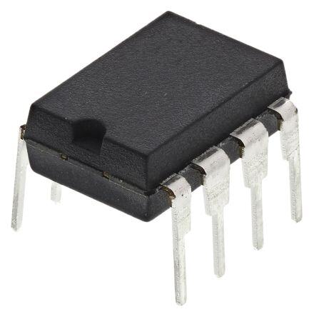
| 描述 | IC MOSFET DRVR SGL HS 9A 8-DIP门驱动器 Sgl 9-A H-S L-S MOSFET Driver |
| 产品分类 | PMIC - MOSFET,电桥驱动器 - 外部开关集成电路 - IC |
| 品牌 | Texas Instruments |
| 产品手册 | |
| 产品图片 |
|
| rohs | 符合RoHS无铅 / 符合限制有害物质指令(RoHS)规范要求 |
| 产品系列 | 电源管理 IC,门驱动器,Texas Instruments UCC37321P- |
| 数据手册 | |
| 产品型号 | UCC37321P |
| 上升时间 | 35 ns |
| 下降时间 | 20 ns |
| 产品目录页面 | |
| 产品种类 | 门驱动器 |
| 供应商器件封装 | 8-PDIP |
| 其它名称 | 296-13686-5 |
| 包装 | 管件 |
| 单位重量 | 440.400 mg |
| 商标 | Texas Instruments |
| 安装类型 | 通孔 |
| 安装风格 | Through Hole |
| 封装 | Tube |
| 封装/外壳 | 8-DIP(0.300",7.62mm) |
| 封装/箱体 | PDIP-8 |
| 工作温度 | 0°C ~ 70°C |
| 工厂包装数量 | 50 |
| 延迟时间 | 25ns |
| 最大功率耗散 | 350 mW |
| 最大工作温度 | + 70 C |
| 最小工作温度 | 0 C |
| 标准包装 | 50 |
| 激励器数量 | 1 Driver |
| 电压-电源 | 4 V ~ 15 V |
| 电流-峰值 | 9A |
| 电源电压-最大 | 15 V |
| 电源电压-最小 | 4 V |
| 电源电流 | 0.65 mA |
| 类型 | Low Side |
| 系列 | UCC37321 |
| 输入类型 | 反相 |
| 输出数 | 1 |
| 输出电流 | 9 A |
| 输出端数量 | 1 |
| 配置 | Inverting |
| 配置数 | 1 |
| 高压侧电压-最大值(自举) | - |


- 商务部:美国ITC正式对集成电路等产品启动337调查
- 曝三星4nm工艺存在良率问题 高通将骁龙8 Gen1或转产台积电
- 太阳诱电将投资9.5亿元在常州建新厂生产MLCC 预计2023年完工
- 英特尔发布欧洲新工厂建设计划 深化IDM 2.0 战略
- 台积电先进制程称霸业界 有大客户加持明年业绩稳了
- 达到5530亿美元!SIA预计今年全球半导体销售额将创下新高
- 英特尔拟将自动驾驶子公司Mobileye上市 估值或超500亿美元
- 三星加码芯片和SET,合并消费电子和移动部门,撤换高东真等 CEO
- 三星电子宣布重大人事变动 还合并消费电子和移动部门
- 海关总署:前11个月进口集成电路产品价值2.52万亿元 增长14.8%


PDF Datasheet 数据手册内容提取
Product Sample & Technical Tools & Support & Folder Buy Documents Software Community UCC27321,UCC27322 UCC37321,UCC37322 SLUS504H–SEPTEMBER2002–REVISEDJANUARY2016 UCC2732x/UCC3732x Single 9-A High-Speed Low-Side Mosfet Driver With Enable 1 Features 2 Applications • Industry-StandardPin-OutWithAdditionofEnable • SwitchModePowerSupplies 1 Function • DC-DCConverters • High-PeakCurrentDriveCapabilityof±9Aat • MotorControllers theMillerplateauregionUsingTrueDrive • Class-DSwitchingAmplifiers • EfficientConstantCurrentSourcingUsinga • LineDrivers UniqueBiPolarandCMOSOutputStage • PulseTransformerDrivers • TTL/CMOSCompatibleInputsIndependentof SupplyVoltage 3 Description • 20-nsTypicalRiseandFallTimesWith10-nF The UCC2732x/UCC3732x family of high-speed Load drivers deliver 9 A of peak drive current in an industry • TypicalPropagationDelayTimesof25nsWith standard pinout. These drivers can drive the largest InputFallingand35nsWithInputRising of MOSFETs for systems requiring extreme Miller current due to high dV/dt transitions. This eliminates • 4-Vto15-VSupplyVoltage additional external circuits and can replace multiple • AvailableinThermallyEnhancedMSOP components to reduce space, design complexity, and PowerPAD™PackageWith4.7°C/Wθjc assembly cost. Two standard logic options are • RatedFrom –40°Cto+105°C offered, inverting (UCC37321) and noninverting (UCC37322). • Pb-FreeFinish(CUNIPDAU)on8-pinSOICand PDIPPackages DeviceInformation(1) PART PACKAGE BODYSIZE(NOM) NUMBER MSOP-PowerPAD(8) 3.00mm×3.00mm UCC2732x SOIC(8) 3.91mm×4.90mm UCC3732x PDIP(8) 6.35mm×9.81mm (1) For all available packages, see the orderable addendum at theendofthedatasheet. BlockDiagram VDD 1 8 VDD INVERTING 7 OUT VDD NON-- IN 2 INVERTING 6 OUT R ENBL 100kΩ ENBL 3 AGND 4 5 PGND 1 An IMPORTANT NOTICE at the end of this data sheet addresses availability, warranty, changes, use in safety-critical applications, intellectualpropertymattersandotherimportantdisclaimers.PRODUCTIONDATA.
UCC27321,UCC27322 UCC37321,UCC37322 SLUS504H–SEPTEMBER2002–REVISEDJANUARY2016 www.ti.com Table of Contents 1 Features.................................................................. 1 8.4 DeviceFunctionalModes........................................14 2 Applications........................................................... 1 9 ApplicationandImplementation........................ 15 3 Description............................................................. 1 9.1 ApplicationInformation............................................15 4 RevisionHistory..................................................... 2 9.2 TypicalApplication .................................................15 5 Description(continued)......................................... 3 10 PowerSupplyRecommendations..................... 19 6 PinConfigurationandFunctions......................... 3 11 Layout................................................................... 19 11.1 LayoutGuidelines.................................................19 7 Specifications......................................................... 4 11.2 LayoutExample....................................................20 7.1 AbsoluteMaximumRatings......................................4 11.3 ThermalInformation..............................................20 7.2 ESDRatings..............................................................4 12 DeviceandDocumentationSupport................. 21 7.3 RecommendedOperatingConditions.......................4 7.4 ThermalInformation..................................................4 12.1 DeviceSupport......................................................21 7.5 ElectricalCharacteristics...........................................5 12.2 DocumentationSupport........................................21 7.6 SwitchingCharacteristics..........................................6 12.3 RelatedLinks........................................................21 7.7 PowerDissipationRatings........................................6 12.4 CommunityResources..........................................21 7.8 TypicalCharacteristics..............................................8 12.5 Trademarks...........................................................21 12.6 ElectrostaticDischargeCaution............................22 8 DetailedDescription............................................ 12 12.7 Glossary................................................................22 8.1 Overview.................................................................12 13 Mechanical,Packaging,andOrderable 8.2 FunctionalBlockDiagram.......................................12 Information........................................................... 22 8.3 FeatureDescription.................................................12 4 Revision History NOTE:Pagenumbersforpreviousrevisionsmaydifferfrompagenumbersinthecurrentversion. ChangesfromRevisionG(May2013)toRevisionH Page • AddedESDRatingstable,FeatureDescriptionsection,DeviceFunctionalModes,ApplicationandImplementation section,PowerSupplyRecommendationssection,Layoutsection,DeviceandDocumentationSupportsection,and Mechanical,Packaging,andOrderableInformationsection.................................................................................................. 1 ChangesfromRevisionF(March2012)toRevisionG Page • UpdatedAGNDpindescription. ............................................................................................................................................ 3 • Changedminimumvalueforinputvoltagefrom–5to–0.3VintheAbsoluteMaximumRatingstable................................ 4 • AddedC =10nFtoFallTimevsSupplyVoltagegraph................................................................................................. 8 LOAD • ChangedChangedx-axisvaluesfrom1,10,100to0.1,1,10inRiseTimevsLoadCapacitancegraph........................... 8 • ChangedChangedx-axisvaluesfrom1,10,100to0.1,1,10inFallTimevsOutputCapacitancegraph.......................... 8 2 SubmitDocumentationFeedback Copyright©2002–2016,TexasInstrumentsIncorporated
UCC27321,UCC27322 UCC37321,UCC37322 www.ti.com SLUS504H–SEPTEMBER2002–REVISEDJANUARY2016 5 Description (continued) Using a design that inherently minimizes shoot-through current, the outputs of these can provide high gate drive current where it is most needed at theMiller plateau region during the MOSFET switching transition. A unique hybridoutputstageparallelingbipolarandMOSFETtransistors(TrueDrive)allowsefficientcurrentdeliveryatlow supply voltages. With this drive architecture, UCC3732x can be used in industry standard 6-A, 9-A and many 12- A driver applications. Latch up and ESD protection circuitries are also included. Finally, the UCC3732x provides anenable(ENBL)functiontohavebettercontroloftheoperationofthedriverapplications.ENBLisimplemented on pin 3, which was previously left unused in the industry standard pinout. It is internally pulled up to V for DD activehighlogicandcanbeleftopenforstandardoperation. In addition to the 8-pin SOIC (D) and 8-pin PDIP (P) package offerings, the UCC3732x also comes in the thermally enhanced but tiny 8-pin MSOP PowerPAD™ (DGN) package. The PowerPAD package drastically lowersthethermalresistancetoextendthetemperatureoperationrangeandimprovethelong-termreliability. 6 Pin Configuration and Functions P,D,andDGNPackages 8-PinPDIP,SOIC,andMSOPWithPowerPAD TopView VDD 1 8 VDD IN 2 7 OUT ENBL 3 6 OUT AGND 4 5 PGND PinFunctions PIN I/O DESCRIPTION NAME NO. TheAGNDandthePGNDmustbeconnectedbyasinglethicktracedirectlyunderthe device.TheremustbealowESR,lowESLcapacitorof0.1µFbetweenVDD(pin8)and PGNDandaseparate0.1-µFcapacitorbetweenVDD(pin1)andAGND.Thepower AGND 4 — MOSFETsmustbelocatedonthePGNDsideofthedevicewhilethecontrolcircuitmustbe ontheAGNDsideofthedevice.ThecontrolcircuitgroundmustbecommonwiththeAGND whilethePGNDmustbecommonwiththesourceofthepowerFETs. Enableinputforthedriverwithlogiccompatiblethresholdandhysteresis.Thedriveroutput canbeenabledanddisabledwiththispin.ItisinternallypulleduptoV with100-kΩ ENBL 3 I DD resistorforactivehighoperation.Whenthedeviceisdisabled,theoutputstateis,low regardlessoftheinputstate. IN 2 I Inputsignalofthedriverwhichhaslogiccompatiblethresholdandhysteresis. Driveroutputsthatmustbeconnectedtogetherexternally.Theoutputstageiscapableof OUT 6,7 O providing9-ApeakdrivecurrenttothegateofapowerMOSFET. Commongroundforoutputstage.Thisgroundmustbeconnectedverycloselytothesource PGND 5 — ofthepowerMOSFETwhichthedriverisdriving.Groundsareseparatedtominimizeringing affectsduetooutputswitchingdi/dtwhichcanaffecttheinputthreshold. Supplyvoltageandthepowerinputconnectionsforthisdevice.Twopinsmustbeconnected VDD 1,8 I togetherexternally. Copyright©2002–2016,TexasInstrumentsIncorporated SubmitDocumentationFeedback 3
UCC27321,UCC27322 UCC37321,UCC37322 SLUS504H–SEPTEMBER2002–REVISEDJANUARY2016 www.ti.com 7 Specifications 7.1 Absolute Maximum Ratings overoperatingfree-airtemperaturerange(unlessotherwisenoted) (1)(2) MIN MAX UNIT Supplyvoltage,V –0.3 16 V DD Outputcurrent(OUT)DC,I 0.6 A OUT_DC Inputvoltage(IN),V –0.3 6VorV +0.3(3) V IN DD Enablevoltage(ENBL) –0.3 6VorV +0.3(3) V DD Dpackage 650 mW PowerdissipationatT =25°C DGNpackage 3 W A Ppackage 350 mW Leadtemperature(soldering,10s) 300 °C Junctionoperatingtemperature,T –55 150 °C J Storagetemperature,T –65 150 °C stg (1) StressesbeyondthoselistedunderAbsoluteMaximumRatingsmaycausepermanentdamagetothedevice.Thesearestressratings only,whichdonotimplyfunctionaloperationofthedeviceattheseoranyotherconditionsbeyondthoseindicatedunderRecommended OperatingConditionsRecommendedOperatingConditions.Exposuretoabsolute-maximum-ratedconditionsforextendedperiodsmay affectdevicereliability. (2) AllvoltagesarewithrespecttoGND.Currentsarepositiveinto,negativeoutofthespecifiedterminal. (3) Whicheverislarger 7.2 ESD Ratings VALUE UNIT Human-bodymodel(HBM),perANSI/ESDA/JEDECJS-001(1) ±2500 V(ESD) Electrostaticdischarge Charged-devicemodel(CDM),perJEDECspecificationJESD22- V C101(2) ±1500 (1) JEDECdocumentJEP155statesthat500-VHBMallowssafemanufacturingwithastandardESDcontrolprocess. (2) JEDECdocumentJEP157statesthat250-VCDMallowssafemanufacturingwithastandardESDcontrolprocess. 7.3 Recommended Operating Conditions overoperatingfree-airtemperaturerange(unlessotherwisenoted) MIN NOM MAX UNIT Supplyvoltage,VDD 4.5 15 V 7.4 Thermal Information UCC27322 UCC27321 THERMALMETRIC(1) D(SOIC) P(PDIP) DGN(MSOP- UNIT PowerPAD) 8PINS 8PINS 8PINS R Junction-to-ambientthermalresistance 56.6 55.9 56.7 °C/W θJA R Junction-to-case(top)thermalresistance 52.8 45.3 52.9 °C/W θJC(top) R Junction-to-boardthermalresistance 32.6 32.6 32.7 °C/W θJB ψ Junction-to-topcharacterizationparameter 1.8 23.0 1.8 °C/W JT ψ Junction-to-boardcharacterizationparameter 32.3 32.5 32.4 °C/W JB R Junction-to-case(bottom)thermalresistance 5.9 — 5.9 °C/W θJC(bot) (1) Formoreinformationabouttraditionalandnewthermalmetrics,seetheSemiconductorandICPackageThermalMetricsapplication report,SPRA953. 4 SubmitDocumentationFeedback Copyright©2002–2016,TexasInstrumentsIncorporated
UCC27321,UCC27322 UCC37321,UCC37322 www.ti.com SLUS504H–SEPTEMBER2002–REVISEDJANUARY2016 7.5 Electrical Characteristics V =4.5Vto15V,T =–40°Cto+105°CforUCC2732x,T =0°Cto70°CforUCC3732x,T =T,unlessotherwisenoted. DD A A A J PARAMETER TESTCONDITIONS MIN TYP MAX UNIT INPUT(IN) V ,logic1inputthreshold 2 V IN_H V ,logic0inputthreshold 1 V IN_L Inputcurrent 0V≤V ≤V –10 0 10 µA IN DD OUTPUT(OUT) Peakoutputcurrent(1)(2) V =14V, 9 A DD V ,outputhighlevel V =V –V ,I =–10mA 150 300 mV OH OH DD OUT OUT V ,outputlowlevel I =10mA 11 25 mV OL OUT Outputresistancehigh(3) I =–10mA,V =14V 15 25 Ω OUT DD Outputresistancelow(3) I =10mA,V =14V 1.1 2.2 Ω OUT DD Latch--upprotection(1) 500 mA OVERALL IN=LOW,EN=LOW,V =15V 150 225 DD UCC37321 IN=HIGH,EN=LOW,VDD=15V 440 650 UCC27321 IN=LOW,EN=HIGH,V =15V 370 550 DD IN=HIGH,EN=HIGH,V =15V 370 550 DD I ,staticoperatingcurrent µA DD IN=LOW,EN=LOW,V =15V 150 225 DD UCC37322 IN=HIGH,EN=LOW,VDD=15V 450 650 UCC27322 IN=LOW,EN=HIGH,V =15V 75 125 DD IN=HIGH,EN=HIGH,V =15V 675 1000 DD ENABLE(ENBL) V ,high-levelinputvoltage LOWtoHIGHtransition 1.7 2.2 2.7 V IN_H V ,low-levelinputvoltage HIGHtoLOWtransition 1.1 1.6 2 IN_L V Hysteresis 0.25 0.55 0.90 R ,enableimpedance V =14V,ENBL=GND 75 100 135 kΩ ENBL DD (1) Ensuredbydesign.Nottestedinproduction. (2) ThepullupandpulldowncircuitsofthedriverarebipolarandMOSFETtransistorsinparallel.Thepeakoutputcurrentratingisthe combinedcurrentfromthebipolarandMOSFETtransistors. (3) ThepullupandpulldowncircuitsofthedriverarebipolarandMOSFETtransistorsinparallel.TheoutputresistanceistheR ofthe DS(ON) MOSFETtransistorwhenthevoltageonthedriveroutputislessthanthesaturationvoltageofthebipolartransistor. Copyright©2002–2016,TexasInstrumentsIncorporated SubmitDocumentationFeedback 5
UCC27321,UCC27322 UCC37321,UCC37322 SLUS504H–SEPTEMBER2002–REVISEDJANUARY2016 www.ti.com 7.6 Switching Characteristics overoperatingfree-airtemperaturerange(unlessotherwisenoted) PARAMETER TESTCONDITIONS MIN TYP MAX UNIT ENABLE(ENBL) t ,propagationdelaytime(1) C =10nF 60 90 ns D3 LOAD t ,propagationdelaytime(1) C =10nF 60 90 ns D4 LOAD SWITCHINGTIME(2) t ,risetime(OUT) C =10nF 20 70 ns R LOAD t ,falltime(OUT) C =10nF 20 30 ns F LOAD t ,propagationdelay,INrising(INtoOUT) C =10nF 25 70 ns D1 LOAD t ,propagationdelay,INfalling(INtoOUT) C =10nF 35 70 ns D2 LOAD (1) SeeFigure2. (2) SeeFigure1forswitchingwaveforms. 7.7 Power Dissipation Ratings PowerRating DeratingFactor PACKAGE SUFFIX θjc(°C/W) θja(°C/W) (mW) Above T =70°C(1) 70°C(mW/°C)(1) A SOIC-8 D 42 84to160(2) 344to655(2) 6.25to11.9(2) PDIP-8 P 49 110 500 9 MSOPPowerPAD-8 DGN 4.7 50to59 1370 17.1 (1) 125°Coperatingjunctiontemperatureisusedforpowerratingcalculations (2) Therangeofvaluesindicatestheeffectoftheprinted-circuit-board.Thesevaluesareintendedtogivethesystemdesigneranindication ofthebestandworstcaseconditions.Ingeneral,thesystemdesignershouldattempttouselargertracesontheprinted-circuit-board wherepossibletospreadtheheatawayformthedevicemoreeffectively.Foradditionalinformationondevicetemperature management,seethePackagingInformationsectionofthePowerSupplyControlProductsDataBook,(SLUD003). (a) (b) 5V IN VTH VTH IN VTH VTH 0V tD1 tD2 tD1 tD2 tF VDD 80% 80% 80% 80% OUT tR OUT tR tF 20% 20% 0V The20%and80%thresholdsdepictthedynamicsoftheBiPolaroutputdevicesthatdominatethepowerMOSFET transitionthroughtheMillerregionsofoperation. Figure1. SwitchingWaveformsfor(a)InvertingInputto(b)OutputTimes 6 SubmitDocumentationFeedback Copyright©2002–2016,TexasInstrumentsIncorporated
UCC27321,UCC27322 UCC37321,UCC37322 www.ti.com SLUS504H–SEPTEMBER2002–REVISEDJANUARY2016 5V ENBL VIN_H VIN_L 0V tD3 tD4 VDD 80% 80% OUT tR tF 20% 0V The20%and80%thresholdsdepictthedynamicsoftheBiPolaroutputdevicesthatdominatethepowerMOSFET transitionthroughtheMillerregionsofoperation. Figure2. SwitchingWaveformforEnabletoOutput Copyright©2002–2016,TexasInstrumentsIncorporated SubmitDocumentationFeedback 7
UCC27321,UCC27322 UCC37321,UCC37322 SLUS504H–SEPTEMBER2002–REVISEDJANUARY2016 www.ti.com 7.8 Typical Characteristics 700 700 600 600 μA ENINBL= =5V 0V μA ENBL= 0V – 500 – 500 IN= 5V I–InputCurrentIdleDD 423000000 ENINBL= =5 VVDD ENINBL= =0V 0V I–InputCurrentIdleDD 423000000 ENINBL= =0V 0V ENBL= VDD, IENN I=NB 0L=V =5 VVDD 100 100 0 ENBL= VDD, IN = 0V 0 0 2 4 6 8 10 12 14 16 0 2 4 6 8 10 12 14 16 VDD–Supply Voltage–V VDD–Supply Voltage–V Figure3.InputCurrentIdlevsSupplyVoltage(UCCx7321) Figure4.InputCurrentIdlevsSupplyVoltage(UCCx7322) 800 800 700 700 ENBL= HIIGH IN=HIIGH A–CurrentIdleμ 645000000 EINN=B LHI= LO EINN=B LHI= HI EINN=B LLO= HI CurrAentIdle–μ 645000000 EINN=B HLIIG= HLOW ut ut I–InpDD 230000 EINN=B LLO= LO I–InpDD230000 EINN=B LLO=W LOW EINN=B LLO=W HIIGH 100 100 0 0 --50 --25 0 25 50 75 100 125 --50 --25 0 25 50 100 75 125 TJ–Temperature–°C TJ–Temperature–°C Figure5.InputCurrentIdlevsTemperature(UCCx7321) Figure6.InputCurrentIdlevsTemperature(UCCx7322) 70 70 CLOAD=10nF CLOAD= 10 nF 60 60 50 tA=–40°C 50 s s n –n 40 e– 40 Rise Time 30 tA=105°C tA=25°C –Fall Tim 30 tA=105°C tA=25°C t–R 20 tR 20 10 tA=0°C 10 tA=0°C tA=–40°C 0 0 4 6 8 10 12 14 16 4 6 8 10 12 14 16 VDD–SupplyVoltage–V VDD-- SupplyVoltage--V Figure7.RiseTimevsSupplyVoltage Figure8.FallTimevsSupplyVoltage 8 SubmitDocumentationFeedback Copyright©2002–2016,TexasInstrumentsIncorporated
UCC27321,UCC27322 UCC37321,UCC37322 www.ti.com SLUS504H–SEPTEMBER2002–REVISEDJANUARY2016 Typical Characteristics (continued) 40 200 VDD=5V VDD=5V 160 30 VDD=10V ns VDD=10V s VDD=15V me– VDD=15V e–n 120 t–Rise TiR 20 t–Fall TimR 80 10 40 0 0 0.1 1 10 0.1 1 10 CLOAD–- LoadCapacitance–nF CLOAD– LoadCapacitance–nF Figure9.RiseTimevsLoadCapacitance Figure10.FallTimevsOutputCapacitance 70 70 CLOAD=10nF CLOAD=10nF 60 60 tA=105°C tA=105°C ns 50 50 tA=25°C e-- tA=25°C ns DelayTim 40 ayTime-- 40 -– 30 Del 30 tD1 20 t–D2 20 tA=0°C tA=–40°C tA=–40°C 10 tA=0°C 10 0 0 4 6 8 10 12 14 16 4 6 8 10 12 14 16 VDD–SupplyVoltage–V VDD– SupplyVoltage–V Figure11.t DelayTimevsSupplyVoltage Figure12.t DelayTimevsSupplyVoltage D1 D2 70 70 VDD=5V 60 60 -–ns 50 VDD=5V VDD=10V e–ns 50 Time 40 yTim 40 t–DelayD1 3200 VDD=15V t–DelaD2 3200 VDD=15V VDD=10V 10 10 0 0 1 10 100 1 10 100 CLOAD– LoadCapacitance–nF CLOAD–LoadCapacitance–nF Figure13.tD1DelayTimevsLoadCapacitance Figure14.tD2DelayTimevsLoadCapacitance Copyright©2002–2016,TexasInstrumentsIncorporated SubmitDocumentationFeedback 9
UCC27321,UCC27322 UCC37321,UCC37322 SLUS504H–SEPTEMBER2002–REVISEDJANUARY2016 www.ti.com Typical Characteristics (continued) 50 2.0 VDD=15V 45 tD2 CLTOAAD==251°0CnF 1.9 VDD=15V 40 V tRISE – 1.8 PropagationTime--ns 3231205550 nputThreshold Voltage 111...567 VDD=10V 10 tD1 tFALL V–ION 1.4 VDD=4.5 V 1.3 5 0 1.2 0 5 10 15 --50 --25 0 25 50 75 100 125 VIN(peak)– PeakInput Voltage–V TJ–Temperature–°C Figure15.PropagationTimesvsPeakInputVoltage Figure16.InputThresholdvsTemperature 3.0 150 140 ENBL--ON 2.5 V 130 esis– Ωe– 120 Enablethresholdandhyster 112...050 ENBL--OFF R–EnableResistancENBL 111078900000 0.5 ENBL--HYSTERESIS 60 0 50 --50 --25 0 25 50 75 100 125 --50 --25 0 25 50 75 100 125 TJ– Temperature–°C TJ–Temperature– °C Figure17.EnableThresholdandHysteresisvsTemperature Figure18.EnableResistancevsTemperature IN= GND IN= GND ENBL= VDD ENBL= VDD V V – – –Input Voltage1 V/div –InputVoltage1V/div VDD VDD VDD OUT OUT 0V 0V VDD 10nF Between Output and GND 10nF Between Output and GND 50μs/div 50μs/div Figure19.OutputBehaviorvsVDD(UCC37321) Figure20.OutputBehaviorvsVDD(UCC37321) 10 SubmitDocumentationFeedback Copyright©2002–2016,TexasInstrumentsIncorporated
UCC27321,UCC27322 UCC37321,UCC37322 www.ti.com SLUS504H–SEPTEMBER2002–REVISEDJANUARY2016 Typical Characteristics (continued) ENINBL= V= DVDDD ENINBL= V= DVDDD V – ge V SupplyVolta1V/div VDD plyVoltage–V/div VDD – up1 D S VD OUT – OUT D D V 0V 0V 10nF Between Output and GND 10nF Between Output and GND 50μs/div 50μs/div Figure21.OutputBehaviorvsVDD(Inverting) Figure22.OutputBehaviorvsVDD(Inverting) IN= GND IN= GND ENBL= VDD ENBL= VDD V V – – –SupplyVoltage1V/div VDD OUT –SupplyVoltage1V/div OUT VDD D D D D V V 0V 0V 10nF Between Output and GND 10nF Between Output and GND 50μs/div 50μs/div Figure23.OutputBehaviorvsVDD(Noninverting) Figure24.OutputBehaviorvsVDD(Noninverting) Copyright©2002–2016,TexasInstrumentsIncorporated SubmitDocumentationFeedback 11
UCC27321,UCC27322 UCC37321,UCC37322 SLUS504H–SEPTEMBER2002–REVISEDJANUARY2016 www.ti.com 8 Detailed Description 8.1 Overview The UCC37321 and UCC37322 drivers serve as an interface between low-power controllers and power MOSFETs. They can also be used as an interface between DSPs and power MOSFETs. High-frequency power supplies often require high-speed, high-current drivers such as the UCC3732x family. A leading application is the need to provide a high power buffer stage between the PWM output of the control device and the gates of the primary power MOSFET or IGBT switching devices. In other cases, the device drives the power device gates through a drive transformer. Synchronous rectification supplies must simultaneously drive multiple devices which canpresentanextremelylargeloadtothecontrolcircuitry. The inverting driver (UCC37321) is useful for generating inverted gate drive signals from controllers that have only outputs of the opposite polarity. For example, this driver can provide a gate signal for ground referenced, N-channel synchronous rectifier MOSFETs in buck derived converters. This driver can also be used for generating a gate drive signal for a P-channel MOSFET from a controller that is designed for N-channel applications. MOSFET gate drivers are generally used when it is not feasible to have the primary PWM regulator device directly drive the switching devices for one or more reasons. The PWM device may not have the brute drive capability required for the intended switching MOSFET, limiting the switching performance in the application. In other cases there may be a desire to minimize the effect of high-frequency switching noise by placing the high current driver physically close to the load. Also, newer devices that target the highest operating frequencies may not incorporate onboard gate drivers at all. Their PWM outputs are only intended to drive the high impedance input to a driver such as the UCC3732x. Finally, the control device may be under thermal stress due to power dissipation,andanexternaldrivercanhelpbymovingtheheatfromthecontrollertoanexternalpackage. 8.2 Functional Block Diagram VDD 1 8 VDD INVERTING 7 OUT VDD NON-- IN 2 INVERTING 6 OUT R ENBL 100kΩ ENBL 3 AGND 4 5 PGND 8.3 Feature Description 8.3.1 InputStage The IN threshold has a 3.3-V logic sensitivity over the full range of VDD voltages; yet, it is equally compatible with 0 V to VDD signals. The inputs of UCC3732x family of drivers are designed to withstand 500-mA reverse current without either damage to the device or logic upset. In addition, the input threshold turnoff of the UCC3732x has been slightly raised for improved noise immunity. The input stage of each driver must be driven by a signal with a short rise or fall time. This condition is satisfied in typical power supply applications, where the inputsignalsareprovidedbyaPWMcontrollerorlogicgateswithfasttransitiontimes(< 200ns).TheINinputof thedriverfunctionsasadigitalgate,anditisnotintendedforapplicationswhereaslowchanginginputvoltageis used to generate a switching output when the logic threshold of the input section is reached. While this may not beharmfultothedriver,theoutputofthedrivermayswitchrepeatedlyatahighfrequency. 12 SubmitDocumentationFeedback Copyright©2002–2016,TexasInstrumentsIncorporated
UCC27321,UCC27322 UCC37321,UCC37322 www.ti.com SLUS504H–SEPTEMBER2002–REVISEDJANUARY2016 Feature Description (continued) Users should not attempt to shape the input signals to the driver in an attempt to slow down (or delay) the signal at the output. If limiting the rise or fall times to the power device is desired, then an external resistance can be added between the output of the driver and the load device, which is generally a power MOSFET gate. The external resistor may also help remove power dissipation from the device package, as discussed in Thermal Information. 8.3.2 OutputStage The TrueDrive output stage is capable of supplying ±9-A peak current pulses; it swings to both VDD and GND and can encourage even the most stubborn MOSFETs to switch. The pullup and pulldown circuits of the driver are constructed of bipolar and MOSFET transistors in parallel. The peak output current rating is the combined current from the bipolar and MOSFET transistors. The output resistance is the R of the MOSFET transistor DS(ON) when the voltage on the driver output is less than the saturation voltage of the bipolar transistor. Each output stage also provides a very low impedance to overshoot and undershoot due to the body diode of the internal MOSFET.Thismeansthatinmanycases,external-schottky-clampdiodesarenotrequired. This unique BiPolar and MOSFET hybrid output architecture (TrueDrive) allows efficient current sourcing at low supply voltages. The UCC3732x family delivers 9 A of gate drive where it is most needed during the MOSFET switchingtransition– attheMillerplateauregion – providingimprovedefficiencygains. 8.3.3 SourceandSinkCapabilitiesduringMillerPlateau Large power MOSFETs present a significant load to the control circuitry. Proper drive is required for efficient, reliable operation. The UCC3732x drivers have been optimized to provide maximum drive to a power MOSFET during the Miller plateau region of the switching transition. This interval occurs while the drain voltage is swinging betweenthevoltagelevelsdictatedbythepowertopology,requiringthechargingordischargingofthedrain-gate capacitancewithcurrentsuppliedorremovedbythedriverdevice. Two circuits are used to test the current capabilities of the UCC3732x driver (see Reference (1)) . In each case external circuitry is added to clamp the output near 5 V while the device is sinking or sourcing current. An input pulse of 250 ns is applied at a frequency of 1 kHz in the proper polarity for the respective test. In each test there is a transient period where the current peaked up and then settled down to a steady-state value. The noted currentmeasurementsaremadeatatimeof200nsaftertheinputpulseisapplied,aftertheinitialtransient. The circuit in Figure 25 is used to verify the current sink capability when the output of the driver is clamped around 5 V, a typical value of gate-source voltage during the Miller plateau region. The UCC37321 is found to sink9AatV =15V. DD VDD UCC37321 INPUT 1 VDD VDD 8 IN OUT DSCHOTTKY 10Ω 2 7 OUT C2 C3 + VSUPPLY 3 ENBL 6 1μF 100μF 5.5V 4 AGND PGND 5 VSNS 1μF 100μF 0R.S1NΩS CER ALEL UDG--01113 Figure25. SinkCurrentTestCircuit The circuit in Figure 26 is used to test the current source capability with the output clamped to around 5 V with a stringofZenerdiodes.TheUCC37321isfoundtosource9AatV =15V. DD Copyright©2002–2016,TexasInstrumentsIncorporated SubmitDocumentationFeedback 13
UCC27321,UCC27322 UCC37321,UCC37322 SLUS504H–SEPTEMBER2002–REVISEDJANUARY2016 www.ti.com Feature Description (continued) VDD UCC37321 INPUT 1 VDD VDD 8 DSCHOTTKY IN OUT 2 7 3 ENBL OUT 6 C1μ2F C1030μF 4D.A5DVJ 4 AGND PGND 5 VSNS RSNS 1μF 100μF 0.1Ω CER ALEL UDG--01114 Figure26. SourceCurrentTestCircuit Note that the current sink capability is slightly stronger than the current source capability at lower VDD. This is due to the differences in the structure of the bipolar-MOSFET power output section, where the current source is aP-channelMOSFETandthecurrentsinkhasanN-channelMOSFET. In most it is advantageous that the turnoff capability of a driver is stronger than the turnon capability. This helps toensurethattheMOSFETisheldOFFduringcommonpowersupplytransientswhichmayturnthedeviceback ON. 8.3.4 Enable The UCC37321/2 provides an enable input for improved control of the driver operation. This input also incorporates logic compatible thresholds with hysteresis. It is internally pulled up to VDD with 100-kΩ resistor for active high operation. When ENBL is high, the device is enabled and when ENBL is low, the device is disabled. The default state of the ENBL pin is to enable the device and therefore it can be left open for standard operation. The output state when the device is disabled is low regardless of the input state. See Table 1 for the operation usingenablelogic. ENBL input is compatible with both logic signals and slow changing analog signals. It can be directly driven or a power-updelaycanbeprogrammedwithacapacitorbetweenENBLandAGND. 8.4 Device Functional Modes Table1liststhelogicofthisdevice. Table1.DeviceLogicTable ENBL IN OUT 0 0 0 INVERTING 0 1 0 UCC37321 1 0 1 1 1 0 0 0 0 NON-- 0 1 0 INVERTING UCC37322 1 0 0 1 1 1 14 SubmitDocumentationFeedback Copyright©2002–2016,TexasInstrumentsIncorporated
UCC27321,UCC27322 UCC37321,UCC37322 www.ti.com SLUS504H–SEPTEMBER2002–REVISEDJANUARY2016 9 Application and Implementation NOTE Information in the following applications sections is not part of the TI component specification, and TI does not warrant its accuracy or completeness. TI’s customers are responsible for determining suitability of components for their purposes. Customers should validateandtesttheirdesignimplementationtoconfirmsystemfunctionality. 9.1 Application Information High-current gate driver devices are required in switching power applications for a variety of reasons. To enable fast switching of power devices and reduce associated power losses, a powerful gate driver can be employed between the PWM output of controllers or signal isolation devices and the gates of the power semiconductor devices. Further, gate drivers are indispensable when sometimes it is just not feasible to have the PWM controller directly drive the gates of the switching devices. The situation may be encountered because the PWM signalfromadigitalcontrollerorsignalisolationdeviceisoftena3.3-Vor5-Vlogicsignalwhichisnotcapableof effectivelyturningonapowerswitch.Alevel-shiftingcircuitryisneededtoboostthelogic-levelsignaltothegate- drive voltage to fully turn on the power device and minimize conduction losses. Traditional buffer drive circuits based on NPN/PNP bipolar, (or P- N- channel MOSFET), transistors in totem-pole arrangement, being emitter follower configurations, prove inadequate for this because they lack level-shifting capability and low-drive voltage protection. Gate drivers effectively combine both the level-shifting and buffer drive functions. Gate drivers may also minimize the effect of switching noise by locating the high-current driver physically close to the power switch, drive gate-driver transformers and control floating power device gates, reducing power dissipation and thermalstressincontrollersbyabsorbinggate-chargepowerlosses. In summary gate drivers are extremely important components in switching power combining benefits of high- performance,low-cost,lowcomponentcount,board-spacereduction,andsimplifiedsystemdesign. 9.2 Typical Application 8 VDD OUT 6 Q1 C2 1 VDD OUT 7 R4 UCC27322D 2 IN AGND 4 INPUT 3 ENBL PGND 5 ENABLE Figure27. TypicalApplicationDiagramofUCC27322andUCC37322 9.2.1 DesignRequirements When selecting the proper gate driver device for an end application, some design considerations must be evaluated first to make the most appropriate selection. The following design parameters should be used when selecting the proper gate driver device for an end application: input-to-output configuration, the input threshold type, bias supply voltage levels, peak source and sink currents, availability of independent enable and disable functions, propagation delay, power dissipation, and package type. See the example design parameters and requirementsinTable2. Copyright©2002–2016,TexasInstrumentsIncorporated SubmitDocumentationFeedback 15
UCC27321,UCC27322 UCC37321,UCC37322 SLUS504H–SEPTEMBER2002–REVISEDJANUARY2016 www.ti.com Table2.DesignParameters DESIGNPARAMETER EXAMPLEVALUE Input-to-outputconfiguration Noninverting Inputthresholdtype CMOS Biassupplyvoltagelevels 12V dVDS/dt(1) 20V/ns Enablefunction Yes Propagationdelay <50ns Powerdissipation <0.45W Packagetype SOIC(8) (1) dVDS/dtisatypicalrequirementforagivendesign.Thisvaluecan beusedtofindthepeaksource/sinkcurrentsneededasshownin PeakSourceandSinkCurrents. 9.2.2 DetailedDesignProcedure 9.2.2.1 Input-to-OutputConfiguration The design should specify which type of input-to-out configuration should be used. If turning on the power MOSFET or IGBT when the input signal is in high state is preferred, then a device capable of the noninverting configuration must be selected. If turning off the power MOSFET or IGBT when the input signal is in high state is preferred, then a device capable of the inverting configuration must be chosen. Based on this noninverting requirementofthisapplication,theproperdeviceoutoftheUCC27322orUCC37322shouldbeselected. 9.2.2.2 InputThresholdType The type of input voltage threshold determines the type of controller that can be used with the gate driver device. The UCC2732x and UCC3732x devices feature a TTL and CMOS-compatible input threshold logic, with wide hysteresis. The threshold voltage levels are low voltage and independent of the V supply voltage, which allows DD compatibility with both logic-level input signals from microcontrollers as well as higher-voltage input signals from analog controllers. See Electrical Characteristics for the actual input threshold voltage levels and hysteresis specificationsfortheUCC2732xandUCC3732xdevices. 9.2.2.3 VDDBiasSupplyVoltage The bias supply voltage to be applied to the V pins of the device must never exceed the values listed in DD Recommended Operating Conditions. However, different power switches require different voltage levels to be applied at the gate. With a wide operating range from 4.5 V to 15 V, the UCC2732x and UCC3732x can be used to drive a variety of power switches, such as Si MOSFETs (for example, Vgs = 4.5 V, 10 V, 12 V), IGBTs (V =15 V), and wide-bandgap power semiconductors (such as GaN, certain types of which allow no higher than GE 6Vtobeappliedtothegateterminals). 9.2.2.4 PeakSourceandSinkCurrents Generally, the switching speed of the power switch during turnon and turnoff must be as fast as possible to minimize switching power losses. The gate driver device must be able to provide the required peak current for achievingthetargetedswitchingspeedsforthetargetedpowerMOSFET. Using the example of a power MOSFET, the system requirement for the switching speed is typically described in terms of the slew rate of the drain-to-source voltage of the power MOSFET (such as dvDS/dt). For example, the system requirement might state that a SPP20N60C3 power MOSFET must be turned on with a Dvds/dt of 20 V/ns or higher under a DC bus voltage of 400 V in a continuous-conduction-mode (CCM) boost PFC-converter application. This type of application is an inductive hard-switching application and reducing switching power loss is critical. This requirement means that the entire drain-to-source voltage swing during power MOSFET turnon event (from 400 V in the OFF state to V in ON state) must be completed in approximately 20 ns or less. DS(on) When the drain-to-source voltage swing occurs, the Miller charge of the power MOSFET (Q parameter in gd SPP20N60C3 power MOSFET data sheet is 33 nC typically) is supplied by the peak current of gate driver. According to power MOSFET inductive switching mechanism, the gate-to-source voltage of the power MOSFET at this time is the Miller plateau voltage, which is typically a few volts higher than the threshold voltage of the powerMOSFET,V ). GS(th) 16 SubmitDocumentationFeedback Copyright©2002–2016,TexasInstrumentsIncorporated
UCC27321,UCC27322 UCC37321,UCC37322 www.ti.com SLUS504H–SEPTEMBER2002–REVISEDJANUARY2016 To achieve the targeted Dvds/dt, the gate driver must be capable of providing the Q charge in 20 ns or less. In gd other words, a peak current of 1.65 A (= 33 nC) / 20 ns) or higher must be provided by the gate driver. The UCC2732x and UCC3732x devices can provide 9-A peak sourcing/sinking current which clearly exceeds the design requirement and has the capability to meet the switching speed needed. This 9-A peak sourcing/sinking currentprovidesanextramarginagainstpart-to-partvariationsintheQ parameterofthepowerMOSFETalong gd with additional flexibility to insert external gate resistors and fine tune the switching speed for efficiency versus EMI optimizations. However, in practical designs the parasitic trace in the gate driver circuit of the PCB will have a definitive role to play on the power MOSFET switching speed. The effort of this trace inductance is to limit the di/dtoftheoutputcurrentpulseofthegatedriver.Toillustratethiseffect,consideroutputcurrentpulsewaveform from the gate driver to be approximated to a triangular profile, where the area under the triangle (0.5 × IPEAK × time) would equal the total gate charge of the power MOSFET (Q parameter in SPP20N60C3 power MOSFET g data sheet= 87 nC typically). If the parasitic trace inductance limits the di/dt then a situation may occur in which the full peak current capability of the gate driver is not fully achieved in the time required to deliver the Q g required for the power MOSFET switching. In other words, the time parameter in the equation would dominate and the IPEAK value of the current pulse would be much less than the true peak current capability of the device, while the required Q is still delivered. Because of this, the desired switching speed may not be realized, even g when theoretical calculations indicate the gate driver can achieve the targeted witching speed. Thus, placing the gatedriverdeviceveryclosetothepowerMOSFETanddesigningatightgatedrive-loopwithminimalPCBtrace inductanceisimportanttorealizethefullpeak-currentcapabilityofthegatedriver. 9.2.2.5 EnableandDisableFunction Certain applications demand independent control of the output state of the driver without involving the input signal. A pin which offers enable and disable functions achieves the requirements. For these applications, the UCC2732xandUCC3732xaresuitableastheyfeatureaninputpinandanEnablepin. 9.2.2.6 PropagationDelay The acceptable propagation delay from the gate driver is dependent on the switching frequency at which it is used and the acceptable level of pulse distortion to the system. The UCC2732x and UCC3732x devices feature 25-ns turnon propagation delay and 35-ns turnoff propagation delay (typical), which ensure very little distortion and allow operation at higher frequencies. See Electrical Characteristics for the propagation and Switching CharacteristicsoftheUCC2732xandUCC3732xdevices. 9.2.2.7 PowerDissipation The UCC3732x family of drivers are capable of delivering 9-A of current to a MOSFET gate for a period of several hundred nanoseconds. High peak current is required to turn an N-channel device ON quickly. Then, to turn the device OFF, the driver is required to sink a similar amount of current to ground. This repeats at the operating frequency of the power device. An N-channel MOSFET is used in this discussion because it is the mostcommontypeofswitchingdeviceusedinhigh-frequencypowerconversionequipment. References (1) and (2) contain detailed discussions of the drive current required to drive a power MOSFET and other capacitive-input switching devices. Much information is provided in tabular form to give a range of the current required for various devices at various frequencies. The information pertinent to calculating gate drive currentrequirementswillbesummarizedhere;theoriginaldocumentisavailablefromtheTIwebsite. When a driver device is tested with a discrete, capacitive load it is a fairly simple matter to calculate the power that is required from the bias supply. The energy that must be transferred from the bias supply to charge the capacitorisgivenbyEquation1. 1 E= CV2 2 where • Cistheloadcapacitor • Visthebiasvoltagefeedingthedriver (1) Copyright©2002–2016,TexasInstrumentsIncorporated SubmitDocumentationFeedback 17
UCC27321,UCC27322 UCC37321,UCC37322 SLUS504H–SEPTEMBER2002–REVISEDJANUARY2016 www.ti.com There is an equal amount of energy transferred to ground when the capacitor is discharged. This leads to a powerlossgivenbyEquation2. 1 P=2 ´ CV2f 2 where • fistheswitchingfrequency (2) This power is dissipated in the resistive elements of the circuit. Thus, with no external resistor between the driver and gate, this power is dissipated inside the driver. Half of the total power is dissipated when the capacitor is charged, and the other half is dissipated when the capacitor is discharged. An example using the conditions of thepreviousgate-drivewaveformshouldhelpclarifythis. WithV =12V,C =10nF,andf=300kHz,thepowerlosscanbecalculatedasshowninEquation4. DD LOAD P=10nF×(12)2×(300kHz)=0.432W (3) Witha12-Vsupply,thiswouldequate,asshowninEquation4,toacurrentof: P 0.432W I= = =0.036A V 12V (4) The switching load presented by a power MOSFETcan be converted to an equivalent capacitance by examining the gate charge required to switch the device. This gate charge includes the effects of the input capacitance plus the added charge needed to swing the drain of the device between the ON and OFF states. Most manufacturers provide specifications that provide the typical and maximum gate charge, in nC, to switch the device under specified conditions. Using the gate charge Qg, one can determine the power that must be dissipated when chargingacapacitor.ThisisdonebyusingtheequivalenceQg=CeffVtoprovideEquation5 forpower. P=C×V2×f=Qg×V×f (5) Equation 5 allows a power designer to calculate the bias power required to drive a specific MOSFET gate at a specificbiasvoltage. 9.2.3 ApplicationCurves IN= VDD IN= VDD ENBL= VDD ENBL= VDD V V – – e e g g a a utVoltV/div utVoltV/div np1 np1 I I – – D D VD VD VDD VDD OUT OUT 0V 0V 10nF Between Output and GND 10nF Between Output and GND 50μs/div 50μs/div Figure28.OutputBehaviorvsVDD(UCC37322) Figure29.OutputBehaviorvsVDD(UCC37322) 18 SubmitDocumentationFeedback Copyright©2002–2016,TexasInstrumentsIncorporated
UCC27321,UCC27322 UCC37321,UCC37322 www.ti.com SLUS504H–SEPTEMBER2002–REVISEDJANUARY2016 10 Power Supply Recommendations Although quiescent VDD current is very low, total supply current is higher, depending on OUTA and OUTB current and the operating frequency. Total VDD current is the sum of quiescent VDD current and the average OUT current. Knowing the operating frequency and the MOSFET gate charge (Qg), average OUT current can be calculatedusingEquation6. I =Qg×f OUT where • fisfrequency (6) For the best high-speed circuit performance, TI recommends two V bypass capacitors to prevent noise DD problems. TI also highly recommends using surface mount components. A 0.1-µF ceramic capacitor must be placed closest to the VDD to ground connection. In addition, a larger capacitor (such as 1 µF) with relatively low ESR should be connected in parallel to help deliver the high current peaks to the load. The parallel combination ofcapacitorspresentsalowimpedancecharacteristicfortheexpectedcurrentlevelsinthedriverapplication. 11 Layout 11.1 Layout Guidelines It can be a significant challenge to avoid the overshoot, undershoot, and ringing issues that can arise from circuit layout. The low impedance of these drivers and their high di/dt can induce ringing between parasitic inductances andcapacitancesinthecircuit.Utmostcaremustbeusedinthecircuitlayout. In general, position the driver physically as close to its load as possible. Place a 1-µF bypass capacitor as close to the output side of the driver as possible, connecting it to pins 1 and 8. Connect a single trace between the two VDD pins (pin 1 and pin 8); connect a single trace between PGND and AGND (pin 5 and pin 4). If a ground plane is used, it may be connected to AGND; do not extend the plane beneath the output side of the package (pins 5 – 8). Connect the load to both OUT pins (pins 7 and 6) with a single trace on the adjacent layer to the component layer; route the return current path for the output on the component side, directly over the output path. Extreme conditions may require decoupling the input power and ground connections from the output power and ground connections. The UCCx732x has a feature that allows the user to take these extreme measures, if necessary. There is a small amount of internal impedance of about 15 Ω between the AGND and PGND pins; there is also a small amount of impedance (approximately 30 Ω) between the two VDD pins. To take advantage of this feature, connect a 1-µF bypass capacitor between VDD and PGND (pins 5 and 8) and connect a 0.1-µF bypass capacitor between VDD and AGND (pins 1 and 4). Further decoupling can be achieved by connecting betweenthetwoVDDpinswithajumperthatpassesthrougha40-MHzferritebeadandconnectbiaspoweronly to pin 8. Even more decoupling can be achieved by connecting between AGND and PGND with a pair of anti- paralleldiodes(anodeconnectedtocathodeandcathodeconnectedtoanode). Copyright©2002–2016,TexasInstrumentsIncorporated SubmitDocumentationFeedback 19
UCC27321,UCC27322 UCC37321,UCC37322 SLUS504H–SEPTEMBER2002–REVISEDJANUARY2016 www.ti.com 11.2 Layout Example Figure30. LayoutRecommendation 11.3 Thermal Information The useful range of a driver is greatly affected by the drive power requirements of the load and the thermal characteristics of the device package. For a power driver to be useful over a particular temperature range the package must allow for the efficient removal of the heat produced while keeping the junction temperature within rated limits. The UCC3732x family of drivers is available in three different packages to cover a range of applicationrequirements. As shown in the power dissipation rating table, the 8-pin SOIC (D) and 8-pin PDIP (P) packages each have a power rating of around 0.5 W with T = 70°C. This limit is imposed in conjunction with the power derating factor A also given in the table. The power dissipation in our earlier example is 0.432 W with a 10-nF load, 12 VDD, switched at 300 kHz. Thus, only one load of this size could be driven using the D or P package. The difficulties withheatremovallimitthedriveavailableintheDorPpackages. The 8-pin MSOP PowerPAD (DGN) package significantly relieves this concern by offering an effective means of removing the heat from the semiconductor junction. As illustrated in Reference (3), the PowerPAD packages offer a leadframe die pad that is exposed at the base of the package. This pad is soldered to the copper on the PC board directly underneath the device package, reducing the θjc down to 4.7°C/W. Data is presented in Reference (3) to show that the power dissipation can be quadrupled in the PowerPAD configuration when compared to the standard packages. The PC board must be designed with thermal lands and thermal vias to complete the heat removal subsystem, as summarized in Reference (4) .This allows a significant improvement in heatsinking over that available in theDor P packages, and is shown to more than double the power capability of theDandPpackages. The PowerPAD is not directly connected to any leads of the package. However, it is electrically and thermally connectedtothesubstratewhichisthegroundofthedevice. 20 SubmitDocumentationFeedback Copyright©2002–2016,TexasInstrumentsIncorporated
UCC27321,UCC27322 UCC37321,UCC37322 www.ti.com SLUS504H–SEPTEMBER2002–REVISEDJANUARY2016 12 Device and Documentation Support 12.1 Device Support 12.1.1 RelatedProducts PRODUCT DESCRIPTION PACKAGES UCC37323/4/5 Dual4-ALow-SideDrivers MSOP–8PowerPAD,SOIC–8,PDIP–8 UCC27423/4/5 Dual4-ALow-SideDriverswithEnable MSOP–8PowerPAD,SOIC–8,PDIP–8 TPS2811/12/13 Dual2-ALow-SideDriverswithInternalRegulator TSSOP–8,SOIC–8,PDIP–8 TPS2814/15 Dual2-ALow-SideDriverswithTwoInputsperChannel TSSOP–8,SOIC–8,PDIP–8 TPS2816/17/18/19 Single2-ALow-SideDriverwithInternalRegulator 5-PinSOT–23 TPS2828/29 Single2-ALow-SideDriver 5-PinSOT–23 12.2 Documentation Support 12.2.1 RelatedDocumentation Forrelateddocumentationseethefollowing: (1) SEM-1400,Topic2,ADesignandApplicationGuideforHighSpeedPowerMOSFETGateDriveCircuits (2) U-137,PracticalConsiderationsinHighPerformanceMOSFET,IGBTandMCTGateDriveCircuits,byBillAndreycak(SLUA105) (3) TechnicalBrief,PowerPadThermallyEnhancedPackage(SLMA002) (4) ApplicationBrief,PowerPADMadeEasy(SLMA004) (5) DataBook,PowerSupplyControlProducts,(SLUD003) 12.3 Related Links The table below lists quick access links. Categories include technical documents, support and community resources,toolsandsoftware,andquickaccesstosampleorbuy. Table3.RelatedLinks TECHNICAL TOOLS& SUPPORT& PARTS PRODUCTFOLDER SAMPLE&BUY DOCUMENTS SOFTWARE COMMUNITY UCC27321 Clickhere Clickhere Clickhere Clickhere Clickhere UCC27322 Clickhere Clickhere Clickhere Clickhere Clickhere UCC37321 Clickhere Clickhere Clickhere Clickhere Clickhere UCC37322 Clickhere Clickhere Clickhere Clickhere Clickhere 12.4 Community Resources The following links connect to TI community resources. Linked contents are provided "AS IS" by the respective contributors. They do not constitute TI specifications and do not necessarily reflect TI's views; see TI's Terms of Use. TIE2E™OnlineCommunity TI'sEngineer-to-Engineer(E2E)Community.Createdtofostercollaboration amongengineers.Ate2e.ti.com,youcanaskquestions,shareknowledge,exploreideasandhelp solveproblemswithfellowengineers. DesignSupport TI'sDesignSupport QuicklyfindhelpfulE2Eforumsalongwithdesignsupporttoolsand contactinformationfortechnicalsupport. 12.5 Trademarks PowerPAD,E2EaretrademarksofTexasInstruments. Allothertrademarksarethepropertyoftheirrespectiveowners. Copyright©2002–2016,TexasInstrumentsIncorporated SubmitDocumentationFeedback 21
UCC27321,UCC27322 UCC37321,UCC37322 SLUS504H–SEPTEMBER2002–REVISEDJANUARY2016 www.ti.com 12.6 Electrostatic Discharge Caution Thesedeviceshavelimitedbuilt-inESDprotection.Theleadsshouldbeshortedtogetherorthedeviceplacedinconductivefoam duringstorageorhandlingtopreventelectrostaticdamagetotheMOSgates. 12.7 Glossary SLYZ022—TIGlossary. Thisglossarylistsandexplainsterms,acronyms,anddefinitions. 13 Mechanical, Packaging, and Orderable Information The following pages include mechanical, packaging, and orderable information. This information is the most current data available for the designated devices. This data is subject to change without notice and revision of thisdocument.Forbrowser-basedversionsofthisdatasheet,refertotheleft-handnavigation. 22 SubmitDocumentationFeedback Copyright©2002–2016,TexasInstrumentsIncorporated
PACKAGE OPTION ADDENDUM www.ti.com 24-Aug-2018 PACKAGING INFORMATION Orderable Device Status Package Type Package Pins Package Eco Plan Lead/Ball Finish MSL Peak Temp Op Temp (°C) Device Marking Samples (1) Drawing Qty (2) (6) (3) (4/5) UCC27321D ACTIVE SOIC D 8 75 Green (RoHS CU NIPDAU Level-1-260C-UNLIM -40 to 105 27321 & no Sb/Br) UCC27321DGN ACTIVE MSOP- DGN 8 80 Green (RoHS CU NIPDAUAG Level-1-260C-UNLIM -40 to 105 27321 PowerPAD & no Sb/Br) UCC27321DGNR ACTIVE MSOP- DGN 8 2500 Green (RoHS CU NIPDAUAG Level-1-260C-UNLIM -40 to 105 27321 PowerPAD & no Sb/Br) UCC27321DR ACTIVE SOIC D 8 2500 Green (RoHS CU NIPDAU Level-1-260C-UNLIM -40 to 105 27321 & no Sb/Br) UCC27321P ACTIVE PDIP P 8 50 Pb-Free CU NIPDAU N / A for Pkg Type -40 to 105 UCC27321P (RoHS) UCC27321PE4 ACTIVE PDIP P 8 50 Pb-Free CU NIPDAU N / A for Pkg Type -40 to 105 UCC27321P (RoHS) UCC27322D ACTIVE SOIC D 8 75 Green (RoHS CU NIPDAU Level-1-260C-UNLIM -40 to 105 27322 & no Sb/Br) UCC27322DGN ACTIVE MSOP- DGN 8 80 Green (RoHS CU NIPDAUAG Level-1-260C-UNLIM -40 to 105 27322 PowerPAD & no Sb/Br) UCC27322DGNR ACTIVE MSOP- DGN 8 2500 Green (RoHS CU NIPDAUAG Level-1-260C-UNLIM -40 to 105 27322 PowerPAD & no Sb/Br) UCC27322DR ACTIVE SOIC D 8 2500 Green (RoHS CU NIPDAU Level-1-260C-UNLIM -40 to 105 27322 & no Sb/Br) UCC27322DRG4 ACTIVE SOIC D 8 2500 Green (RoHS CU NIPDAU Level-1-260C-UNLIM -40 to 105 27322 & no Sb/Br) UCC27322P ACTIVE PDIP P 8 50 Pb-Free CU NIPDAU N / A for Pkg Type -40 to 105 UCC27322P (RoHS) UCC27322PE4 ACTIVE PDIP P 8 50 Pb-Free CU NIPDAU N / A for Pkg Type -40 to 105 UCC27322P (RoHS) UCC37321D ACTIVE SOIC D 8 75 Green (RoHS CU NIPDAU Level-1-260C-UNLIM 0 to 70 37321 & no Sb/Br) UCC37321DGN ACTIVE MSOP- DGN 8 80 Green (RoHS CU NIPDAUAG Level-1-260C-UNLIM 0 to 70 37321 PowerPAD & no Sb/Br) UCC37321DGNR ACTIVE MSOP- DGN 8 2500 Green (RoHS CU NIPDAUAG Level-1-260C-UNLIM 0 to 70 37321 PowerPAD & no Sb/Br) UCC37321DR ACTIVE SOIC D 8 2500 Green (RoHS CU NIPDAU Level-1-260C-UNLIM 0 to 70 37321 & no Sb/Br) Addendum-Page 1
PACKAGE OPTION ADDENDUM www.ti.com 24-Aug-2018 Orderable Device Status Package Type Package Pins Package Eco Plan Lead/Ball Finish MSL Peak Temp Op Temp (°C) Device Marking Samples (1) Drawing Qty (2) (6) (3) (4/5) UCC37321P ACTIVE PDIP P 8 50 Pb-Free CU NIPDAU N / A for Pkg Type 0 to 70 UCC37321P (RoHS) UCC37321PE4 ACTIVE PDIP P 8 50 Pb-Free CU NIPDAU N / A for Pkg Type 0 to 70 UCC37321P (RoHS) UCC37322D ACTIVE SOIC D 8 75 Green (RoHS CU NIPDAU Level-1-260C-UNLIM 0 to 70 37322 & no Sb/Br) UCC37322DG4 ACTIVE SOIC D 8 75 Green (RoHS CU NIPDAU Level-1-260C-UNLIM 0 to 70 37322 & no Sb/Br) UCC37322DGN ACTIVE MSOP- DGN 8 80 Green (RoHS CU NIPDAUAG Level-1-260C-UNLIM 0 to 70 37322 PowerPAD & no Sb/Br) UCC37322DGNG4 ACTIVE MSOP- DGN 8 80 Green (RoHS CU NIPDAUAG Level-1-260C-UNLIM 0 to 70 37322 PowerPAD & no Sb/Br) UCC37322DGNR ACTIVE MSOP- DGN 8 2500 Green (RoHS CU NIPDAUAG Level-1-260C-UNLIM 0 to 70 37322 PowerPAD & no Sb/Br) UCC37322DGNRG4 ACTIVE MSOP- DGN 8 2500 Green (RoHS CU NIPDAUAG Level-1-260C-UNLIM 0 to 70 37322 PowerPAD & no Sb/Br) UCC37322DR ACTIVE SOIC D 8 2500 Green (RoHS CU NIPDAU Level-1-260C-UNLIM 0 to 70 37322 & no Sb/Br) UCC37322DRG4 ACTIVE SOIC D 8 2500 Green (RoHS CU NIPDAU Level-1-260C-UNLIM 0 to 70 37322 & no Sb/Br) UCC37322P ACTIVE PDIP P 8 50 Pb-Free CU NIPDAU N / A for Pkg Type 0 to 70 UCC37322P (RoHS) (1) The marketing status values are defined as follows: ACTIVE: Product device recommended for new designs. LIFEBUY: TI has announced that the device will be discontinued, and a lifetime-buy period is in effect. NRND: Not recommended for new designs. Device is in production to support existing customers, but TI does not recommend using this part in a new design. PREVIEW: Device has been announced but is not in production. Samples may or may not be available. OBSOLETE: TI has discontinued the production of the device. (2) RoHS: TI defines "RoHS" to mean semiconductor products that are compliant with the current EU RoHS requirements for all 10 RoHS substances, including the requirement that RoHS substance do not exceed 0.1% by weight in homogeneous materials. Where designed to be soldered at high temperatures, "RoHS" products are suitable for use in specified lead-free processes. TI may reference these types of products as "Pb-Free". RoHS Exempt: TI defines "RoHS Exempt" to mean products that contain lead but are compliant with EU RoHS pursuant to a specific EU RoHS exemption. Green: TI defines "Green" to mean the content of Chlorine (Cl) and Bromine (Br) based flame retardants meet JS709B low halogen requirements of <=1000ppm threshold. Antimony trioxide based flame retardants must also meet the <=1000ppm threshold requirement. (3) MSL, Peak Temp. - The Moisture Sensitivity Level rating according to the JEDEC industry standard classifications, and peak solder temperature. Addendum-Page 2
PACKAGE OPTION ADDENDUM www.ti.com 24-Aug-2018 (4) There may be additional marking, which relates to the logo, the lot trace code information, or the environmental category on the device. (5) Multiple Device Markings will be inside parentheses. Only one Device Marking contained in parentheses and separated by a "~" will appear on a device. If a line is indented then it is a continuation of the previous line and the two combined represent the entire Device Marking for that device. (6) Lead/Ball Finish - Orderable Devices may have multiple material finish options. Finish options are separated by a vertical ruled line. Lead/Ball Finish values may wrap to two lines if the finish value exceeds the maximum column width. Important Information and Disclaimer:The information provided on this page represents TI's knowledge and belief as of the date that it is provided. TI bases its knowledge and belief on information provided by third parties, and makes no representation or warranty as to the accuracy of such information. Efforts are underway to better integrate information from third parties. TI has taken and continues to take reasonable steps to provide representative and accurate information but may not have conducted destructive testing or chemical analysis on incoming materials and chemicals. TI and TI suppliers consider certain information to be proprietary, and thus CAS numbers and other limited information may not be available for release. In no event shall TI's liability arising out of such information exceed the total purchase price of the TI part(s) at issue in this document sold by TI to Customer on an annual basis. OTHER QUALIFIED VERSIONS OF UCC27321, UCC27322 : •Automotive: UCC27321-Q1, UCC27322-Q1 •Enhanced Product: UCC27322-EP NOTE: Qualified Version Definitions: •Automotive - Q100 devices qualified for high-reliability automotive applications targeting zero defects •Enhanced Product - Supports Defense, Aerospace and Medical Applications Addendum-Page 3
PACKAGE MATERIALS INFORMATION www.ti.com 12-Oct-2015 TAPE AND REEL INFORMATION *Alldimensionsarenominal Device Package Package Pins SPQ Reel Reel A0 B0 K0 P1 W Pin1 Type Drawing Diameter Width (mm) (mm) (mm) (mm) (mm) Quadrant (mm) W1(mm) UCC27321DGNR MSOP- DGN 8 2500 330.0 12.4 5.3 3.4 1.4 8.0 12.0 Q1 Power PAD UCC27321DR SOIC D 8 2500 330.0 12.4 6.4 5.2 2.1 8.0 12.0 Q1 UCC27322DGNR MSOP- DGN 8 2500 330.0 12.4 5.3 3.4 1.4 8.0 12.0 Q1 Power PAD UCC27322DR SOIC D 8 2500 330.0 12.4 6.4 5.2 2.1 8.0 12.0 Q1 UCC37321DGNR MSOP- DGN 8 2500 330.0 12.4 5.3 3.4 1.4 8.0 12.0 Q1 Power PAD UCC37321DR SOIC D 8 2500 330.0 12.4 6.4 5.2 2.1 8.0 12.0 Q1 UCC37322DGNR MSOP- DGN 8 2500 330.0 12.4 5.3 3.4 1.4 8.0 12.0 Q1 Power PAD UCC37322DR SOIC D 8 2500 330.0 12.4 6.4 5.2 2.1 8.0 12.0 Q1 PackMaterials-Page1
PACKAGE MATERIALS INFORMATION www.ti.com 12-Oct-2015 *Alldimensionsarenominal Device PackageType PackageDrawing Pins SPQ Length(mm) Width(mm) Height(mm) UCC27321DGNR MSOP-PowerPAD DGN 8 2500 364.0 364.0 27.0 UCC27321DR SOIC D 8 2500 367.0 367.0 35.0 UCC27322DGNR MSOP-PowerPAD DGN 8 2500 364.0 364.0 27.0 UCC27322DR SOIC D 8 2500 367.0 367.0 35.0 UCC37321DGNR MSOP-PowerPAD DGN 8 2500 364.0 364.0 27.0 UCC37321DR SOIC D 8 2500 367.0 367.0 35.0 UCC37322DGNR MSOP-PowerPAD DGN 8 2500 364.0 364.0 27.0 UCC37322DR SOIC D 8 2500 367.0 367.0 35.0 PackMaterials-Page2
PACKAGE OUTLINE D0008A SOIC - 1.75 mm max height SCALE 2.800 SMALL OUTLINE INTEGRATED CIRCUIT C SEATING PLANE .228-.244 TYP [5.80-6.19] .004 [0.1] C A PIN 1 ID AREA 6X .050 [1.27] 8 1 2X .189-.197 [4.81-5.00] .150 NOTE 3 [3.81] 4X (0 -15 ) 4 5 8X .012-.020 B .150-.157 [0.31-0.51] .069 MAX [3.81-3.98] .010 [0.25] C A B [1.75] NOTE 4 .005-.010 TYP [0.13-0.25] 4X (0 -15 ) SEE DETAIL A .010 [0.25] .004-.010 0 - 8 [0.11-0.25] .016-.050 [0.41-1.27] DETAIL A (.041) TYPICAL [1.04] 4214825/C 02/2019 NOTES: 1. Linear dimensions are in inches [millimeters]. Dimensions in parenthesis are for reference only. Controlling dimensions are in inches. Dimensioning and tolerancing per ASME Y14.5M. 2. This drawing is subject to change without notice. 3. This dimension does not include mold flash, protrusions, or gate burrs. Mold flash, protrusions, or gate burrs shall not exceed .006 [0.15] per side. 4. This dimension does not include interlead flash. 5. Reference JEDEC registration MS-012, variation AA. www.ti.com
EXAMPLE BOARD LAYOUT D0008A SOIC - 1.75 mm max height SMALL OUTLINE INTEGRATED CIRCUIT 8X (.061 ) [1.55] SYMM SEE DETAILS 1 8 8X (.024) [0.6] SYMM (R.002 ) TYP [0.05] 5 4 6X (.050 ) [1.27] (.213) [5.4] LAND PATTERN EXAMPLE EXPOSED METAL SHOWN SCALE:8X SOLDER MASK SOLDER MASK METAL OPENING OPENING METAL UNDER SOLDER MASK EXPOSED METAL EXPOSED METAL .0028 MAX .0028 MIN [0.07] [0.07] ALL AROUND ALL AROUND NON SOLDER MASK SOLDER MASK DEFINED DEFINED SOLDER MASK DETAILS 4214825/C 02/2019 NOTES: (continued) 6. Publication IPC-7351 may have alternate designs. 7. Solder mask tolerances between and around signal pads can vary based on board fabrication site. www.ti.com
EXAMPLE STENCIL DESIGN D0008A SOIC - 1.75 mm max height SMALL OUTLINE INTEGRATED CIRCUIT 8X (.061 ) [1.55] SYMM 1 8 8X (.024) [0.6] SYMM (R.002 ) TYP [0.05] 5 4 6X (.050 ) [1.27] (.213) [5.4] SOLDER PASTE EXAMPLE BASED ON .005 INCH [0.125 MM] THICK STENCIL SCALE:8X 4214825/C 02/2019 NOTES: (continued) 8. Laser cutting apertures with trapezoidal walls and rounded corners may offer better paste release. IPC-7525 may have alternate design recommendations. 9. Board assembly site may have different recommendations for stencil design. www.ti.com
None
None
None
None
IMPORTANTNOTICEANDDISCLAIMER TIPROVIDESTECHNICALANDRELIABILITYDATA(INCLUDINGDATASHEETS),DESIGNRESOURCES(INCLUDINGREFERENCE DESIGNS),APPLICATIONOROTHERDESIGNADVICE,WEBTOOLS,SAFETYINFORMATION,ANDOTHERRESOURCES“ASIS” ANDWITHALLFAULTS,ANDDISCLAIMSALLWARRANTIES,EXPRESSANDIMPLIED,INCLUDINGWITHOUTLIMITATIONANY IMPLIEDWARRANTIESOFMERCHANTABILITY,FITNESSFORAPARTICULARPURPOSEORNON-INFRINGEMENTOFTHIRD PARTYINTELLECTUALPROPERTYRIGHTS. TheseresourcesareintendedforskilleddevelopersdesigningwithTIproducts.Youaresolelyresponsiblefor(1)selectingtheappropriate TIproductsforyourapplication,(2)designing,validatingandtestingyourapplication,and(3)ensuringyourapplicationmeetsapplicable standards,andanyothersafety,security,orotherrequirements.Theseresourcesaresubjecttochangewithoutnotice.TIgrantsyou permissiontousetheseresourcesonlyfordevelopmentofanapplicationthatusestheTIproductsdescribedintheresource.Other reproductionanddisplayoftheseresourcesisprohibited.NolicenseisgrantedtoanyotherTIintellectualpropertyrightortoanythird partyintellectualpropertyright.TIdisclaimsresponsibilityfor,andyouwillfullyindemnifyTIanditsrepresentativesagainst,anyclaims, damages,costs,losses,andliabilitiesarisingoutofyouruseoftheseresources. TI’sproductsareprovidedsubjecttoTI’sTermsofSale(www.ti.com/legal/termsofsale.html)orotherapplicabletermsavailableeitheron ti.comorprovidedinconjunctionwithsuchTIproducts.TI’sprovisionoftheseresourcesdoesnotexpandorotherwisealterTI’sapplicable warrantiesorwarrantydisclaimersforTIproducts. MailingAddress:TexasInstruments,PostOfficeBox655303,Dallas,Texas75265 Copyright©2019,TexasInstrumentsIncorporated