 Datasheet下载
- 型号: IP4233CZ6,125
- 制造商: NXP Semiconductors
- 库位|库存: xxxx|xxxx
- 要求:
| 数量阶梯 | 香港交货 | 国内含税 |
| +xxxx | $xxxx | ¥xxxx |
查看当月历史价格
查看今年历史价格
IP4233CZ6,125产品简介:
ICGOO电子元器件商城为您提供IP4233CZ6,125由NXP Semiconductors设计生产,在icgoo商城现货销售,并且可以通过原厂、代理商等渠道进行代购。 IP4233CZ6,125价格参考。NXP SemiconductorsIP4233CZ6,125封装/规格:TVS - 二极管, 。您可以下载IP4233CZ6,125参考资料、Datasheet数据手册功能说明书,资料中有IP4233CZ6,125 详细功能的应用电路图电压和使用方法及教程。
IP4233CZ6,125 是 Nexperia USA Inc. 生产的一款 TVS(瞬态电压抑制器)二极管,主要应用于电路保护领域。以下是其典型应用场景:

 1. ESD 防护
   - IP4233CZ6,125 能够有效抑制静电放电(ESD),适用于需要高可靠性的电子设备接口保护,例如 USB、HDMI、DisplayPort 等高速数据接口。
   - 它的低电容特性使其适合高频信号线路,不会对信号完整性造成显著影响。

 2. 过压保护
   - 该器件可以保护电路免受雷击感应电压、负载突降或其他瞬态过压事件的影响。
   - 常用于汽车电子系统(如 CAN 总线、LIN 总线)和工业控制设备中,确保关键组件在极端条件下的稳定性。

 3. 通信设备防护
   - 在通信模块中,例如蜂窝网络基站、路由器或调制解调器中,IP4233CZ6,125 可以保护射频(RF)前端和其他敏感电路免受外部干扰。

 4. 消费电子产品
   - 广泛应用于智能手机、平板电脑、笔记本电脑等便携式设备,为音频、视频和数据传输接口提供可靠的保护。

 5. 汽车电子应用
   - 符合 AEC-Q101 标准,适合汽车级应用,例如信息娱乐系统、导航系统和高级驾驶辅助系统(ADAS)中的电路保护。

 6. 工业自动化
   - 在工业环境中,可用于保护传感器、执行器和通信模块,防止因恶劣环境条件导致的损坏。

 特性总结:
- 工作电压:6V
- 峰值脉冲电流:125A
- 低箝位电压:有效减少对下游电路的损害
- 快速响应时间:能够迅速抑制瞬态电压

IP4233CZ6,125 的设计使其成为各种电子设备中不可或缺的保护元件,特别适合需要高性能和高可靠性的应用场景。
| 参数 | 数值 |
| 产品目录 | |
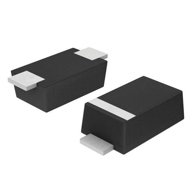
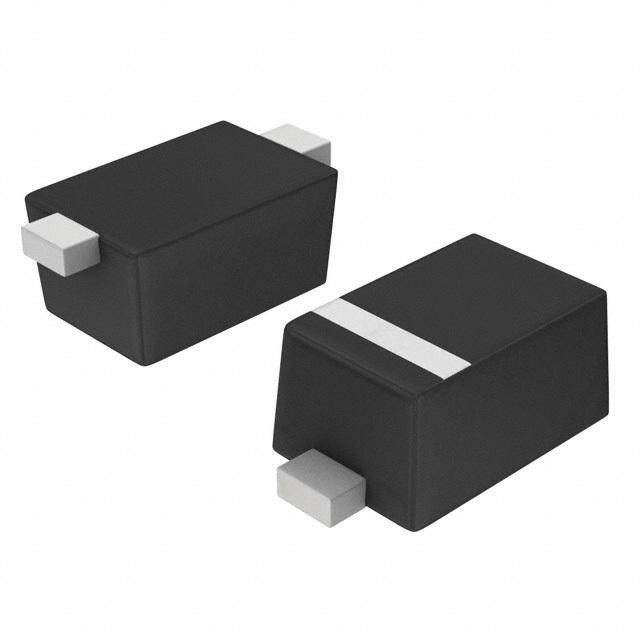
| 描述 | TVS DIODE 5.5VWM 6TSSOPESD 抑制器 2CHAN +/-8KV 0.9pF |
| 产品分类 | |
| 品牌 | NXP Semiconductors |
| 产品手册 | |
| 产品图片 |
|
| rohs | 符合RoHS无铅 / 符合限制有害物质指令(RoHS)规范要求 |
| 产品系列 | NXP Semiconductors IP4233CZ6,125- |
| 数据手册 | |
| 产品型号 | IP4233CZ6,125 |
| PCN封装 | |
| PCN设计/规格 | |
| 不同频率时的电容 | 0.9pF @ 1MHz |
| 产品种类 | ESD 抑制器 |
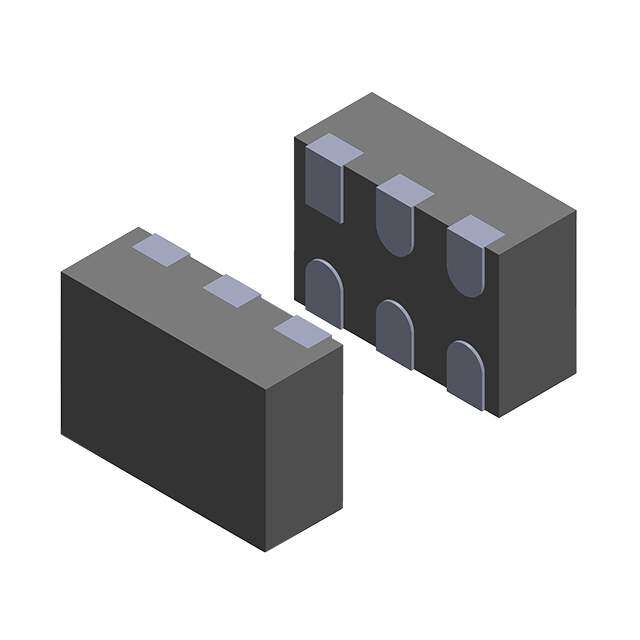
| 供应商器件封装 | 6-TSSOP |
| 其它名称 | 568-6852-6 |
| 击穿电压 | 6 V to 9.5 V |
| 功率-峰值脉冲 | - |
| 包装 | Digi-Reel® |
| 单向通道 | - |
| 双向通道 | 4 |
| 商标 | NXP Semiconductors |
| 安装类型 | 表面贴装 |
| 封装 | Reel |
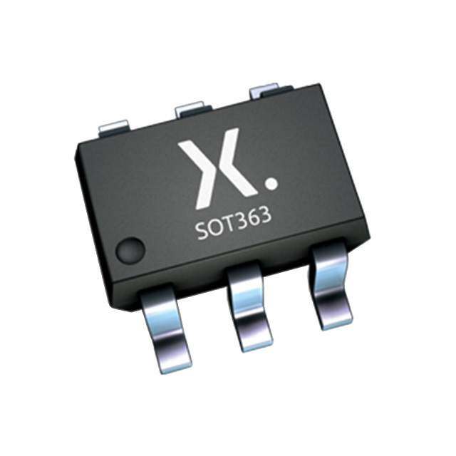
| 封装/外壳 | 6-TSSOP,SC-88,SOT-363 |
| 封装/箱体 | SC-88 |
| 工作温度 | -40°C ~ 85°C (TA) |
| 工作温度范围 | - 40 C to + 85 C |
| 工厂包装数量 | 3000 |
| 应用 | 以太网 |
| 标准包装 | 1 |
| 电压-击穿(最小值) | 6V |
| 电压-反向关态(典型值) | 5.5V |
| 电压-箝位(最大值)@Ipp | - |
| 电容 | 0.9 pF |
| 电流-峰值脉冲(10/1000µs) | - |
| 电源线路保护 | 无 |
| 端接类型 | SMD/SMT |
| 类型 | 转向装置(轨至轨) |
| 通道 | 2 Channels |


- 商务部:美国ITC正式对集成电路等产品启动337调查
- 曝三星4nm工艺存在良率问题 高通将骁龙8 Gen1或转产台积电
- 太阳诱电将投资9.5亿元在常州建新厂生产MLCC 预计2023年完工
- 英特尔发布欧洲新工厂建设计划 深化IDM 2.0 战略
- 台积电先进制程称霸业界 有大客户加持明年业绩稳了
- 达到5530亿美元!SIA预计今年全球半导体销售额将创下新高
- 英特尔拟将自动驾驶子公司Mobileye上市 估值或超500亿美元
- 三星加码芯片和SET,合并消费电子和移动部门,撤换高东真等 CEO
- 三星电子宣布重大人事变动 还合并消费电子和移动部门
- 海关总署:前11个月进口集成电路产品价值2.52万亿元 增长14.8%


PDF Datasheet 数据手册内容提取
IP4233CZ6 Ultra low capacitance ESD protection for Ethernet ports Rev. 3 — 17 June 2010 Product data sheet 1. Product profile 1.1 General description The IP4233CZ6 is designed to protect Input/Output(I/O) ports that are sensitive to capacitive loads, such as Ethernet, from destruction by ElectroStatic Discharge(ESD). The IP4233CZ6 incorporates two pairs of ultra low capacitance back-to-back diodes which protect components from ESD voltages as high as ±8kV contact discharge according to IEC61000-4-2, level4. The back-to-back diodes prevent negative clipping of AC signals and voltages below zero. The IP4233CZ6 is fabricated using monolithic silicon technology integrating two ultra low capacitance back-to-back ESDprotection diodes in a very small 6-lead SOT363 package. 1.2 Features and benefits (cid:132) Pb-free and Restriction of Hazardous Substances(RoHS) compliant (cid:132) ESDprotection compliant to IEC61000-4-2 level4, ±8kV contact discharge (cid:132) Two low input capacitance (0.9pF typical) back-to-back ESDprotection diodes (cid:132) Very small 6-lead SOT363 package 1.3 Applications (cid:132) ESD protection high-frequency AC-coupled Ethernet ports 1.4 Quick reference data Table 1. Quick reference data T =25°C unless otherwise specified. amb Symbol Parameter Conditions Min Typ Max Unit V electrostatic all pins; IEC61000-4-2, - -± 8 kV ESD discharge voltage level4; contact discharge C input/output to V =0V; f=1MHz [1][2] - 0.9 1.3 pF (I/O-GND) I groundcapacitance [1] Guaranteed by design. [2] Pins2 to6 and pins3 to5.
IP4233CZ6 Nexperia Ultra low capacitance ESD protection for Ethernet ports 2. Pinning information Table 2. Pinning Pin Description Simplified outline Graphic symbol 1 not connected 6 5 4 2 ESD protection I/O channel 1 1 6 3 ESD protection I/O channel 2 2 5 4 not connected 3 4 5 ESD protection I/O channel 2 1 2 3 018aaa013 6 ESD protection I/O channel 1 3. Ordering information Table 3. Ordering information Type number Package Name Description Version IP4233CZ6 SC-88 plastic surface-mounted package; 6leads SOT363 4. Limiting values Table 4. Limiting values In accordance with the Absolute Maximum Rating System (IEC 60134). Symbol Parameter Conditions Min Max Unit V input voltage - ±5.5 V I V electrostatic discharge all pins; IEC61000-4-2, - ±8 kV ESD voltage level4; contact discharge T storage temperature −55 +125 °C stg T ambient temperature −40 +85 °C amb 5. Characteristics Table 5. Characteristics T =25°C unless otherwise specified. amb Symbol Parameter Conditions Min Typ Max Unit C input/output to V =0V; f=1MHz [1][2] - 0.9 1.3 pF (I/O-GND) I groundcapacitance I reverse leakage current V =3.0V [2] - - 100 nA RM I V breakdown voltage back-to-back diode; 6 - 9.5 V BR I=5mA [1] Guaranteed by design. [2] Pins2 to6 and pins3 to5. IP4233CZ6 All information provided in this document is subject to legal disclaimers. . Product data sheet Rev. 3 — 17 June 2010 2 of 11 © Nexperia B.V. 2017. All rights reserved
IP4233CZ6 Nexperia Ultra low capacitance ESD protection for Ethernet ports 6. Application information A typical application for protecting a 10/100Mbit/s Ethernet transceiver against ESD is shown in Figure1. not used not used PTC TX+ TX+ PTC TX− 1 6 TX− 2 5 Primary-Secondary RJ45 10/100 Coordinating BASE-T 3 4 Elements (Opt) ETHERNET IP4233CZ6 PTC RX+ RX+ PTC RX− not used RX− not used REMI REMI REMI REMI VCC VCC GND 018aaa014 Fig 1. Typical application for ESD protection of a 10/100Mbit/s Ethernet transceiver IP4233CZ6 All information provided in this document is subject to legal disclaimers. . Product data sheet Rev. 3 — 17 June 2010 3 of 11 © Nexperia B.V. 2017. All rights reserved
IP4233CZ6 Nexperia Ultra low capacitance ESD protection for Ethernet ports 7. Package outline Plastic surface-mounted package; 6 leads SOT363 D B E A X y HE v M A 6 5 4 Q pin 1 index A A1 1 2 3 c e1 bp w M B Lp e detail X 0 1 2 mm scale DIMENSIONS (mm are the original dimensions) A1 UNIT A max bp c D E e e1 HE Lp Q v w y 1.1 0.30 0.25 2.2 1.35 2.2 0.45 0.25 mm 0.1 1.3 0.65 0.2 0.2 0.1 0.8 0.20 0.10 1.8 1.15 2.0 0.15 0.15 OUTLINE REFERENCES EUROPEAN ISSUE DATE VERSION IEC JEDEC JEITA PROJECTION 04-11-08 SOT363 SC-88 06-03-16 Fig 2. Package outline SOT363(SC-88) IP4233CZ6 All information provided in this document is subject to legal disclaimers. . Product data sheet Rev. 3 — 17 June 2010 4 of 11 © Nexperia B.V. 2017. All rights reserved
IP4233CZ6 Nexperia Ultra low capacitance ESD protection for Ethernet ports 8. Soldering of SMD packages This text provides a very brief insight into a complex technology. A more in-depth account of soldering ICs can be found in Application Note AN10365 “Surface mount reflow soldering description”. 8.1 Introduction to soldering Soldering is one of the most common methods through which packages are attached to Printed Circuit Boards (PCBs), to form electrical circuits. The soldered joint provides both the mechanical and the electrical connection. There is no single soldering method that is ideal for all IC packages. Wave soldering is often preferred when through-hole and Surface Mount Devices (SMDs) are mixed on one printed wiring board; however, it is not suitable for fine pitch SMDs. Reflow soldering is ideal for the small pitches and high densities that come with increased miniaturization. 8.2 Wave and reflow soldering Wave soldering is a joining technology in which the joints are made by solder coming from a standing wave of liquid solder. The wave soldering process is suitable for the following: • Through-hole components • Leaded or leadless SMDs, which are glued to the surface of the printed circuit board Not all SMDs can be wave soldered. Packages with solder balls, and some leadless packages which have solder lands underneath the body, cannot be wave soldered. Also, leaded SMDs with leads having a pitch smaller than ~0.6mm cannot be wave soldered, due to an increased probability of bridging. The reflow soldering process involves applying solder paste to a board, followed by component placement and exposure to a temperature profile. Leaded packages, packages with solder balls, and leadless packages are all reflow solderable. Key characteristics in both wave and reflow soldering are: • Board specifications, including the board finish, solder masks and vias • Package footprints, including solder thieves and orientation • The moisture sensitivity level of the packages • Package placement • Inspection and repair • Lead-free soldering versus SnPb soldering 8.3 Wave soldering Key characteristics in wave soldering are: • Process issues, such as application of adhesive and flux, clinching of leads, board transport, the solder wave parameters, and the time during which components are exposed to the wave • Solder bath specifications, including temperature and impurities IP4233CZ6 All information provided in this document is subject to legal disclaimers. . Product data sheet Rev. 3 — 17 June 2010 5 of 11 © Nexperia B.V. 2017. All rights reserved
IP4233CZ6 Nexperia Ultra low capacitance ESD protection for Ethernet ports 8.4 Reflow soldering Key characteristics in reflow soldering are: • Lead-free versus SnPb soldering; note that a lead-free reflow process usually leads to higher minimum peak temperatures (see Figure3) than a SnPb process, thus reducing the process window • Solder paste printing issues including smearing, release, and adjusting the process window for a mix of large and small components on one board • Reflow temperature profile; this profile includes preheat, reflow (in which the board is heated to the peak temperature) and cooling down. It is imperative that the peak temperature is high enough for the solder to make reliable solder joints (a solder paste characteristic). In addition, the peak temperature must be low enough that the packages and/or boards are not damaged. The peak temperature of the package depends on package thickness and volume and is classified in accordance with Table6 and7 Table 6. SnPb eutectic process (from J-STD-020C) Package thickness (mm) Package reflow temperature (°C) Volume (mm3) < 350 ≥ 350 < 2.5 235 220 ≥ 2.5 220 220 Table 7. Lead-free process (from J-STD-020C) Package thickness (mm) Package reflow temperature (°C) Volume (mm3) < 350 350 to 2000 > 2000 < 1.6 260 260 260 1.6 to 2.5 260 250 245 > 2.5 250 245 245 Moisture sensitivity precautions, as indicated on the packing, must be respected at all times. Studies have shown that small packages reach higher temperatures during reflow soldering, see Figure3. IP4233CZ6 All information provided in this document is subject to legal disclaimers. . Product data sheet Rev. 3 — 17 June 2010 6 of 11 © Nexperia B.V. 2017. All rights reserved
IP4233CZ6 Nexperia Ultra low capacitance ESD protection for Ethernet ports maximum peak temperature = MSL limit, damage level temperature minimum peak temperature = minimum soldering temperature peak temperature time 001aac844 MSL: Moisture Sensitivity Level Fig 3. Temperature profiles for large and small components For further information on temperature profiles, refer to Application Note AN10365 “Surface mount reflow soldering description”. IP4233CZ6 All information provided in this document is subject to legal disclaimers. . Product data sheet Rev. 3 — 17 June 2010 7 of 11 © Nexperia B.V. 2017. All rights reserved
IP4233CZ6 Nexperia Ultra low capacitance ESD protection for Ethernet ports 9. Revision history Table 8. Revision history Document ID Release date Data sheet status Change notice Supersedes IP4233CZ6 v.3 20100617 Product data sheet - IP4233CZ6 v.2 Modifications: • Figure1: corrected • Section 10 “Legal information”: updated IP4233CZ6 v.2 20100506 Preliminary data sheet - IP4233CZ6_1 IP4233CZ6_1 20090330 Objective data sheet - - IP4233CZ6 All information provided in this document is subject to legal disclaimers. . Product data sheet Rev. 3 — 17 June 2010 8 of 11 © Nexperia B.V. 2017. All rights reserved
IP4233CZ6 Nexperia Ultra low capacitance ESD protection for Ethernet ports 10. Legal information 10.1 Data sheet status Document status[1][2] Product status[3] Definition Objective [short] data sheet Development This document contains data from the objective specification for product development. Preliminary [short] data sheet Qualification This document contains data from the preliminary specification. Product [short] data sheet Production This document contains the product specification. [1] Please consult the most recently issued document before initiating or completing a design. [2] The term ‘short data sheet’ is explained in section “Definitions”. [3] The product status of device(s) described in this document may have changed since this document was published and may differ in case of multiple devices. The latest product status information is available on the Internet at URLhttp://www.nexperia.com. 10.2 Definitions malfunction of a Nexperia product can reasonably be expected to result in personal injury, death or severe property or environmental damage. Nexperia accepts no liability for inclusion and/or use of Draft — The document is a draft version only. The content is still under Nexperia products in such equipment or applications and internal review and subject to formal approval, which may result in therefore such inclusion and/or use is at the customer’s own risk. modifications or additions. Nexperia does not give any representations or warranties as to the accuracy or completeness of Applications — Applications that are described herein for any of these information included herein and shall have no liability for the consequences of products are for illustrative purposes only. Nexperia makes no use of such information. representation or warranty that such applications will be suitable for the specified use without further testing or modification. Short data sheet — A short data sheet is an extract from a full data sheet with the same product type number(s) and title. A short data sheet is intended Customers are responsible for the design and operation of their applications for quick reference only and should not be relied upon to contain detailed and and products using Nexperia products, and Nexperia full information. For detailed and full information see the relevant full data accepts no liability for any assistance with applications or customer product sheet, which is available on request via the local Nexperia sales design. It is customer’s sole responsibility to determine whether the Nexperia office. In case of any inconsistency or conflict with the short data sheet, the product is suitable and fit for the customer’s applications and full data sheet shall prevail. products planned, as well as for the planned application and use of customer’s third party customer(s). Customers should provide appropriate Product specification — The information and data provided in a Product design and operating safeguards to minimize the risks associated with their data sheet shall define the specification of the product as agreed between applications and products. Nexperia and its customer, unless Nexperia and Nexperia does not accept any liability related to any default, customer have explicitly agreed otherwise in writing. In no event however, damage, costs or problem which is based on any weakness or default in the shall an agreement be valid in which the Nexperia product is customer’s applications or products, or the application or use by customer’s deemed to offer functions and qualities beyond those described in the third party customer(s). Customer is responsible for doing all necessary Product data sheet. testing for the customer’s applications and products using Nexperia products in order to avoid a default of the applications and 10.3 Disclaimers the products or of the application or use by customer’s third party customer(s). Nexperia does not accept any liability in this respect. Limited warranty and liability — Information in this document is believed to Limiting values — Stress above one or more limiting values (as defined in be accurate and reliable. However, Nexperia does not give any the Absolute Maximum Ratings System of IEC60134) will cause permanent representations or warranties, expressed or implied, as to the accuracy or damage to the device. Limiting values are stress ratings only and (proper) completeness of such information and shall have no liability for the operation of the device at these or any other conditions above those given in consequences of use of such information. the Recommended operating conditions section (if present) or the Characteristics sections of this document is not warranted. Constant or In no event shall Nexperia be liable for any indirect, incidental, repeated exposure to limiting values will permanently and irreversibly affect punitive, special or consequential damages (including - without limitation - lost the quality and reliability of the device. profits, lost savings, business interruption, costs related to the removal or replacement of any products or rework charges) whether or not such Terms and conditions of commercial sale — Nexperia damages are based on tort (including negligence), warranty, breach of products are sold subject to the general terms and conditions of commercial contract or any other legal theory. sale, as published at http://www.nexperia.com/profile/terms, unless otherwise Notwithstanding any damages that customer might incur for any reason agreed in a valid written individual agreement. In case an individual whatsoever, Nexperia’s aggregate and cumulative liability towards agreement is concluded only the terms and conditions of the respective customer for the products described herein shall be limited in accordance agreement shall apply. Nexperia hereby expressly objects to with the Terms and conditions of commercial sale of Nexperia. applying the customer’s general terms and conditions with regard to the purchase of Nexperia products by customer. Right to make changes — Nexperia reserves the right to make changes to information published in this document, including without No offer to sell or license — Nothing in this document may be interpreted or limitation specifications and product descriptions, at any time and without construed as an offer to sell products that is open for acceptance or the grant, notice. This document supersedes and replaces all information supplied prior conveyance or implication of any license under any copyrights, patents or to the publication hereof. other industrial or intellectual property rights. Suitability for use — Nexperia products are not designed, Export control — This document as well as the item(s) described herein authorized or warranted to be suitable for use in life support, life-critical or may be subject to export control regulations. Export might require a prior safety-critical systems or equipment, nor in applications where failure or authorization from national authorities. IP4233CZ6 All information provided in this document is subject to legal disclaimers. . Product data sheet Rev. 3 — 17 June 2010 9 of 11 © Nexperia B.V. 2017. All rights reserved
IP4233CZ6 Nexperia Ultra low capacitance ESD protection for Ethernet ports Quick reference data — The Quick reference data is an extract of the product for such automotive applications, use and specifications, and (b) product data given in the Limiting values and Characteristics sections of this whenever customer uses the product for automotive applications beyond document, and as such is not complete, exhaustive or legally binding. Nexperia’s specifications such use shall be solely at customer’s own risk, and (c) customer fully indemnifies Nexperia for any Non-automotive qualified products — Unless this data sheet expressly liability, damages or failed product claims resulting from customer design and states that this specific Nexperia product is automotive qualified, use of the product for automotive applications beyond Nexperia’s the product is not suitable for automotive use. It is neither qualified nor tested standard warranty and Nexperia’s product specifications. in accordance with automotive testing or application requirements. Nexperia accepts no liability for inclusion and/or use of non-automotive qualified products in automotive equipment or applications. 10.4 Trademarks In the event that customer uses the product for design-in and use in automotive applications to automotive specifications and standards, customer Notice: All referenced brands, product names, service names and trademarks (a) shall use the product without Nexperia’s warranty of the are the property of their respective owners. 11. Contact information For more information, please visit: http://www.nexperia.com For sales office addresses, please send an email to: salesaddresses@nexperia.com IP4233CZ6 All information provided in this document is subject to legal disclaimers. . Product data sheet Rev. 3 — 17 June 2010 10 of 11 © Nexperia B.V. 2017. All rights reserved
IP4233CZ6 Nexperia Ultra low capacitance ESD protection for Ethernet ports 12. Contents 1 Product profile. . . . . . . . . . . . . . . . . . . . . . . . . . 1 1.1 General description . . . . . . . . . . . . . . . . . . . . . 1 1.2 Features and benefits. . . . . . . . . . . . . . . . . . . . 1 1.3 Applications . . . . . . . . . . . . . . . . . . . . . . . . . . . 1 1.4 Quick reference data . . . . . . . . . . . . . . . . . . . . 1 2 Pinning information. . . . . . . . . . . . . . . . . . . . . . 2 3 Ordering information. . . . . . . . . . . . . . . . . . . . . 2 4 Limiting values. . . . . . . . . . . . . . . . . . . . . . . . . . 2 5 Characteristics. . . . . . . . . . . . . . . . . . . . . . . . . . 2 6 Application information. . . . . . . . . . . . . . . . . . . 3 7 Package outline. . . . . . . . . . . . . . . . . . . . . . . . . 4 8 Soldering of SMD packages . . . . . . . . . . . . . . . 5 8.1 Introduction to soldering. . . . . . . . . . . . . . . . . . 5 8.2 Wave and reflow soldering. . . . . . . . . . . . . . . . 5 8.3 Wave soldering. . . . . . . . . . . . . . . . . . . . . . . . . 5 8.4 Reflow soldering. . . . . . . . . . . . . . . . . . . . . . . . 6 9 Revision history. . . . . . . . . . . . . . . . . . . . . . . . . 8 10 Legal information. . . . . . . . . . . . . . . . . . . . . . . . 9 10.1 Data sheet status . . . . . . . . . . . . . . . . . . . . . . . 9 10.2 Definitions. . . . . . . . . . . . . . . . . . . . . . . . . . . . . 9 10.3 Disclaimers. . . . . . . . . . . . . . . . . . . . . . . . . . . . 9 10.4 Trademarks. . . . . . . . . . . . . . . . . . . . . . . . . . . 10 11 Contact information. . . . . . . . . . . . . . . . . . . . . 10 12 Contents. . . . . . . . . . . . . . . . . . . . . . . . . . . . . . 11 © Nexperia B.V. 2017. All rights reserved For more information, please visit: http://www.nexperia.com For sales office addresses, please send an email to: salesaddresses@nexperia.com Date of release: 17 June 2010