 Datasheet下载
- 型号: SM15T12CA
- 制造商: STMicroelectronics
- 库位|库存: xxxx|xxxx
- 要求:
| 数量阶梯 | 香港交货 | 国内含税 |
| +xxxx | $xxxx | ¥xxxx |
查看当月历史价格
查看今年历史价格
SM15T12CA产品简介:
ICGOO电子元器件商城为您提供SM15T12CA由STMicroelectronics设计生产,在icgoo商城现货销售,并且可以通过原厂、代理商等渠道进行代购。 SM15T12CA价格参考¥2.01-¥2.01。STMicroelectronicsSM15T12CA封装/规格:TVS - 二极管, 21.7V Clamp 461A(8/20µs) Ipp Tvs Diode 表面贴装 SMC。您可以下载SM15T12CA参考资料、Datasheet数据手册功能说明书,资料中有SM15T12CA 详细功能的应用电路图电压和使用方法及教程。
STMicroelectronics的SM15T12CA是一款瞬态电压抑制(TVS)二极管,主要用于电路中的过电压保护。该器件可快速响应电压瞬变,吸收高能量浪涌,保护下游元件免受静电放电(ESD)、电感负载切换或雷击感应等引起的电压尖峰损害。

SM15T12CA的击穿电压约为12V,适用于直流电源线或信号线的保护,常见于工业控制设备、通信模块、消费电子产品及汽车电子中。例如,在工业自动化系统中,它可保护PLC输入输出端口;在通信设备中,可用于保护以太网接口或RS-485通信线路;在消费类电子产品中,常用于电源适配器输出端或USB接口的过压保护。此外,由于其较高的可靠性与稳定性,也适合用于环境较恶劣、电磁干扰较强的场合。
| 参数 | 数值 |
| 产品目录 | |
| 描述 | TVS DIODE 10.2VWM 21.7VC SMCTVS 二极管 - 瞬态电压抑制器 1500W 12V Bidirect |
| 产品分类 | |
| 品牌 | STMicroelectronics |
| 产品手册 | |
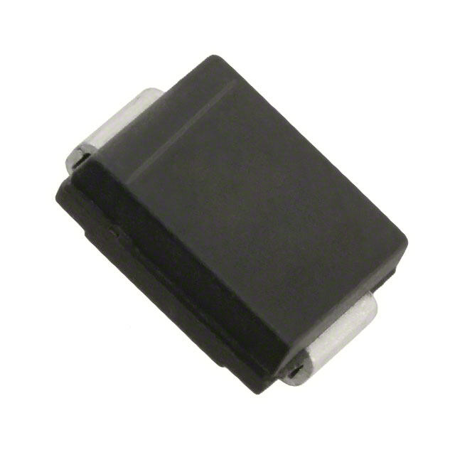
| 产品图片 |
|
| rohs | 符合RoHS无铅 / 符合限制有害物质指令(RoHS)规范要求 |
| 产品系列 | 二极管与整流器,TVS二极管,TVS 二极管 - 瞬态电压抑制器,STMicroelectronics SM15T12CASM15T, TRANSIL™ |
| 数据手册 | |
| 产品型号 | SM15T12CA |
| 不同频率时的电容 | - |
| 产品种类 | TVS 二极管 - 瞬态电压抑制器 |
| 供应商器件封装 | SMC |
| 其它名称 | 497-12771-6 |
| 其它有关文件 | http://www.st.com/web/catalog/sense_power/FM114/CL1460/SC235/PF64206?referrer=70071840 |
| 击穿电压 | 12 V |
| 功率-峰值脉冲 | 1500W (1.5kW) |
| 包装 | Digi-Reel® |
| 单向通道 | - |
| 双向通道 | 1 |
| 商标 | STMicroelectronics |
| 商标名 | Transil |
| 安装类型 | 表面贴装 |
| 安装风格 | SMD/SMT |
| 封装 | Reel |
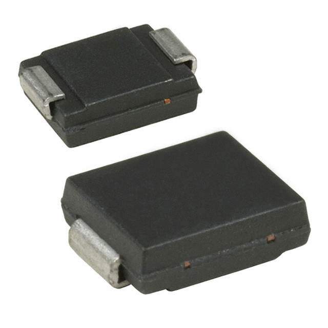
| 封装/外壳 | DO-214AB,SMC |
| 封装/箱体 | DO-214AB |
| 尺寸 | 6.25 mm W x 7.15 mm L x 2.45 mm H |
| 峰值浪涌电流 | 90 A |
| 峰值脉冲功率耗散 | 1.5 kW |
| 工作温度 | -55°C ~ 150°C (TJ) |
| 工作电压 | 10.2 V |
| 工厂包装数量 | 2500 |
| 应用 | 通用 |
| 最大工作温度 | + 150 C |
| 最小工作温度 | - 55 C |
| 极性 | Bidirectional |
| 标准包装 | 1 |
| 电压-击穿(最小值) | 11.4V |
| 电压-反向关态(典型值) | 10.2V |
| 电压-箝位(最大值)@Ipp | 21.7V |
| 电容 | 6000 pF |
| 电流-峰值脉冲(10/1000µs) | 461A (8/20µs) |
| 电源线路保护 | 无 |
| 端接类型 | SMD/SMT |
| 类型 | 齐纳 |
| 系列 | SM15T12 |
| 钳位电压 | 21.7 V |


- 商务部:美国ITC正式对集成电路等产品启动337调查
- 曝三星4nm工艺存在良率问题 高通将骁龙8 Gen1或转产台积电
- 太阳诱电将投资9.5亿元在常州建新厂生产MLCC 预计2023年完工
- 英特尔发布欧洲新工厂建设计划 深化IDM 2.0 战略
- 台积电先进制程称霸业界 有大客户加持明年业绩稳了
- 达到5530亿美元!SIA预计今年全球半导体销售额将创下新高
- 英特尔拟将自动驾驶子公司Mobileye上市 估值或超500亿美元
- 三星加码芯片和SET,合并消费电子和移动部门,撤换高东真等 CEO
- 三星电子宣布重大人事变动 还合并消费电子和移动部门
- 海关总署:前11个月进口集成电路产品价值2.52万亿元 增长14.8%


PDF Datasheet 数据手册内容提取
SM15T Transil™ Features ■ Peak pulse power: – 1500 W (10/1000 µs) – 10 kW (8/20 µs) ■ Breakdown voltage range: from 6.8 V to 220 V A ■ Unidirectional and bidirectional types ■ Low leakage current: – 0.2 µA at 25 °C K Unidirectional Bidirectional – 1 µA at 85 °C ■ Operating T : 150 °C j max SMC ■ High power capability at T : (JEDEC DO-214AB) jmax – 1250 W (10/1000 µs) ■ JEDEC registered package outline Complies with the following standards ■ IEC 61000-4-2 level 4 – 15 kV (air discharge) Description – 8 kV (contact discharge) ■ IEC 61000-4-5 The SM15T Transil series has been designed to – See Table3 for surge level protect sensitive equipment against electrostatic discharges according to IEC 61000-4-2, and ■ MIL STD 883G, method 3015-7: class 3B MIL STD 883, method 3015, and electrical over – 25 kV HBM (human body model) stress according to IEC 61000-4-4 and 5. These ■ UL 497B file number: QVGQ2.E136224 devices are more generally used against surges below 1500 W (10/1000µs). ■ Resin meets UL 94, V0 ■ MIL-STD-750, method 2026 soldererabilty Planar technology makes these devices suitable for high-end equipment and SMPS where low ■ EIA STD RS-481 and IEC 60286-3 packing leakage current and high junction temperature are ■ IPC 7531 footprint required to provide reliability and stability over time. SM15T are packaged in SMC (SMC footprint in accordance with IPC 7531 standard). TM: Transil is a trademark of STMicroelectronics September 2009 Doc ID 3080 Rev 6 1/10 www.st.com 10
Characteristics SM15T 1 Characteristics Table 1. A bsolute maximum ratings (T = 25 °C) amb Symbol Parameter Value Unit P Peak pulse power dissipation(1) T = T 1500 W PP jinitial amb T Storage temperature range -65 to + 150 °C stg T Operating junction temperature range -55 to + 150 °C j T Maximum lead temperature for soldering during 10 s. 260 °C L 1. For a surge greater than the maximum values, the diode will fail in short-circuit. Table 2. T hermal parameter Symbol Parameter Value Unit R Junction to leads 15 °C/W th(j-l) R Junction to ambient on printed circuit on recommended pad layout 90 °C/W th(j-a) Figure 1. Electrical characteristics - definitions II II Symbol Parameter VRM Stand-off voltage Unidirectional IIFF IIPPPP VBR Breakdown voltage VCL Clamping voltage II IRM Leakage current @VRM VVCCLLVVBBRRVVRRMM VVFF VV VVCCLLVVBBRRVVRRMM IIRRRRMM VV IαPTP PVoelatakg peu tlseem cpuerrraetnutre coefficient IIRIRIRRMM IIRRIIRRMM VVRRMMVVBBRRVVCCLL VF Forward voltage drop RD Dynamic resistance IIPPPP IIPPPP Bidirectional Figure 2. Pulse definition for electrical characteristics %IPP 100 Pulse waveform 50 tr = rise time (µs) tp = pulse duration time (µs) 0 t tr tp 2/10 Doc ID 3080 Rev 6
SM15T Characteristics Table 3. E lectrical characteristics, parameter values (T = 25 °C) amb R R V @I D V @I D I max@V V @I (1) CL PP 10/1000 CL PP 8/20 αT (2) RM RM BR R 10/1000µs 8/20µs µs µs Order code 25 °C 85 °C min typ max max max max µA V V mA V(3) A(4) Ω V(3) A(4) Ω 10-4/ °C SM15T6V8A/CA 500 2000 5.8 6.45 6.8 7.14 10 10.5 143 0.023 13.4 746 0.008 5.7 SM15T7V5A/CA 250 1000 6.4 7.13 7.5 7.88 10 11.3 132 0.026 14.5 690 0.010 6.1 SM15T10A/CA 10 50 8.55 9.5 10 10.5 1 14.5 103 0.039 18.6 538 0.015 7.3 SM15T12A/CA 0.2 1 10.2 11.4 12 12.6 1 16.7 90 0.046 21.7 461 0.020 7.8 SM15T15A/CA 0.2 1 12.8 14.3 15 15.8 1 21.2 71 0.076 27.2 368 0.031 8.4 SM15T18A/CA 0.2 1 15.3 17.1 18 18.9 1 25.2 59.5 0.106 32.5 308 0.044 8.8 SM15T22A/CA 0.2 1 18.8 20.9 22 23.1 1 30.6 49 0.153 39.3 254 0.064 9.2 SM15T24A/CA 0.2 1 20.5 22.8 24 25.2 1 33.2 45 0.178 42.8 234 0.075 9.4 SM15T27A/CA 0.2 1 23.1 25.7 27 28.4 1 37.5 40 0.228 48.3 207 0.096 9.6 SM15T30A/CA 0.2 1 25.6 28.5 30 31.5 1 41.5 36 0.278 53.5 187 0.12 9.7 SM15T33A/CA 0.2 1 28.2 31.4 33 34.7 1 45.7 33 0.333 59.0 169 0.14 9.8 SM15T36A/CA 0.2 1 30.8 34.2 36 37.8 1 49.9 30 0.403 64.3 156 0.17 9.9 SM15T39A/CA 0.2 1 33.3 37.1 39 41.0 1 53.9 28 0.461 69.7 143 0.20 10.0 SM15T68A/CA 0.2 1 58.1 64.6 68 71.4 1 92 16.3 1.26 121 83 0.60 10.4 SM15T75A/CA 0.2 1 64.1 71.3 75 78.8 1 103 14.6 1.66 134 75 0.74 10.5 SM15T100A/CA 0.2 1 85.5 95.0 100 105 1 137 11 2.91 178 56 1.30 10.6 SM15T150A/CA 0.2 1 128 143 150 158 1 207 7.2 6.81 265 38 2.82 10.8 SM15T200A/CA 0.2 1 171 190 200 210 1 274 5.5 11.6 353 28 5.11 10.8 SM15T220A/CA 0.2 1 188 209 220 231 1 328 4.6 21.1 388 26 6.04 10.8 1. Pulse test : t < 50 ms p 2. To calculate V versus junction temperature, use the following formula: V @ T = V @ 25°C x (1 + αT x (T – 25)). BR BR J BR J 3. To calculate maximum clamping voltage at other surge level, use the following formula: V = R x I + V CL D PP BRmax. 4. Surge capability given for both directions for unidirectional and bidirectional types. Doc ID 3080 Rev 6 3/10
Characteristics SM15T Figure 3. P eak pulse power dissipation Figure 4. Peak pulse power versus versus initial junction temperature exponential pulse duration (printed circuit board) Ppp(W) PPP(kW) 2000 100.0 10/1000µs Tjinitial = 25°C 1500 10.0 1000 1.0 500 Tj(°C) tp(ms) 0 0.1 0 25 50 75 100 125 150 175 1.0E-03 1.0E-02 1.0E-01 1.0E+00 1.0E+01 Figure 5. Clamping voltage versus peak pulse current (maximum values) IPP(A) 1000.0 Tjinitial=25 °C A 0 1 100.0 T A 15 8 M A V S 0 6 3 8/20 µs T T 5 5 1 1 M M S S 10.0 A 2 2 T 10/1000 µs 5 1 M A S 8 6 T 10 ms 1.0 15 A M 0 A 5 S 1 20 T 2 M15 5T VCL(V) S M1 S 0.1 1 10 100 1000 4/10 Doc ID 3080 Rev 6
SM15T Characteristics Figure 6. C apacitance versus reverse applied Figure 7. Capacitance versus reverse applied voltage (typical values, SM15TxxA) voltage (typical values, SM15TxxCA) C (nF) C (nF) 10.00 10.0 F=1 MHz F=1 MHz SM15T6V8A VoscT=j=3205m°VCRMS SM15T6V8CA VoscT=j=3205m°VCRMS SM15T15A 1.00 SM15T15CA SM15T30A 1.0 SM15T30CA SM15T68A 0.10 SM15T68CA SM15T200A VR(V) VR(V) SM15T200CA 0.01 0.1 1 10 100 1000 1 10 100 1000 Figure 8. P eak forward voltage drop versus Figure 9. Relative variation of thermal forward current (typical values) impedance junction to ambient versus pulse duration IFM(A) Zth(j-a)/Rth(j-a) 100.0 1.00 Recommendedpadlayout 10.0 Tj=125°C 0.10 Tj=25°C 1.0 VFM(V) tP(s) 0.1 0.01 0.0 0.5 1.0 1.5 2.0 2.5 1.0E-03 1.0E-02 1.0E-01 1.0E+00 1.0E+01 1.0E+02 1.0E+03 Figure 10. Thermal resistance junction to Figure 11. Leakage current versus junction ambient versus copper surface temperature (typical values) under each lead Rth(j-a)(°C/W) IR(nA) 100 1.0E+04 90 printed circuit board FR4, copper thickness = 35 µm 80 1.0E+03 70 VR=VRM 60 VRM< 10V 50 1.0E+02 40 30 1.0E+01 20 10 SCu(cm²) VVRMR=≥V1R0MV Tj(°C) 0 1.0E+00 0.0 0.5 1.0 1.5 2.0 2.5 3.0 3.5 4.0 4.5 5.0 25 50 75 100 125 150 Doc ID 3080 Rev 6 5/10
Ordering information scheme SM15T 2 Ordering information scheme Figure 12. Ordering information scheme SM 15T 100 CA Surface mount Surge rating 15 = 1500WTransil in SMC Breakdown voltage 100 = 100V Types CA = Bidirectional A = Unidirectional 6/10 Doc ID 3080 Rev 6
SM15T Package information 3 Package information ● Case: JEDEC DO-214AB molded plastic over planar junction ● Terminals: solder plated, solderable as per MIL-STD-750, Method 2026 ● Polarity: for unidirectional types the band indicates cathode ● Flammability: epoxy is rated UL 94, V0 ● RoHS package In order to meet environmental requirements, ST offers these devices in different grades of ECOPACK® packages, depending on their level of environmental compliance. ECOPACK® specifications, grade definitions and product status are available at: www.st.com. ECOPACK® is an ST trademark. T able 4. SMC dimensions Dimensions Ref. Millimeters Inches E1 Min. Max. Min. Max. A1 1.90 2.45 0.075 0.096 D A2 0.05 0.20 0.002 0.008 b 2.90 3.20 0.114 0.126 c 0.15 0.40 0.006 0.016 E D 5.55 6.25 0.218 0.246 A1 E 7.75 8.15 0.305 0.321 C A2 E1 6.60 7.15 0.260 0.281 E2 L b E2 4.40 4.70 0.173 0.185 L 0.75 1.50 0.030 0.059 Figure 13. S MC footprint dimensions in mm Figure 14. Marking layout(1) (inches) 1.54 5.11 1.54 (0.061) (0.201) (0.061) Cathode bar (unidirectionaldevicesonly) 3.14 e e: ECOPACK compliance (0.124) XXX: Marking x x x Z: Manufacturing location Y: Year WW: week z y ww 8.19 (0.322) 1. Marking layout can vary according to assembly location. Doc ID 3080 Rev 6 7/10
Package information SM15T T able 5. Marking Order code Marking Order code Marking SM15T6V8A MDE SM15T6V8CA BDE SM15T7V5A MDG SM15T7V5CA BDG SM15T10A MDP SM15T10CA BDP SM15T12A MDT SM15T12CA BDT SM15T15A MDX SM15T15CA BDX SM15T18A MEE SM15T18CA BEE SM15T22A MEK SM15T22CA BEK SM15T24A MEM SM15T24CA BEM SM15T27A MEP SM15T27CA BEP SM15T30A MER SM15T30CA BER SM15T33A MET SM15T33CA BET SM15T36A MEV SM15T36CA BEV SM15T39A MEX SM15T39CA BEX SM15T68A MFP SM15T68CA BFP SM15T75A MFO SM15T75CA BFO SM15T100A MFX SM15T100CA BFX SM15T150A MGK SM15T150CA BGK SM15T200A MGV SM15T200CA BGV SM15T220A MGX SM15T220CA BGX 8/10 Doc ID 3080 Rev 6
SM15T Ordering information 4 Ordering information T able 6. Ordering information Order code Marking Package Weight Base qty Delivery mode SM15TxxxA/CA(1) See Table5 on page8 SMC 0.25 g 2500 Tape and reel 1. Where xxx is nominal value of V and A or CA indicates unidirectional or bidirectional version. See BR Table3 for list of available devices and their order codes 5 Revision history T able 7. Document revision history Date Revision Description of changes September-2001 3B Last issue 19-Feb-2007 4 Peak pulse power Figure4 on page4 updated. Updated ECOPACK statement. Added R columns in D 04-Feb-2009 5 Table3. Updated characteristic curves, Figure3 to Figure11. 17-Sep-2009 6 Document updated for low leakage current. Doc ID 3080 Rev 6 9/10
SM15T Please Read Carefully: Information in this document is provided solely in connection with ST products. STMicroelectronics NV and its subsidiaries (“ST”) reserve the right to make changes, corrections, modifications or improvements, to this document, and the products and services described herein at any time, without notice. All ST products are sold pursuant to ST’s terms and conditions of sale. Purchasers are solely responsible for the choice, selection and use of the ST products and services described herein, and ST assumes no liability whatsoever relating to the choice, selection or use of the ST products and services described herein. No license, express or implied, by estoppel or otherwise, to any intellectual property rights is granted under this document. If any part of this document refers to any third party products or services it shall not be deemed a license grant by ST for the use of such third party products or services, or any intellectual property contained therein or considered as a warranty covering the use in any manner whatsoever of such third party products or services or any intellectual property contained therein. UNLESS OTHERWISE SET FORTH IN ST’S TERMS AND CONDITIONS OF SALE ST DISCLAIMS ANY EXPRESS OR IMPLIED WARRANTY WITH RESPECT TO THE USE AND/OR SALE OF ST PRODUCTS INCLUDING WITHOUT LIMITATION IMPLIED WARRANTIES OF MERCHANTABILITY, FITNESS FOR A PARTICULAR PURPOSE (AND THEIR EQUIVALENTS UNDER THE LAWS OF ANY JURISDICTION), OR INFRINGEMENT OF ANY PATENT, COPYRIGHT OR OTHER INTELLECTUAL PROPERTY RIGHT. UNLESS EXPRESSLY APPROVED IN WRITING BY AN AUTHORIZED ST REPRESENTATIVE, ST PRODUCTS ARE NOT RECOMMENDED, AUTHORIZED OR WARRANTED FOR USE IN MILITARY, AIR CRAFT, SPACE, LIFE SAVING, OR LIFE SUSTAINING APPLICATIONS, NOR IN PRODUCTS OR SYSTEMS WHERE FAILURE OR MALFUNCTION MAY RESULT IN PERSONAL INJURY, DEATH, OR SEVERE PROPERTY OR ENVIRONMENTAL DAMAGE. ST PRODUCTS WHICH ARE NOT SPECIFIED AS "AUTOMOTIVE GRADE" MAY ONLY BE USED IN AUTOMOTIVE APPLICATIONS AT USER’S OWN RISK. Resale of ST products with provisions different from the statements and/or technical features set forth in this document shall immediately void any warranty granted by ST for the ST product or service described herein and shall not create or extend in any manner whatsoever, any liability of ST. ST and the ST logo are trademarks or registered trademarks of ST in various countries. Information in this document supersedes and replaces all information previously supplied. The ST logo is a registered trademark of STMicroelectronics. All other names are the property of their respective owners. © 2009 STMicroelectronics - All rights reserved STMicroelectronics group of companies Australia - Belgium - Brazil - Canada - China - Czech Republic - Finland - France - Germany - Hong Kong - India - Israel - Italy - Japan - Malaysia - Malta - Morocco - Philippines - Singapore - Spain - Sweden - Switzerland - United Kingdom - United States of America www.st.com 10/10 Doc ID 3080 Rev 6
Mouser Electronics Authorized Distributor Click to View Pricing, Inventory, Delivery & Lifecycle Information: S TMicroelectronics: SM15T150CA SM15T75A SM15T6V8CA SM15T27A SM15T24A SM15T68A SM15T22A SM15T33CA SM15T200A SM15T12CA SM15T36CA SM15T24CA SM15T22CA SM15T220A SM15T7V5A SM15T68CA SM15T18CA SM15T33A SM15T30A SM15T36A SM15T39A SM15T39CA SM15T18A SM15T10A SM15T12A SM15T100CA SM15T6V8A SM15T10CA SM15T100A SM15T200CA SM15T220CA SM15T15A SM15T15CA SM15T30CA SM15T7V5CA