 Datasheet下载
- 型号: 1SMB18CAT3G
- 制造商: ON Semiconductor
- 库位|库存: xxxx|xxxx
- 要求:
| 数量阶梯 | 香港交货 | 国内含税 |
| +xxxx | $xxxx | ¥xxxx |
查看当月历史价格
查看今年历史价格
1SMB18CAT3G产品简介:
ICGOO电子元器件商城为您提供1SMB18CAT3G由ON Semiconductor设计生产,在icgoo商城现货销售,并且可以通过原厂、代理商等渠道进行代购。 1SMB18CAT3G价格参考。ON Semiconductor1SMB18CAT3G封装/规格:TVS - 二极管, 。您可以下载1SMB18CAT3G参考资料、Datasheet数据手册功能说明书,资料中有1SMB18CAT3G 详细功能的应用电路图电压和使用方法及教程。
1SMB18CAT3G 是 Littelfuse Inc. 生产的一款表面贴装 TVS(瞬态电压抑制)二极管,主要用于保护电子电路免受静电放电(ESD)、浪涌和其它瞬态电压的损害。该器件具有快速响应时间和低钳位电压特性,适用于对敏感电子元件进行高效保护。

其典型应用场景包括:

1. 通信设备:用于以太网、USB接口、HDMI等高速数据线路中,防止因静电或雷击引起的电压突变损坏芯片。
2. 工业控制系统:在PLC、传感器、自动化设备中提供电源与信号线的瞬态保护。
3. 消费电子产品:如智能手机、平板电脑、笔记本电脑中,用于保护充电口、数据接口及内部敏感IC。
4. 汽车电子系统:可用于车载娱乐系统、ECU模块、CAN总线通信等场景中的电路保护。
5. 电源管理模块:在AC/DC或DC/DC转换器中作为输入端保护器件,提升系统稳定性与可靠性。

综上,1SMB18CAT3G广泛应用于需要高可靠性和稳定性的电子系统中,尤其适合于空间受限且要求高性能保护的表面贴装设计。
| 参数 | 数值 |
| 产品目录 | |
| 描述 | TVS DIODE 18VWM 29.2VC SMBTVS 二极管 - 瞬态电压抑制器 18V 600W Bidirectional |
| 产品分类 | |
| 品牌 | ON Semiconductor |
| 产品手册 | |
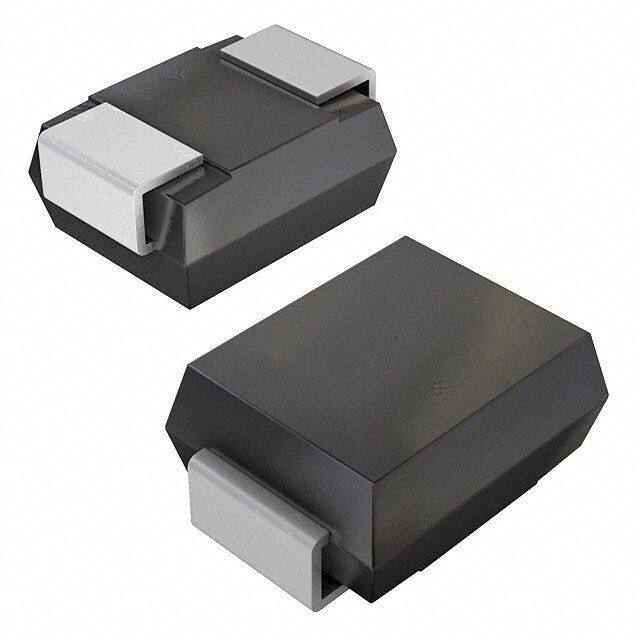
| 产品图片 |
|
| rohs | 符合RoHS无铅 / 符合限制有害物质指令(RoHS)规范要求 |
| 产品系列 | 二极管与整流器,TVS二极管,TVS 二极管 - 瞬态电压抑制器,ON Semiconductor 1SMB18CAT3G- |
| 数据手册 | |
| 产品型号 | 1SMB18CAT3G |
| 不同频率时的电容 | 465pF @ 1MHz |
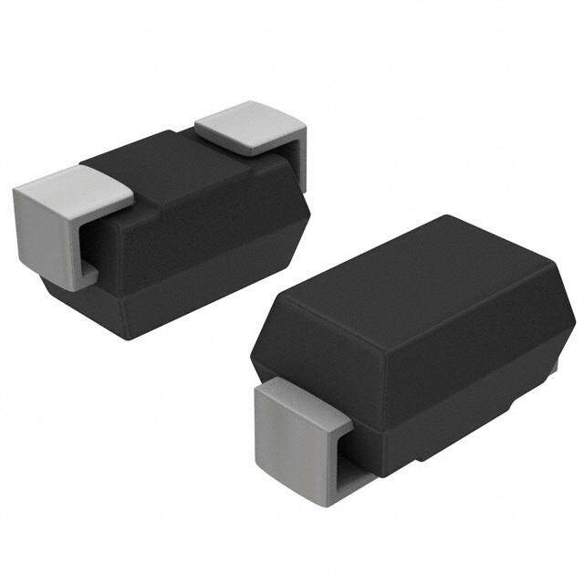
| 产品目录绘图 |
|
| 产品目录页面 | |
| 产品种类 | TVS 二极管 - 瞬态电压抑制器 |
| 供应商器件封装 | SMB |
| 其它名称 | 1SMB18CAT3GOSCT |
| 击穿电压 | 20 V |
| 功率-峰值脉冲 | 600W |
| 包装 | 剪切带 (CT) |
| 单向通道 | - |
| 双向通道 | 1 |
| 商标 | ON Semiconductor |
| 安装类型 | 表面贴装 |
| 安装风格 | SMD/SMT |
| 封装 | Reel |
| 封装/外壳 | DO-214AA,SMB |
| 封装/箱体 | DO-214AA |
| 尺寸 | 3.95 mm W x 4.6 mm L x 2.45 mm H |
| 峰值浪涌电流 | 20.5 A |
| 峰值脉冲功率耗散 | 600 W |
| 工作温度 | -65°C ~ 150°C (TJ) |
| 工作电压 | 18 V |
| 工厂包装数量 | 2500 |
| 应用 | 通用 |
| 最大工作温度 | + 150 C |
| 最小工作温度 | - 65 C |
| 极性 | Bidirectional |
| 标准包装 | 1 |
| 电压-击穿(最小值) | 20V |
| 电压-反向关态(典型值) | 18V |
| 电压-箝位(最大值)@Ipp | 29.2V |
| 电流-峰值脉冲(10/1000µs) | - |
| 电源线路保护 | 无 |
| 端接类型 | SMD/SMT |
| 类型 | 齐纳 |
| 系列 | 1SMB10CAT3G |
| 钳位电压 | 29.2 V |


- 商务部:美国ITC正式对集成电路等产品启动337调查
- 曝三星4nm工艺存在良率问题 高通将骁龙8 Gen1或转产台积电
- 太阳诱电将投资9.5亿元在常州建新厂生产MLCC 预计2023年完工
- 英特尔发布欧洲新工厂建设计划 深化IDM 2.0 战略
- 台积电先进制程称霸业界 有大客户加持明年业绩稳了
- 达到5530亿美元!SIA预计今年全球半导体销售额将创下新高
- 英特尔拟将自动驾驶子公司Mobileye上市 估值或超500亿美元
- 三星加码芯片和SET,合并消费电子和移动部门,撤换高东真等 CEO
- 三星电子宣布重大人事变动 还合并消费电子和移动部门
- 海关总署:前11个月进口集成电路产品价值2.52万亿元 增长14.8%


PDF Datasheet 数据手册内容提取
TVS Diodes Surface Mount > 600W > 1SMB10CAT3G Series 1SMB10CAT3G Series Pb Description The 1SMB10CAT3Gv series is designed to protect voltage sensitive components from high voltage, high energy transients. They have excellent clamping capability, high surge capability, low zener impedance and fast response time. The 1SMB10CAT3G series is supplied in the Littelfuse exclusive, cost-effective, highly reliable package and is ideally suited for use in communication systems, automotive, numerical controls, process controls, medical equipment, business machines, power supplies and many other industrial/consumer applications. Features • Working Peak Reverse Voltage Range − 10 V to 75 V Maximum Ratings and Thermal Characteristics • Standard Zener Breakdown Voltage Range − 11.7 V to 91.7 V Parameter Symbol Value Unit • Peak Power − 600 Watts @ 1 ms Peak Power Dissipation (Note 1) @ T = L P 600 W 25°C, Pulse Width = 1 ms PK • ESD Rating of Class 3 (> 16 kV) per Human Body Model • Maximum Clamp Voltage @ Peak Pulse Current DC Power Dissipation @ TL = 75°C PD 3.0 W Measured Zero Lead Length (Note 2) • Low Leakage < 5 µA Above 10 V Derate Above 75°C 40 mW/°C • UL 497B for Isolated Loop Circuit Protection Thermal Resistance from Junction− R JL 25 °C/W to−Lead Bi-directional • Response Time is Typically < 1 ns • Pb−Free Packages are Available DC Power Dissipation (Note 3) @ TA = P 0.55 W D 25°C Derate Above 25°C 4.4 mW/°C Thermal Resistance from Junction–to– 226 °C/W Functional Diagram Ambient R θJA Cathode Anode Operating and Storage -65 to T T °C Temperature Range J, stg +150 Stresses exceeding Maximum Ratings may damage the device. Maximum Ratings are stress ratings only. Functional operation above the Recommended Operating Conditions is Additional Information not implied. Extended exposure to stresses above the Recommended Operating Conditions Uni-directional may affect device reliability. 1. 10 X 1000 µs, non−repetitive 2. 1” square copper pad, FR−4 board 3. FR−4 board, using Littelfuse minimum recommended footprint, as shown in 403A-03 case outline dimensions spec *Please see 1SMB5.0AT3 to 1SMB170AT3 for Unidirectional devices Datasheet Resources Samples © 2017 Littelfuse, Inc. Specifications are subject to change without notice. Revised: 11/17/17
TVS Diodes Surface Mount > 600W > 1SMB10CAT3G Series I-V Curve Characteristics (T = 25°C unless otherwise noted) A Symbol Parameter IPP IPP Maximum Reverse Peak Pulse Current V Clamping Voltage @ I C PP IT VRWM Working Peak Reverse Voltage VC VBR VRWM IR I Maximum Reverse Leakage Current @ V IR VRWM VBR VC R RWM IT V Breakdown Voltage @ I BR T I Test Current T IPP © 2017 Littelfuse, Inc. Specifications are subject to change without notice. Revised: 11/17/17
TVS Diodes Surface Mount > 600W > 1SMB10CAT3G Series Electrical Characteristics V @ I V I @ Breakdown Voltage C PP (Note 8) RWM R C Typ. Device (Note 6) V Device* Marking RWM VBR @ IT (V) (Note 7) @ IT VC IPP (Note 9) Volts µA MIN NOM MAX mA Volts Amps pF 1SMB10CAT3G KXC 10 5.0 11.1 11.69 12.27 1.0 17.0 35.3 805 1SMB11CAT3G KZC 11 5.0 12.2 12.84 13.5 1.0 18.2 33.0 740 1SMB12CAT3G LEC 12 5.0 13.3 14.00 14.7 1.0 19.9 30.2 680 1SMB13CAT3G LGC 13 5.0 14.4 15.16 15.9 1.0 21.5 27.9 630 1SMB14CAT3G LKC 14 5.0 15.6 16.42 17.2 1.0 23.2 25.8 590 1SMB15CAT3G LMC 15 5.0 16.7 17.58 18.5 1.0 24.4 24.0 555 1SMB16CAT3G LPC 16 5.0 17.8 18.74 19.7 1.0 26.0 23.1 520 1SMB17CAT3G LRC 17 5.0 18.9 19.90 20.9 1.0 27.6 21.7 490 1SMB18CAT3G LTC 18 5.0 20.0 21.06 22.1 1.0 29.2 20.5 465 1SMB20CAT3G LVC 20 5.0 22.2 23.37 24.5 1.0 32.4 18.5 425 1SMB22CAT3G LXC 22 5.0 24.4 25.69 27.0 1.0 35.5 16.9 390 1SMB24CAT3G LZC 24 5.0 26.7 28.11 29.5 1.0 38.9 15.4 366 1SMB26CAT3G MEC 26 5.0 28.9 30.42 31.9 1.0 42.1 14.2 330 1SMB28CAT3G MGC 28 5.0 31.1 32.74 34.4 1.0 45.4 13.2 310 1SMB30CAT3G MKC 30 5.0 33.3 35.06 36.8 1.0 48.4 12.4 290 1SMB33CAT3G MMC 33 5.0 36.7 38.63 40.6 1.0 53.3 11.3 265 1SMB36CAT3G MPC 36 5.0 40.0 42.11 44.2 1.0 58.1 10.3 245 1SMB40CAT3G MRC 40 5.0 44.4 46.74 49.1 1.0 64.5 9.3 220 1SMB43CAT3G MTC 43 5.0 47.8 50.32 52.8 1.0 69.4 8.6 210 1SMB45CAT3G MVC 45 5.0 50.0 52.63 55.3 1.0 72.2 8.3 200 1SMB48CAT3G MXC 48 5.0 53.3 56.11 58.9 1.0 77.4 7.7 190 1SMB51CAT3G MZC 51 5.0 56.7 59.69 62.7 1.0 82.4 7.3 175 1SMB54CAT3G NEC 54 5.0 60.0 63.16 66.32 1.0 87.1 6.9 170 1SMB58CAT3G NGC 58 5.0 64.4 67.79 71.18 1.0 93.6 6.4 155 1SMB60CAT3G NKC 60 5.0 66.7 70.21 73.72 1.0 96.8 6.2 150 1SMB64CAT3G NMC 64 5.0 71.1 74.84 78.58 1.0 103 5.8 145 1SMB75CAT3G NRC 75 5.0 83.3 91.65 92.07 1.0 121 4.9 125 4. A transient suppressor is normally selected according to the working peak reverse voltage (V ), which should be equal to or greater than the RWM DC or continuous peak operating voltage level. 5. V measured at pulse test current I at an ambient temperature of 25°C. BR T 6. Surge current waveform per Figure 2 and derate per Figure 3 of the General Data − 600 Watt at the beginning of this group. 7. Bias Voltage = 0 V, F = 1 MHz, T = 25°C J © 2017 Littelfuse, Inc. Specifications are subject to change without notice. Revised: 11/17/17
TVS Diodes Surface Mount > 600W > 1SMB10CAT3G Series Ratings and Characteristic Curves Figure 1. Pulse Rating Curve Figure 2. Pulse Waveform 100 NONREPETITIVE PULSE WAVEFORM SHOWN IN FIGURE 2 10 1 0.1 0.1 s1 s1 0 s 100 s 1 ms 10 ms t Figure 3. Pulse Derating Curve Figure 4. Typical Junction Capacitance vs. Bias Voltage Typical Protection Circuit in in © 2017 Littelfuse, Inc. Specifications are subject to change without notice. Revised: 11/17/17
TVS Diodes Surface Mount > 600W > 1SMB10CAT3G Series Application Notes Response Time Figure 5. In most applications, the transient suppressor device is placed in parallel with the equipment or component to be protected. In this situation, there is a time delay associated with the capacitance of the device and an overshoot condition associated with the inductance of the device and the inductance of the connection method. The capacitive effect is of minor importance in the parallel protection scheme because it only produces a time delay in the transition from the operating voltage to the clamp voltage as shown in Figure 5. The inductive effects in the device are due to actual turn-on time (time required for the device to go from zero current to full current) and lead inductance. This inductive effect produces an overshoot in the voltage across the equipment or component being protected as shown in Figure 6. Minimizing this overshoot is very important in the application, since the main purpose for adding a transient Figure 6. suppressor is to clamp voltage spikes. The SMB series have a very good response time, typically < 1 ns and negligible inductance. However, external inductive effects could produce unacceptable overshoot. Proper circuit layout minimum lead lengths and placing the suppressor device as close as possible to the equipment or components to be protected will minimize this overshoot. Some input impedance represented by Zin is essential to prevent overstress of the protection device. This impedance should be as high as possible, without restricting the circuit operation. Duty Cycle Derating The data of Figure 1 applies for non-repetitive conditions and at a lead temperature of 25ºC. If the duty cycle increases, the peak power must be reduced as indicated by the curves of Figure 7. Average power must be derated Figure 7. Typical Derating Factor for Duty Cycle as the lead or ambient temperature rises above 25ºC. The average power derating curve normally given on data sheets may be normalized and used for this purpose. At first glance the derating curves of Figure 7 appear to be in error as the 10 ms pulse has a higher derating factor than the 10 s pulse. However, when the derating factor for a given pulse of Figure 7 is multiplied by the peak power value of Figure 1 for the same pulse, the results follow the expected trend. © 2017 Littelfuse, Inc. Specifications are subject to change without notice. Revised: 11/17/17
TVS Diodes Surface Mount > 600W > 1SMB10CAT3G Series Dimensions Soldering Footrpint HE E bD D POLARITY INDICATOR OPTIONAL AS NEEDED (SEE STYLES) A A1 mm L c inches Inches Millimeters ORDERING INFORMATION Dim Min Nom Max Min Nom Max Device Package Shipping A 0.075 0.087 0.090 1.90 2.20 2.28 A1 0.002 0.004 0.007 0.05 0.10 0.19 SMB 2,500 / 1SMBxxCAT3G (Pb−Free) Tape & Reel b 0.077 0.080 0.087 1.96 2.03 2.20 c 0.006 0.009 0.012 0.15 0.23 0.31 D 0.130 0.140 0.156 3.30 3.56 3.95 E 0.160 0.170 0.181 4.06 4.32 4.60 Flow/Wave Soldering (Solder Dipping) H 0.205 0.214 0.220 5.21 5.44 5.60 E L 0.030 0.040 0.063 0.76 1.02 1.60 Peak Temperature : 260 ºC L1 0.020 REF 0.51 REF Dipping Time : 10 seconds NOTES: 1. DIMENSIONING AND TOLERANCING PER ANSI Y14.5M, 1982. Physical Specifications 2. CONTROLLING DIMENSION: INCH. 3. D DIMENSION SHALL BE MEASURED WITHIN DIMENSION P. Void-free, transfer-molded, thermosetting Case plastic Part Marking System Polarity Cathode indicated by polarity band Mounting Position Any All external surfaces are corrosion Finish resistant and leads are readily solderable Modified L−Bend providing more contact Leads area to bond pads Disclaimer Notice - Information furnished is believed to be accurate and reliable. However, users should independently evaluate the suitability of and test each product selected for their own applications. Littelfuse products are not designed for, and may not be used in, all applications. Read complete Disclaimer Notice at: www.littelfuse.com/disclaimer-electronics. © 2017 Littelfuse, Inc. Specifications are subject to change without notice. Revised: 11/17/17