 Datasheet下载
- 型号: SMLJ36CA
- 制造商: Bourns
- 库位|库存: xxxx|xxxx
- 要求:
| 数量阶梯 | 香港交货 | 国内含税 |
| +xxxx | $xxxx | ¥xxxx |
查看当月历史价格
查看今年历史价格
SMLJ36CA产品简介:
ICGOO电子元器件商城为您提供SMLJ36CA由Bourns设计生产,在icgoo商城现货销售,并且可以通过原厂、代理商等渠道进行代购。 SMLJ36CA价格参考¥2.01-¥2.01。BournsSMLJ36CA封装/规格:TVS - 二极管, 。您可以下载SMLJ36CA参考资料、Datasheet数据手册功能说明书,资料中有SMLJ36CA 详细功能的应用电路图电压和使用方法及教程。
SMLJ36CA是Bourns Inc.生产的TVS(瞬态电压抑制)二极管,主要应用于电子设备中提供过电压保护。以下是其典型应用场景:

1. 消费电子产品:如智能手机、平板电脑、笔记本电脑等便携式设备。这些设备中的敏感电路容易受到静电放电(ESD)、雷击感应和电源浪涌的影响,SMLJ36CA可以有效地保护内部电路免受这些瞬态电压的损害。

2. 通信设备:包括路由器、调制解调器、交换机等网络设备。这些设备通常需要在复杂的电磁环境中工作,可能面临各种类型的电压瞬变。SMLJ36CA能够快速响应并抑制这些瞬变,确保设备的稳定运行。

3. 工业自动化系统:如可编程逻辑控制器(PLC)、传感器、执行器等。工业环境中存在大量的电气噪声和干扰源,SMLJ36CA可以保护这些关键组件不受损坏,提高系统的可靠性和安全性。

4. 汽车电子:例如车载信息娱乐系统、发动机控制单元(ECU)、安全气囊控制系统等。汽车环境中的电气系统可能会遭受电池反接、负载突降等异常情况,SMLJ36CA能够在这些情况下提供有效的保护,确保车辆电子系统的正常运作。

5. 医疗设备:如心电图仪、超声波设备、监护仪等。医疗设备对可靠性要求极高,任何瞬态电压都可能导致设备故障或数据丢失,影响诊断和治疗效果。SMLJ36CA可以帮助保护这些设备的关键电路,保障患者的安全和诊疗的准确性。

总之,SMLJ36CA作为一种高性能的TVS二极管,广泛应用于各类电子设备中,为敏感电路提供可靠的过电压保护,确保设备在复杂多变的电气环境中稳定运行。
| 参数 | 数值 |
| 产品目录 | |
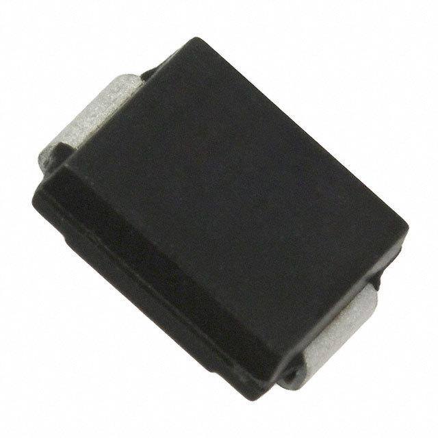
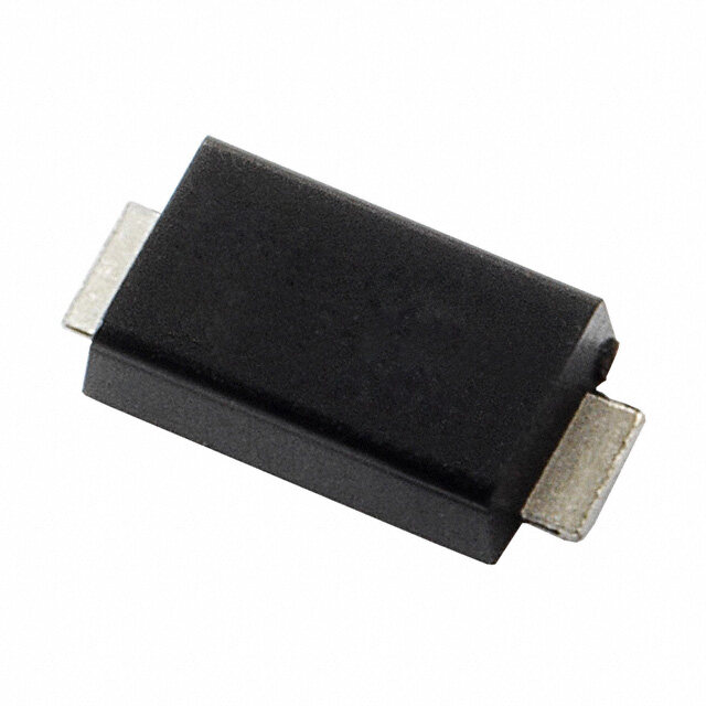
| 描述 | TVS DIODE 36VWM SMD |
| 产品分类 | |
| 品牌 | Bourns Inc. |
| 数据手册 | |
| 产品图片 |
|
| 产品型号 | SMLJ36CA |
| rohs | 不受无铅要求限制 / 符合限制有害物质指令(RoHS)规范要求 |
| RoHS指令信息 | |
| 产品系列 | SMLJ |
| 不同频率时的电容 | - |
| 产品目录绘图 |
|
| 产品目录页面 | |
| 供应商器件封装 | SMC (DO-214AB) |
| 其它名称 | SMLJ36CABTR |
| 功率-峰值脉冲 | 3000W (3kW) |
| 包装 | 带卷 (TR) |
| 单向通道 | - |
| 双向通道 | 1 |
| 安装类型 | 表面贴装 |
| 封装/外壳 | DO-214AB,SMC |
| 工作温度 | -55°C ~ 150°C (TJ) |
| 应用 | 通用 |
| 标准包装 | 3,000 |
| 特色产品 | http://www.digikey.com/product-highlights/cn/zh/bourns-smx-tvs-diodes/1448 |
| 电压-击穿(最小值) | 40V |
| 电压-反向关态(典型值) | 36V |
| 电压-箝位(最大值)@Ipp | - |
| 电流-峰值脉冲(10/1000µs) | - |
| 电源线路保护 | 无 |
| 类型 | 齐纳 |


- 商务部:美国ITC正式对集成电路等产品启动337调查
- 曝三星4nm工艺存在良率问题 高通将骁龙8 Gen1或转产台积电
- 太阳诱电将投资9.5亿元在常州建新厂生产MLCC 预计2023年完工
- 英特尔发布欧洲新工厂建设计划 深化IDM 2.0 战略
- 台积电先进制程称霸业界 有大客户加持明年业绩稳了
- 达到5530亿美元!SIA预计今年全球半导体销售额将创下新高
- 英特尔拟将自动驾驶子公司Mobileye上市 估值或超500亿美元
- 三星加码芯片和SET,合并消费电子和移动部门,撤换高东真等 CEO
- 三星电子宣布重大人事变动 还合并消费电子和移动部门
- 海关总署:前11个月进口集成电路产品价值2.52万亿元 增长14.8%


PDF Datasheet 数据手册内容提取
NT *RoHS VCEOARVMSIAPILOLINAASB LE Features Applications NT MPLIA n RoHS compliant* n IEC 61000-4-2 ESD (Min. Level 4) O HS C n Surface Mount SMC package n IEC 61000-4-4 EFT Ro * n Standoff Voltage: 5.0 to 170 volts n IEC 61000-4-5 Surge n Power Dissipation: 3000 watts REE D F LEA SMLJ Transient Voltage Suppressor Diode Series General Information TiBnhoceure rmnassa irnokgfefeltysr s so mTf rapalonlerstrai eebnlleet c Vctrooolmtnaimgc euc onSmiucapptpoiornenessns,t oscLr.VoER EADomRDH SIiSF poORCNuEdOSE teMAiPnsRLIEg Af NoaTr*n sdu vrgidee aon edq EuiSpDm epnrot taercet iochna allpepnlgicinagtio tnhse, sine mcoicmopnadcutc ctohri pin pdaucsktrayg teo DdOev-e2l1o4pA B (SMC) size format. The Transient Voltage Suppressor series offers a choice of Working Peak Reverse Voltage from 5 V up to 170 V and Breakdown Voltage up to 200 V. Typical fast response times are less than 1.0 ps for unidirectional devices and less than 5.0 ps for bidirectional devices from 0 V to Minimum Breakdown Voltage. Bourns® Chip Diodes conform to JEDEC standards, are easy to handle with standard pick and place equipment and the flat configuration minimizes roll away. Electrical Characteristics (@ TA = 25 °C Unless Otherwise Noted) Parameter Symbol Value Unit Minimum Peak Pulse Power Dissipation (TP = 1 ms) (Note 1,2) PPK 3000 Watts Peak Forward Surge Current 8.3 ms Single Half Sine Wave Superimposed on Rated Load IFSM 300 Amps (JEDEC Method) (Note 3) Steady State Power Dissipation @ TL = 75 °C PM(AV) 5.0 Watts M(Faoxr imUnuimdi rIencsttiaonntaal nUenoiutss OFnolryw)ard Voltage @ IPP = 100 A SSMMLLJJ51.000AA ~ ~ S SMMLLJJ9107A0 A VF 35..50 Volts Operating Temperature Range TJ -55 to +150 °C Storage Temperature Range TSTG -55 to +150 °C 1. Non-repetitive current pulse, per Pulse Waveform graph and derated above TA = 25 °C per Pulse Derating Curve. 2. Thermal Resistance Junction to Lead. 3. 8.3 ms Single Sine Wave duty cycle = 4 pulses maximum per minute (unidirectional units only). How to Order SMLJ 5.0 CA - H Package SMLJ = SMC/DO-214AB Working Peak Reverse Voltage 5.0 = 5.0 VRWM (Volts) Asia-Pacific: Suffix A = 5 % Tolerance Unidirectional Device Tel: +886-2 2562-4117 CA = 5 % Tolerance Bidirectional Device Email: asiacus@bourns.com Reel Europe: (blank) = 13 inch reel Tel: +36 88 520 390 -H = 7 inch reel Email: eurocus@bourns.com The Americas: Tel: +1-951 781-5500 Email: americus@bourns.com www.bourns.com *RoHS Directive 2002/95/EC Jan. 27, 2003 including annex and RoHS Recast 2011/65/EU June 8, 2011. Specifications are subject to change without notice. The device characteristics and parameters in this data sheet can and do vary in different applications and actual device performance may vary over time. Users should verify actual device performance in their specific applications.
SMLJ Transient Voltage Suppressor Diode Series Electrical Characteristics (@ TA = 25 °C Unless Otherwise Noted) Working Maximum Maximum Maximum Breakdown Voltage Peak Reverse Reverse Reverse Unidirectional Device Bidirectional Device VBR (Volts) Reverse Leakage Voltage Surge Voltage @ VRWM @ IRSM Current NuPmarbte r MaPrakritn g NuPmarbte r MaPrakritn g Min. Max. @ IT (mA) (VVRoWltsM) IR (μA) VRSM (Volts) IRSM (Amps) SMLJ5.0A HDE SMLJ5.0CA IDE 6.40 7.00 10 5 1000 9.2 326.00 SMLJ6.0A HDG SMLJ6.0CA IDG 6.67 7.37 10 6 1000 10.3 291.30 SMLJ6.5A HDK SMLJ6.5CA IDK 7.22 7.98 10 6.5 500 11.2 267.90 SMLJ7.0A HDM SMLJ7.0CA IDM 7.78 8.60 10 7 200 12 250.00 SMLJ7.5A HDP SMLJ7.5CA IDP 8.33 9.21 1 7.5 100 12.9 232.60 SMLJ8.0A HDR SMLJ8.0CA IDR 8.89 9.83 1 8 50 13.6 220.60 SMLJ8.5A HDT SMLJ8.5CA IDT 9.44 10.4 1 8.5 25 14.4 208.40 SMLJ9.0A HDV SMLJ9.0CA IDV 10.0 11.1 1 9 10 15.4 194.80 SMLJ10A HDX SMLJ10CA IDX 11.1 12.3 1 10 5 17 176.40 SMLJ11A HDZ SMLJ11CA IDZ 12.2 13.5 1 11 5 18.2 164.80 SMLJ12A HEE SMLJ12CA IEE 13.3 14.7 1 12 2 19.9 150.60 SMLJ13A HEG SMLJ13CA IEG 14.4 15.9 1 13 2 21.5 139.40 SMLJ14A HEK SMLJ14CA IEK 15.6 17.2 1 14 2 23.2 129.40 SMLJ15A HEM SMLJ15CA IEM 16.7 18.5 1 15 2 24.4 123.00 SMLJ16A HEP SMLJ16CA IEP 17.8 19.7 1 16 2 26 115.40 SMLJ17A HER SMLJ17CA IER 18.9 20.9 1 17 2 27.6 106.60 SMLJ18A HET SMLJ18CA IET 20.0 22.1 1 18 2 29.2 102.80 SMLJ20A HEV SMLJ20CA IEV 22.2 24.5 1 20 2 32.4 92.60 SMLJ22A HEX SMLJ22CA IEX 24.4 26.9 1 22 2 35.5 84.40 SMLJ24A HEZ SMLJ24CA IEZ 26.7 29.5 1 24 2 38.9 77.20 SMLJ26A HFE SMLJ26CA IFE 28.9 31.9 1 26 2 42.1 71.20 SMLJ28A HFG SMLJ28CA IFG 31.1 34.4 1 28 2 45.4 66.00 SMLJ30A HFK SMLJ30CA IFK 33.3 36.8 1 30 2 48.4 62.00 SMLJ33A HFM SMLJ33CA IFM 36.7 40.6 1 33 2 53.3 56.20 SMLJ36A HFP SMLJ36CA IFP 40 44.2 1 36 2 58.1 51.60 SMLJ40A HFR SMLJ40CA IFR 44.4 49.1 1 40 2 64.5 46.40 SMLJ43A HFT SMLJ43CA IFT 47.8 52.8 1 43 2 69.4 43.20 SMLJ45A HFV SMLJ45CA IFV 50 55.3 1 45 2 72.7 41.20 SMLJ48A HFX SMLJ48CA IFX 53.3 58.9 1 48 2 77.4 38.80 SMLJ51A HFZ SMLJ51CA IFZ 56.7 62.7 1 51 2 82.4 36.40 SMLJ54A HGE SMLJ54CA IGE 60 66.3 1 54 2 87.1 34.40 SMLJ58A HGG SMLJ58CA IGG 64.4 71.2 1 58 2 93.6 32.00 SMLJ60A HGK SMLJ60CA IGK 66.7 73.7 1 60 2 96.8 31.00 SMLJ64A HGM SMLJ64CA IGM 71.1 78.6 1 64 2 103 29.20 SMLJ70A HGP SMLJ70CA IGP 77.8 86.0 1 70 2 113 26.60 SMLJ75A HGR SMLJ75CA IGR 83.3 92.1 1 75 2 121 24.80 SMLJ78A HGT SMLJ78CA IGT 86.7 95.8 1 78 2 126 22.80 SMLJ85A HGV SMLJ85CA IGV 94.4 104 1 85 2 137 20.80 SMLJ90A HGX SMLJ90CA IGX 100 111 1 90 2 146 20.60 SMLJ100A HGZ SMLJ100CA IGZ 111 123 1 100 2 162 18.60 SMLJ110A HHE SMLJ110CA IHE 122 135 1 110 2 177 16.80 SMLJ120A HHG SMLJ120CA IHG 133 147 1 120 2 193 15.60 SMLJ130A HHH SMLJ130CA IHH 144 159 1 130 2 209 14.40 SMLJ150A HHM SMLJ150CA IHM 167 185 1 150 2 243 12.40 SMLJ160A HHP SMLJ160CA IHP 178 197 1 160 2 259 11.60 SMLJ170A HHR SMLJ170CA IHR 189 209 1 170 2 275 11.00 Notes: 1. Suffix ‘A’ denotes a 5 % tolerance unidirectional device. 2. Suffix ‘CA’ denotes a 5 % tolerance bidirectional device. 3. For bidirectional devices with a VR of 10 volts or less, the IR limit is double. Specifications are subject to change without notice. The device characteristics and parameters in this data sheet can and do vary in different applications and actual device performance may vary over time. Users should verify actual device performance in their specific applications.
SMLJ Transient Voltage Suppressor Diode Series Product Dimensions Recommended Footprint A A A a B B C B b C c G D Dimension SMC (DO-214AB) 4.69 a (Max.) (0.185) H FC D 3.07 b (Min.) E (0.121) 1.52 c (Min.) F (0.060) Dimension SMC (DO-214AB) MM DIMENSIONS: (I6NC.6HE0S )- 7.11 MM A DIMENSIONS: (0.260 - 0.280) (INCHES) 5.59 - 6.22 B E (0.220 - 0.245) 2.90 - 3.20 Physical Specifications C D(IM0E.N1S1IO4N -S :0.1M2M6) Case ...........................................Molded plastic per UL Class 94V-0 0.15 - 0(.I3NC1H ES) D Polarity.......................Cathode band indicates unidirectional device (0.006 - 0.112) No cathode band indicates bidirectional device 7.75 - 8.13 E (0.305 - 0.320) 0.05 - 0.20 F (0.002 - 0.008) 2.00 - 2.62 G (0.079 - 0.103) 0.76 - 1.52 H (0.030 - 0.060) MM DIMENSIONS: (INCHES) Specifications are subject to change without notice. The device characteristics and parameters in this data sheet can and do vary in different applications and actual device performance may vary over time. Users should verify actual device performance in their specific applications.
SMLJ Transient Voltage Suppressor Diode Series Rating & Characteristic Curves Pulse Derating Curve Maximum Non-Repetitive Surge Current 100 300 s) Peak Pulse Derating in Percent ofPeak Power or Current 752505 10 x 1000 Wbya vRe.fEo.rAm. as Defined Peak Forward Surge Current (Amp22115050500000 SiPnu(gJllsEeeD H WEaClifd MSthien t8eh.-3oW dm)avse 0 0 0 25 50 75 100 125 150 175 200 1 2 5 10 20 50 100 Junction Temperature (°C) Number of Cycles at 60 Hz Pulse Waveform Typical Junction Capacitance 100000 TR=10 µs TA= 25 °C 100 Peak value (IRSM) 10000 I, Peak Pulse Current (%)P 50 TA=T2P5 °C Half value=IR2SMdiwes1ca hd0asPeey rudxfsei len s 1ttfeeo0hind 0ew5e 0adp0ids e wb %tathayhk v a( oRceTtf u.f PpEoIrP)o.rrA meSin.nMtt . C - Junction Capacitance (pF)J 110010000 Bidirectional Unidirectional 0 1 0 1.0 2.0 3.0 4.0 1 10 100 1000 T, Time (ms) VBR - Reverse Breakdown Voltage (V) Pulse Rating Curve Steady State Power Derating Curve 100 5.0 TA = 25 °C Non-repetitive Pulse Waveform W) Shown in Pulse Waveform Graph on ( 4.0 ati W) 10 sip er (K er Dis 3.0 w w o o P P Peak 1.0 State 2.0 P, P 8.0 mm Lead Areas Steady 1.0 V) 60 Hz Resistive or M(A Inductive Load 0.1 R 0.0 0.1 µs 1.0 µs 10 µs 100 µs 1.0 ms 10 ms 0 25 50 75 100 125 150 175 200 TP, Pulse Width TL, Lead Temperature (°C) Specifications are subject to change without notice. The device characteristics and parameters in this data sheet can and do vary in different applications and actual device performance may vary over time. Users should verify actual device performance in their specific applications.
CSDMDLFJN T5r-a0n5s0ie4nNt -V ToVltSa/gSet eSeurpinpgre Dsisoodre D Aiorrdaey Series Packaging Information The product will be dispensed in tape and reel format (see diagram below). P 0 P1 E T d Index Hole 120 ° F D2 W B D1 D P A C Trailer Device Leader ....... ....... ....... ....... W1 End ....... ....... ....... ....... Start MM DIMENSIONS: (INCHES) 10 pitches (min.) 10 pitches (min.) Devices are packed in accordance with EIA standard Direction of Feed RS-481-A and specifications shown here. Item Symbol SMC (DO-214AB) 7 Inch Reel 13 Inch Reel 6.0 ± 2.0 Carrier Width A (0.236 - 0.079) 8.3 ± 0.20 Carrier Length B (0.327 ± 0.008) 2.5 ± 0.20 Carrier Depth C (0.098 ± 0.008) 1.50 ± 0.10 Sprocket Hole d (0.059 ± 0.004) 178 330 Reel Outside Diameter D (7.008) (12.992) 50.0 Reel Inner Diameter D1 (1.969) MIN. 13.0 +0.50/-0.20 Feed Hole Diameter D2 (0.512 +0.020/-0.008) 1.75 ± 0.10 Sprocket Hole Position E (0.069 ± 0.004) 7.50 ± 0.10 Punch Hole Position F (0.295 ± 0.004) 8.00 ± 0.10 Punch Hole Pitch P (0.315 ± 0.004) 4.00 ± 0.10 Sprocket Hole Pitch P0 (0.157 ± 0.004) 2.00 ± 0.10 Embossment Center P1 (0.079 ± 0.004) 0.30 ± 0.10 Overall Tape Thickness T (0.012 ± 0.004) 16.00 ± 0.30 Tape Width W (0.630 ± 0.012) 22.4 Reel Width W1 (0.882) MAX. Quantity per Reel -- 500 3,000 REV. 06/16 Specifications are subject to change without notice. The device characteristics and parameters in this data sheet can and do vary in different applications and actual device performance may vary over time. Users should verify actual device performance in their specific applications.