 Datasheet下载
- 型号: ESD200B1CSP0201XTSA1
- 制造商: Infineon
- 库位|库存: xxxx|xxxx
- 要求:
| 数量阶梯 | 香港交货 | 国内含税 |
| +xxxx | $xxxx | ¥xxxx |
查看当月历史价格
查看今年历史价格
ESD200B1CSP0201XTSA1产品简介:
ICGOO电子元器件商城为您提供ESD200B1CSP0201XTSA1由Infineon设计生产,在icgoo商城现货销售,并且可以通过原厂、代理商等渠道进行代购。 ESD200B1CSP0201XTSA1价格参考。InfineonESD200B1CSP0201XTSA1封装/规格:TVS - 二极管, 。您可以下载ESD200B1CSP0201XTSA1参考资料、Datasheet数据手册功能说明书,资料中有ESD200B1CSP0201XTSA1 详细功能的应用电路图电压和使用方法及教程。
Infineon Technologies的ESD200B1CSP0201XTSA1是一款TVS(瞬态电压抑制)二极管,主要用于保护电子设备免受静电放电(ESD)、电气快速瞬变(EFT)和其他瞬态过电压事件的损害。以下是该型号的应用场景:

1. 消费电子产品:如智能手机、平板电脑、笔记本电脑等便携式设备中,ESD200B1CSP0201XTSA1可以保护USB接口、耳机插孔、充电接口等敏感输入输出端口免受ESD冲击。这些设备通常在使用过程中频繁接触人体和环境,容易受到静电的影响。

2. 通信设备:在路由器、调制解调器、交换机等网络设备中,该器件可以保护以太网端口、Wi-Fi模块和其他通信接口,确保数据传输的稳定性和可靠性,防止因瞬态电压导致的数据丢失或硬件损坏。

3. 汽车电子系统:在现代汽车中,各种传感器、控制器和通信模块都需要可靠的保护。ESD200B1CSP0201XTSA1可用于保护车载信息娱乐系统、导航系统、CAN总线等关键部件,确保车辆在复杂电磁环境中正常运行。

4. 工业控制系统:在工业自动化领域,如PLC(可编程逻辑控制器)、HMI(人机界面)等设备中,该器件可以保护RS-232/485接口、I/O端口等,防止因雷击、电源波动等引起的过电压损坏,保障生产过程的连续性。

5. 医疗设备:在医疗仪器中,如心电图机、超声波设备等,ESD200B1CSP0201XTSA1可以保护患者连接接口、显示器接口等,确保设备在医院等环境中安全可靠地工作,避免因瞬态电压对患者和医护人员造成伤害。

总之,ESD200B1CSP0201XTSA1广泛应用于需要高可靠性和高防护等级的电子设备中,提供有效的ESD和瞬态过电压保护,确保设备在各种环境下稳定运行。
| 参数 | 数值 |
| 产品目录 | |
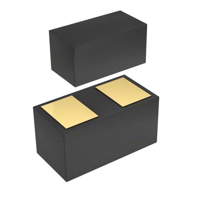
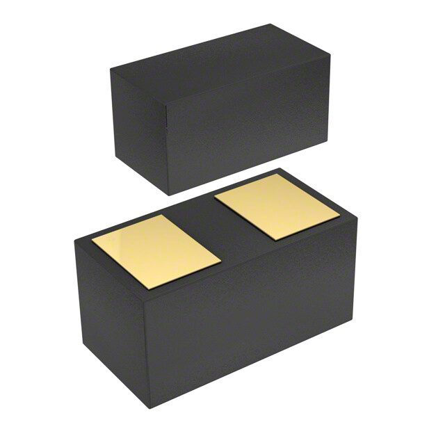
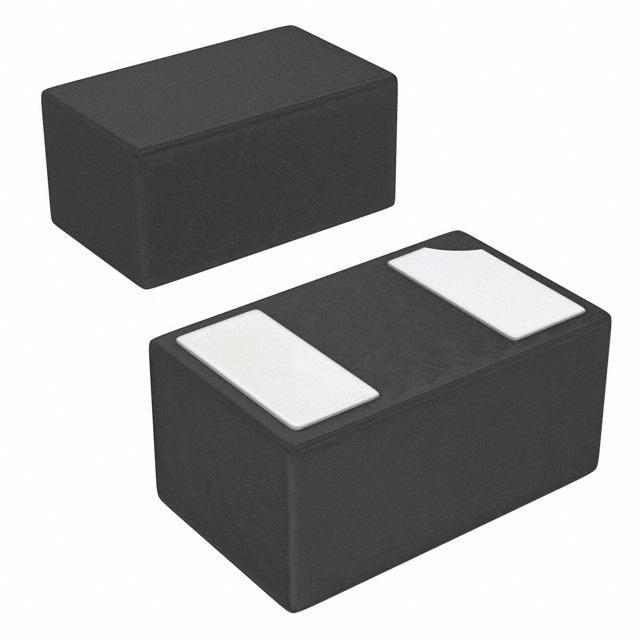
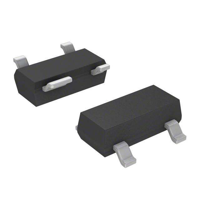
| 描述 | TVS DIODE 5.5VWM 13VC WLL2-1 |
| 产品分类 | |
| 品牌 | Infineon Technologies |
| 数据手册 | http://www.infineon.com/dgdl/ESD200-B1-CSP0201.pdf?folderId=db3a30431f848401011fcbf2ab4c04c4&fileId=db3a30433ee50ba8013eea92ca691505 |
| 产品图片 |
|
| 产品型号 | ESD200B1CSP0201XTSA1 |
| rohs | 无铅 / 符合限制有害物质指令(RoHS)规范要求 |
| 产品系列 | - |
| 不同频率时的电容 | 6.5pF @ 1MHz |
| 产品培训模块 | http://www.digikey.cn/PTM/IndividualPTM.page?site=cn&lang=zhs&ptm=30476 |
| 供应商器件封装 | - |
| 其它名称 | ESD200B1CSP0201XTSA1CT |
| 功率-峰值脉冲 | - |
| 包装 | 剪切带 (CT) |
| 单向通道 | - |
| 双向通道 | 1 |
| 安装类型 | 表面贴装 |
| 封装/外壳 | 2-SMD |
| 工作温度 | -40°C ~ 125°C |
| 应用 | 通用 |
| 标准包装 | 1 |
| 电压-击穿(最小值) | 6V |
| 电压-反向关态(典型值) | 5.5V(最小值) |
| 电压-箝位(最大值)@Ipp | 13V (标准) |
| 电流-峰值脉冲(10/1000µs) | 16A (8/20µs) |
| 电源线路保护 | 无 |
| 类型 | 齐纳 |


- 商务部:美国ITC正式对集成电路等产品启动337调查
- 曝三星4nm工艺存在良率问题 高通将骁龙8 Gen1或转产台积电
- 太阳诱电将投资9.5亿元在常州建新厂生产MLCC 预计2023年完工
- 英特尔发布欧洲新工厂建设计划 深化IDM 2.0 战略
- 台积电先进制程称霸业界 有大客户加持明年业绩稳了
- 达到5530亿美元!SIA预计今年全球半导体销售额将创下新高
- 英特尔拟将自动驾驶子公司Mobileye上市 估值或超500亿美元
- 三星加码芯片和SET,合并消费电子和移动部门,撤换高东真等 CEO
- 三星电子宣布重大人事变动 还合并消费电子和移动部门
- 海关总署:前11个月进口集成电路产品价值2.52万亿元 增长14.8%


PDF Datasheet 数据手册内容提取
TVS Diode Transient Voltage Suppressor Diodes ESD200-B1-CSP0201 Low Clamping Voltage TVS Diode in a Thin 0201 Chip Scale Package ESD200-B1-CSP0201 Data Sheet Revision 1.0, 2013-05-21 Final Power Management & Multimarket
Edition 2013-05-21 Published by Infineon Technologies AG 81726 Munich, Germany © 2013 Infineon Technologies AG All Rights Reserved. Legal Disclaimer The information given in this document shall in no event be regarded as a guarantee of conditions or characteristics. With respect to any examples or hints given herein, any typical values stated herein and/or any information regarding the application of the device, Infineon Technologies hereby disclaims any and all warranties and liabilities of any kind, including without limitation, warranties of non-infringement of intellectual property rights of any third party. Information For further information on technology, delivery terms and conditions and prices, please contact the nearest Infineon Technologies Office (www.infineon.com). Warnings Due to technical requirements, components may contain dangerous substances. For information on the types in question, please contact the nearest Infineon Technologies Office. Infineon Technologies components may be used in life-support devices or systems only with the express written approval of Infineon Technologies, if a failure of such components can reasonably be expected to cause the failure of that life-support device or system or to affect the safety or effectiveness of that device or system. Life support devices or systems are intended to be implanted in the human body or to support and/or maintain and sustain and/or protect human life. If they fail, it is reasonable to assume that the health of the user or other persons may be endangered.
ESD200-B1-CSP0201 Revision History: Revision 0.9.3, 2012-03.13 Page or Item Subjects (major changes since previous revision) Revision 1.0, 2013-05-21 All Status change to final Trademarks of Infineon Technologies AG AURIX™, BlueMoon™, C166™, CanPAK™, CIPOS™, CIPURSE™, COMNEON™, EconoPACK™, CoolMOS™, CoolSET™, CORECONTROL™, CROSSAVE™, DAVE™, EasyPIM™, EconoBRIDGE™, EconoDUAL™, EconoPIM™, EiceDRIVER™, eupec™, FCOS™, HITFET™, HybridPACK™, I²RF™, ISOFACE™, IsoPACK™, MIPAQ™, ModSTACK™, my-d™, NovalithIC™, OmniTune™, OptiMOS™, ORIGA™, PRIMARION™, PrimePACK™, PrimeSTACK™, PRO-SIL™, PROFET™, RASIC™, ReverSave™, SatRIC™, SIEGET™, SINDRION™, SIPMOS™, SMARTi™, SmartLEWIS™, SOLIDFLASH™, TEMPFET™, thinQ!™, TRENCHSTOP™, TriCore™, X-GOLD™, X-PMU™, XMM™, XPOSYS™. Other Trademarks Advance Design System™ (ADS) of Agilent Technologies, AMBA™, ARM™, MULTI-ICE™, KEIL™, PRIMECELL™, REALVIEW™, THUMB™, µVision™ of ARM Limited, UK. AUTOSAR™ is licensed by AUTOSAR development partnership. Bluetooth™ of Bluetooth SIG Inc. CAT-iq™ of DECT Forum. COLOSSUS™, FirstGPS™ of Trimble Navigation Ltd. EMV™ of EMVCo, LLC (Visa Holdings Inc.). EPCOS™ of Epcos AG. FLEXGO™ of Microsoft Corporation. FlexRay™ is licensed by FlexRay Consortium. HYPERTERMINAL™ of Hilgraeve Incorporated. IEC™ of Commission Electrotechnique Internationale. IrDA™ of Infrared Data Association Corporation. ISO™ of INTERNATIONAL ORGANIZATION FOR STANDARDIZATION. MATLAB™ of MathWorks, Inc. MAXIM™ of Maxim Integrated Products, Inc. MICROTEC™, NUCLEUS™ of Mentor Graphics Corporation. Mifare™ of NXP. MIPI™ of MIPI Alliance, Inc. MIPS™ of MIPS Technologies, Inc., USA. muRata™ of MURATA MANUFACTURING CO., MICROWAVE OFFICE™ (MWO) of Applied Wave Research Inc., OmniVision™ of OmniVision Technologies, Inc. Openwave™ Openwave Systems Inc. RED HAT™ Red Hat, Inc. RFMD™ RF Micro Devices, Inc. SIRIUS™ of Sirius Satellite Radio Inc. SOLARIS™ of Sun Microsystems, Inc. SPANSION™ of Spansion LLC Ltd. Symbian™ of Symbian Software Limited. TAIYOYUDEN™ of Taiyo Yuden Co. TEAKLITE™ of CEVA, Inc. TEKTRONIX™ of Tektronix Inc. TOKO™ of TOKO KABUSHIKI KAISHA TA. UNIX™ of X/Open Company Limited. VERILOG™, PALLADIUM™ of Cadence Design Systems, Inc. VLYNQ™ of Texas Instruments Incorporated. VXWORKS™, WIND RIVER™ of WIND RIVER SYSTEMS, INC. ZETEX™ of Diodes Zetex Limited. Last Trademarks Update 2010-10-26 Final Data Sheet 3 Revision 1.0, 2013-05-21
ESD200-B1-CSP0201 Low Clamping Voltage TVS Diode in a Thin 0201 Chip Scale Package 1 Low Clamping Voltage TVS Diode in a Thin 0201 Chip Scale Package 1.1 Features • ESD / Transient protection of susceptible I/O lines to: – IEC61000-4-2 (ESD): ±16kV (air/contact discharge) – IEC61000-4-5 (surge): ±3A (8/20μs)) • Low clamping voltage • Low dynamic resistance: R ≤0.2Ω typ. DYN • Supports applications with signal voltage between -5.5V and 5.5V max. • Line capacitance: C =6.5pF L • Minimized overshoot due to extremely low parasitic inductance of chip scale package • Miniature form factor (XY) = 0201 (0.58mmx0.28mm) • Thin 0.15mm package thickness to allow direct integration into modules • Optimized assembly: its bidirectional and symmetric I/V characteristics allow placement on the PCB with no danger of polarity orientation issues 1.2 Application Examples • ESD Protection of highly susceptible IC/ASICs in audio, headset, human digital interfaces • Dedicated solution to boost space saving and high performance in miniaturized modern electronics 1.3 Product Description a) Pin configuration top view b) Schematic diagram Configuration_Schematic_Diagram.vst.vsd Figure1-1 Pin Configuration and Schematic Diagram Table1-1 Ordering Information Type Package Configuration Marking code ESD200-B1-CSP0201 WLL-2-1 1 line, bi-directional A1) 1) The device does not have any marking or date code on the device backside. The Marking code is on pad side. Final Data Sheet 4 Revision 1.0, 2013-05-21
ESD200-B1-CSP0201 Characteristics 2 Characteristics 2.1 Maximum Ratings Table2-1 Maximum Ratings at T = 25°C, unless otherwise specified A Parameter Symbol Values Unit Min. Typ. Max. ESD1) V kV ESD Contact discharge -16 - 16 Air discharge -16 - 16 Peak pulse current (t = 8/20μs)2) I -3 - 3 A p PP Operating temperature range T -40 - 125 °C OP Storage temperature T -65 - 150 °C stg 1) V according to IEC61000-4-2 (R = 330, C = 150 pF discharge network) ESD 2) I according to IEC61000-4-5 (t = 8/20 μs) PP p Attention:Stresses above the max. values listed here may cause permanent damage to the device. Exposure to absolute maximum rating conditions for extended periods may affect device reliability. Maximum ratings are absolute ratings; exceeding only one of these values may cause irreversible damage to the integrated circuit. 2.2 Electrical Characteristics at T = 25 °C, unless otherwise specified A (cid:9)(cid:3) (cid:9) (cid:12)(cid:12) (cid:9) (cid:10)(cid:11)(cid:12) (cid:2)(cid:3) (cid:17)(cid:17)(cid:17) (cid:2)(cid:3)(cid:4)(cid:5)(cid:6)(cid:4)(cid:7)(cid:8)(cid:9)(cid:3)(cid:10)(cid:11)(cid:6)(cid:12)(cid:13) (cid:9)(cid:3) (cid:17)(cid:17)(cid:17) (cid:2)(cid:3)(cid:4)(cid:5)(cid:6)(cid:4)(cid:7)(cid:8)(cid:16)(cid:17)(cid:4)(cid:4)(cid:13)(cid:18)(cid:11) (cid:8)(cid:2) (cid:2)(cid:4) (cid:17)(cid:17)(cid:17) (cid:14)(cid:13)(cid:9)(cid:13)(cid:4)(cid:15)(cid:13)(cid:8)(cid:9)(cid:3)(cid:10)(cid:11)(cid:6)(cid:12)(cid:13) (cid:4) (cid:9)(cid:4) (cid:17)(cid:17)(cid:17) (cid:14)(cid:13)(cid:9)(cid:13)(cid:4)(cid:15)(cid:13)(cid:8)(cid:16)(cid:17)(cid:4)(cid:4)(cid:13)(cid:18)(cid:11) (cid:5)(cid:6)(cid:7) (cid:8)(cid:9) (cid:8)(cid:9) (cid:8)(cid:2) (cid:2) (cid:4)(cid:16) (cid:9) (cid:4) (cid:2) (cid:2) (cid:2) (cid:10)(cid:11)(cid:12) (cid:15)(cid:4) (cid:4)(cid:13)(cid:14) (cid:9) (cid:2)(cid:4) (cid:4)(cid:13)(cid:14) (cid:2)(cid:3) (cid:9)(cid:4)(cid:13)(cid:14) (cid:2)(cid:4)(cid:13)(cid:14)(cid:2)(cid:15)(cid:4) (cid:2)(cid:3)(cid:16) (cid:9) (cid:2) (cid:4) (cid:10)(cid:11)(cid:12) (cid:8)(cid:2) (cid:4)(cid:5)(cid:6)(cid:7) (cid:17)(cid:17)(cid:17) (cid:19)(cid:27)(cid:18)(cid:6)(cid:28)(cid:20)(cid:16)(cid:8)(cid:4)(cid:13)(cid:15)(cid:20)(cid:15)(cid:11)(cid:6)(cid:18)(cid:16)(cid:13) (cid:8)(cid:2) (cid:2)(cid:4)(cid:13)(cid:14)(cid:17)(cid:17)(cid:17) (cid:14)(cid:13)(cid:9)(cid:13)(cid:4)(cid:15)(cid:13)(cid:8)(cid:5)(cid:3)(cid:4)(cid:30)(cid:20)(cid:18)(cid:12)(cid:8)(cid:9)(cid:3)(cid:10)(cid:11)(cid:6)(cid:12)(cid:13)(cid:8)(cid:28)(cid:6)(cid:31)(cid:26) (cid:8)(cid:9) (cid:4)(cid:5)(cid:6)(cid:7) (cid:8)(cid:9) (cid:2)(cid:15)(cid:4) (cid:17)(cid:17)(cid:17) (cid:24)(cid:4)(cid:13)(cid:6)(cid:30)(cid:7)(cid:3)(cid:5)(cid:18)(cid:8)(cid:9)(cid:3)(cid:10)(cid:11)(cid:6)(cid:12)(cid:13) (cid:2)(cid:3)(cid:16) (cid:17)(cid:17)(cid:17) (cid:2)(cid:3)(cid:4)(cid:5)(cid:6)(cid:4)(cid:7)(cid:8)(cid:16)(cid:10)(cid:6)(cid:28)(cid:29)(cid:20)(cid:18)(cid:12)(cid:8)(cid:9)(cid:3)(cid:10)(cid:11)(cid:6)(cid:12)(cid:13) (cid:2)(cid:4)(cid:16) (cid:17)(cid:17)(cid:17) (cid:14)(cid:13)(cid:9)(cid:13)(cid:4)(cid:15)(cid:13)(cid:8)(cid:16)(cid:10)(cid:6)(cid:28)(cid:29)(cid:20)(cid:18)(cid:12)(cid:8)(cid:9)(cid:3)(cid:10)(cid:11)(cid:6)(cid:12)(cid:13) (cid:2)(cid:10)(cid:11)(cid:12) (cid:17)(cid:17)(cid:17) !"(cid:8)(cid:9)(cid:3)(cid:10)(cid:11)(cid:6)(cid:12)(cid:13) (cid:9)(cid:4)(cid:13)(cid:14) (cid:17)(cid:17)(cid:17) (cid:14)(cid:13)(cid:9)(cid:13)(cid:4)(cid:15)(cid:13)(cid:8)(cid:5)(cid:3)(cid:4)(cid:30)(cid:20)(cid:18)(cid:12)(cid:8)(cid:16)(cid:17)(cid:4)(cid:4)(cid:13)(cid:18)(cid:11)(cid:8)(cid:28)(cid:6)(cid:31)(cid:26) (cid:9)(cid:12)(cid:12) (cid:9)(cid:4) (cid:17)(cid:17)(cid:17) (cid:14)(cid:13)(cid:9)(cid:13)(cid:4)(cid:15)(cid:13)(cid:8)(cid:16)(cid:17)(cid:4)(cid:4)(cid:13)(cid:18)(cid:11) (cid:9) (cid:9)(cid:12)(cid:12) (cid:17)(cid:17)(cid:17) "(cid:13)(cid:6)(cid:30)(cid:8)(cid:29)(cid:17)(cid:10)(cid:15)(cid:13)(cid:8)(cid:16)(cid:17)(cid:4)(cid:4)(cid:13)(cid:18)(cid:11) (cid:10)(cid:11)(cid:12) (cid:9)(cid:10)(cid:11)(cid:12) (cid:17)(cid:17)(cid:17) !"(cid:8)(cid:16)(cid:17)(cid:4)(cid:4)(cid:13)(cid:18)(cid:11) (cid:9)(cid:4) (cid:19)(cid:20)(cid:3)(cid:7)(cid:13)(cid:21)(cid:22)(cid:23)(cid:6)(cid:4)(cid:6)(cid:16)(cid:11)(cid:13)(cid:4)(cid:20)(cid:15)(cid:11)(cid:20)(cid:16)(cid:21)(cid:22)(cid:17)(cid:4)(cid:9)(cid:13)(cid:21)(cid:24)(cid:20)(cid:25)(cid:7)(cid:20)(cid:4)(cid:13)(cid:16)(cid:11)(cid:20)(cid:3)(cid:18)(cid:6)(cid:10)(cid:26)(cid:15)(cid:9)(cid:12) Figure2-1 Definitions of electrical characteristics Final Data Sheet 5 Revision 1.0, 2013-05-21
ESD200-B1-CSP0201 Characteristics Table2-2 DC Characteristics at T = 25°C, unless otherwise specified A Parameter Symbol Values Unit Note / TestCondition Min. Typ. Max. Reverse working voltage V -5.5 - 5.5 V RWM Breakdown voltage V 6 - 10 V I =1mA BR BR Reverse current I - 0.1 100 nA V =5.5V R R Table2-3 RF Characteristics at T = 25°C, unless otherwise specified A Parameter Symbol Values Unit Note / TestCondition Min. Typ. Max. Line capacitance C 6.5 pF V =0V, f =1MHz L R Table2-4 ESD Characteristics at T = 25°C, unless otherwise specified A Parameter Symbol Values Unit Note / TestCondition Min. Typ. Max. Clamping voltage1) V - 12 - V V =8kV CL ESD contact discharge Clamping voltage2) - 10 - I =1A TLP - 13 - I =16A TLP Clamping voltage3) - 10 - I =1A PP - 12.5 - I =3A PP Dynamic resistance2) R - 0.2 - Ω DYN 1) V according to IEC61000-4-2 (R=330Ω, C=150pF discharge network) ESD 2) ANSI/ESDSTM5.5.1-Electrostatistic Discharge Sensitivity Testing using Transmission Line Pulse (TLP) Model. TLP conditions: Z =50Ω, t =100ns, t =0.6ns, I and V average window: t =30ns to t =60ns, extraction of dynamic 0 p r TLP TLP 1 2 resistance using squares fit to TLP characteristics between I =2.5A and I =17A. Please refer to Application Note TLP1 TLP2 AN210[1] 3) I according to IEC61000-4-5 (t =8/20μs) PP p Final Data Sheet 6 Revision 1.0, 2013-05-21
ESD200-B1-CSP0201 Typical Characteristics 3 Typical Characteristics Curves specified at T =25°C, unless otherwise specified A -3 10 -4 10 -5 10 -6 10 -7 10 ] A [ R 10-8 I -9 10 -10 10 -11 10 -12 10 -10 -8 -6 -4 -2 0 2 4 6 8 10 V [V] R Figure3-1 Reverse current: I =f(V ) R R +1 10 ] A +0 n 10 [ R I -1 10 -40 -30 -20 -10 0 10 20 30 40 50 60 70 80 90 100 110 120 130 T [°C] A Figure3-2 Reverse current: I =f(T ), V =5.5V R A R Final Data Sheet 7 Revision 1.0, 2013-05-21
ESD200-B1-CSP0201 Typical Characteristics 9 8.9 8.8 8.7 8.6 ] V [ 8.5 R B V 8.4 8.3 8.2 8.1 8 -40 -30 -20 -10 0 10 20 30 40 50 60 70 80 90 100 110 120 130 T [°C] A Figure3-3 Reverse voltage: V =f(T ), I =1mA BR A R 10 9 8 7 6 ] F p 5 [ L C 4 3 2 1 0 -3 -2.5 -2 -1.5 -1 -0.5 0 0.5 1 1.5 2 2.5 3 V [V] R Figure3-4 Line capacitance: C =f(V ), f=1MHz L R Final Data Sheet 8 Revision 1.0, 2013-05-21
ESD200-B1-CSP0201 Typical Characteristics 30 15 ESD200-B1-CSP0201 R DYN 25 12.5 20 10 15 7.5 R = 0.20 Ω DYN 10 5 ] 5 2.5 V k [ C ] E A VI [ 0 0 P t L n T e I al v -5 -2.5 ui q E -10 -5 R = 0.20 Ω DYN -15 -7.5 -20 -10 -25 -12.5 -30 -15 -20 -15 -10 -5 0 5 10 15 20 V [V] TLP Figure3-5 Clamping voltage (TLP): I =f(V ) according ANSI/ESDSTM5.5.1-Electrostatistic TLP TLP Discharge Sensitivity Testing using Transmission Line Pulse (TLP) Model. TLP conditions: Z =50Ω, t =100ns, t =0.6ns, I and V average window: t =30ns to t =60ns, 0 p r TLP TLP 1 2 extraction of dynamic resistance using squares fit to TLP characteristics between I =2.5A and I =17A. Please refer to Application Note AN210[1] TLP1 TLP2 Final Data Sheet 9 Revision 1.0, 2013-05-21
ESD200-B1-CSP0201 Typical Characteristics 5 ESD200-B1-CSP0201 R DYN 4 3 R = 1 Ω DYN 2 1 ] A [ 0 P P I -1 -2 R = 1 Ω DYN -3 -4 -5 -20 -15 -10 -5 0 5 10 15 20 V [V] CL Figure3-6 Pulse current (IEC61000-4-5) versus clamping voltage: I =f(V ) PP CL Final Data Sheet 10 Revision 1.0, 2013-05-21
ESD200-B1-CSP0201 Typical Characteristics 50 Scope: 6 GHz, 20 GS/s 45 40 V = 25 V 35 CL-max-peak V = 12 V 30 CL-30ns-peak V] 25 [ L C 20 V 15 10 5 0 -5 -100 0 100 200 300 400 500 600 700 800 900 t [ns] p Figure3-7 IEC61000-4-2: V =f(t), +8kV pulse CL 5 0 -5 -10 -15 V] -20 [ L C -25 V -30 V = -24 V CL-max-peak -35 V = -11 V CL-30ns-peak -40 -45 Scope: 6 GHz, 20 GS/s -50 -100 0 100 200 300 400 500 600 700 800 900 t [ns] p Figure3-8 IEC61000-4-2: V =f(t), -8kV pulse CL Final Data Sheet 11 Revision 1.0, 2013-05-21
ESD200-B1-CSP0201 Typical Characteristics 50 Scope: 6 GHz, 20 GS/s 45 40 V = 34 V 35 CL-max-peak V = 13 V 30 CL-30ns-peak V] 25 [ L C 20 V 15 10 5 0 -5 -100 0 100 200 300 400 500 600 700 800 900 t [ns] p Figure3-9 IEC61000-4-2: V =f(t), +15kV pulse CL 5 0 -5 -10 -15 V] -20 [ L C -25 V -30 V = -35 V CL-max-peak -35 V = -12 V CL-30ns-peak -40 -45 Scope: 6 GHz, 20 GS/s -50 -100 0 100 200 300 400 500 600 700 800 900 t [ns] p Figure3-10 IEC61000-4-2: V =f(t), -15kV pulse CL Final Data Sheet 12 Revision 1.0, 2013-05-21
ESD200-B1-CSP0201 Application Information 4 Application Information Protected data line with signal level r cto -5.5 V up to +5.5 V (bi-directional) ESD ne I/O sensitive n o device C 1 The protection diode should be placed very close to the location where the ESD or other transients can occur to keep loops and inductances as small as possible . Pin 2(or pin 1) should be connected directly to a ground plane on the board. 2 Application_ESD200-B1-CSP0201.vsd Figure4-1 Single line, bi-directional ESD / Transient protection Final Data Sheet 13 Revision 1.0, 2013-05-21
ESD200-B1-CSP0201 Package 5 Package Figure5-1 WLL-2-1 Package outline (dimension in mm) 0.32 0.24 0.27 0.19 4 1 0. 2 7 6 5 0. 0. 9 1 9 0. 0.24 0.1 Copper Solder mask Stencil apertures Figure5-2 WLL-2-1 Footprint (dimension in mm) 0.23 8 6 0. 8 2 0.21 0.35 Deliveries can be in Embossed Tape with or without vacuum hole (no selection possible). Specification allows identical processing (pick & place) by users. SG-WLL-2-1-TP V02 Figure5-3 WLL-2-1 Packing (dimension in mm) Marking on pad-side Type code SG-WLL-2-1-MK V01 Figure5-4 WLL-2-1 Marking (example) Final Data Sheet 14 Revision 1.0, 2013-05-21
ESD200-B1-CSP0201 References References [1] Infineon AG - Application Note AN210: Effective ESD Protection design at System Level Using VF-TLP Characterization Methodology Final Data Sheet 15 Revision 1.0, 2013-05-21
w w w . i n f i n e o n . c o m Published by Infineon Technologies AG
Mouser Electronics Authorized Distributor Click to View Pricing, Inventory, Delivery & Lifecycle Information: I nfineon: ESD200B1CSP0201XTSA1