 Datasheet下载
- 型号: SR05-02CTG
- 制造商: Littelfuse
- 库位|库存: xxxx|xxxx
- 要求:
| 数量阶梯 | 香港交货 | 国内含税 |
| +xxxx | $xxxx | ¥xxxx |
查看当月历史价格
查看今年历史价格
SR05-02CTG产品简介:
ICGOO电子元器件商城为您提供SR05-02CTG由Littelfuse设计生产,在icgoo商城现货销售,并且可以通过原厂、代理商等渠道进行代购。 SR05-02CTG价格参考。LittelfuseSR05-02CTG封装/规格:TVS - 二极管, 。您可以下载SR05-02CTG参考资料、Datasheet数据手册功能说明书,资料中有SR05-02CTG 详细功能的应用电路图电压和使用方法及教程。
Littelfuse Inc.生产的SR05-02CTG是一款瞬态电压抑制(TVS)二极管,主要用于保护电子电路免受瞬态电压的损害。以下是该型号的应用场景:

1. 电源线保护:SR05-02CTG可以用于交流或直流电源输入端口,防止因雷击、开关噪声或其他瞬态事件引起的过电压对设备造成损坏。

2. 信号线路保护:适用于各种信号线路,如RS-232、USB、以太网等接口,提供静电放电(ESD)和浪涌保护,确保数据传输的稳定性。

3. 汽车电子系统:在汽车环境中,这款TVS二极管可用于保护车载电子系统,例如CAN总线、LIN总线以及传感器线路,抵御负载突降和感应浪涌。

4. 通信设备:在电信设备中,用于保护天线接口、射频模块和其他敏感组件,避免由外部干扰或内部故障引发的过压问题。

5. 工业控制:为工业自动化设备中的I/O端口、继电器触点及传感器连接提供可靠的防护,延长设备使用寿命。

6. 消费类电子产品:广泛应用于电视、音响、家用电器等产品中,保障其内部电路在面对意外电压波动时的安全性。

7. 医疗设备:在需要高可靠性的医疗仪器中,用作关键部件的保护措施,确保设备运行的精确性和安全性。

总之,SR05-02CTG凭借其快速响应时间、高能量吸收能力和低漏电流特性,成为众多领域中理想的过电压保护解决方案。
| 参数 | 数值 |
| 产品目录 | |
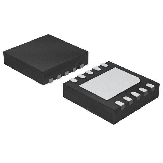
| 描述 | TVS DIODE 5VWM 18VC SOT143TVS二极管阵列 2CH 25A 5V 6pF Lightning Protection |
| 产品分类 | |
| 品牌 | Littelfuse |
| 产品手册 | |
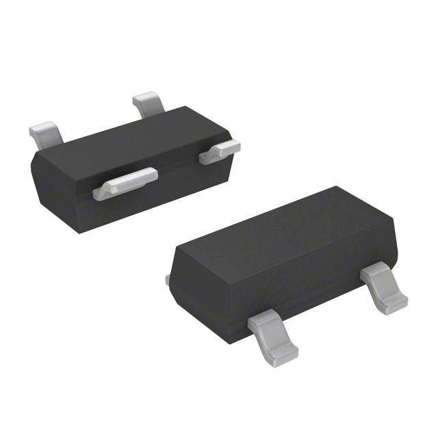
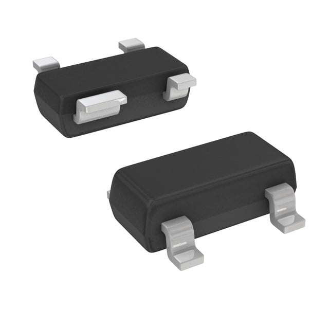
| 产品图片 |
|
| rohs | 符合RoHS无铅 / 符合限制有害物质指令(RoHS)规范要求 |
| 产品系列 | 二极管与整流器,TVS二极管,TVS二极管阵列,Littelfuse SR05-02CTGSR05, SPA® |
| 数据手册 | |
| 产品型号 | SR05-02CTG |
| 不同频率时的电容 | - |
| 产品培训模块 | http://www.digikey.cn/PTM/IndividualPTM.page?site=cn&lang=zhs&ptm=25590 |
| 产品种类 | TVS二极管阵列 |
| 供应商器件封装 | SOT-143 |
| 其它名称 | F6188CT |
| 击穿电压 | 6 V |
| 功率-峰值脉冲 | 450W |
| 包装 | 剪切带 (CT) |
| 单向通道 | - |
| 双向通道 | 2 |
| 商标 | Littelfuse |
| 外壳高度 | 1.22 mm |
| 安装类型 | 表面贴装 |
| 安装风格 | SMD/SMT |
| 封装 | Reel |
| 封装/外壳 | SOT-143R |
| 封装/箱体 | SOT-143 |
| 峰值浪涌电流 | 25 A |
| 峰值脉冲功率耗散 | 450 W |
| 工作温度 | -40°C ~ 125°C (TJ) |
| 工作电压 | 5 V |
| 工厂包装数量 | 3000 |
| 应用 | 以太网 |
| 最大工作温度 | + 125 C |
| 最小工作温度 | - 40 C |
| 标准包装 | 1 |
| 特色产品 | http://www.digikey.cn/product-highlights/zh/sr05-series-tvs-diodes-array-high-speed/52863 |
| 电压-击穿(最小值) | 6V |
| 电压-反向关态(典型值) | 5V(最小值) |
| 电压-箝位(最大值)@Ipp | 18V |
| 电容 | 3 pF, 6 pF |
| 电流-峰值脉冲(10/1000µs) | 25A (8/20µs) |
| 电源线路保护 | 是 |
| 端接类型 | SMD/SMT |
| 类型 | 转向装置(轨至轨) |
| 系列 | SR05 |
| 通道 | 2 Channels |
| 钳位电压 | 9.8 V, 12 V, 18 V |


- 商务部:美国ITC正式对集成电路等产品启动337调查
- 曝三星4nm工艺存在良率问题 高通将骁龙8 Gen1或转产台积电
- 太阳诱电将投资9.5亿元在常州建新厂生产MLCC 预计2023年完工
- 英特尔发布欧洲新工厂建设计划 深化IDM 2.0 战略
- 台积电先进制程称霸业界 有大客户加持明年业绩稳了
- 达到5530亿美元!SIA预计今年全球半导体销售额将创下新高
- 英特尔拟将自动驾驶子公司Mobileye上市 估值或超500亿美元
- 三星加码芯片和SET,合并消费电子和移动部门,撤换高东真等 CEO
- 三星电子宣布重大人事变动 还合并消费电子和移动部门
- 海关总署:前11个月进口集成电路产品价值2.52万亿元 增长14.8%


PDF Datasheet 数据手册内容提取
TVS Diode Arrays (SPA® Diodes) Lightning Surge Protection- SR05 Series SR05 Series 5V 25A Diode Array RoHS Pb GREEN Description The SR05 consists of four, low capacitance steering diodes and a low voltage TVS diode that provide protection against ESD and lightning surge events. Each channel or I/O pin can safely absorb up to 25A (tp=8/20μs) and repetitive ESD strikes above the maximum level (Level 4) specified in the IEC 61000-4-2 international standard without performance degradation. The low loading capacitance makes it ideal for protecting high-speed telecommunication data lines. Pinout SOT143 Features • ESD, IEC61000-4-2 , • Low capacitance of 6.0pF ±30kV contact discharge, (TYP) per I/O ±30kV air discharge • Low clamp voltage Vcc GND • EFT, IEC61000-4-4, 80A • Small SOT143 (JEDEC TO- (tp=5/50ns) 253) packaging • Lightning protection, • Moisture Sensitivity Level IEC61000-4-5, 25A (MSL-1) (t =8/20µs) p I/O 1 I/O 2 Applications Functional Block Diagram • T1/E1 IC/Secondary • ISDN S/T Interface PIN 4 Protection • Video Lines • Ethernet 10BaseT • Microcontroller Input • WAN/LAN Equipment Protection PIN 2 PIN 3 Application Example I/O I/O V CC GND (PIN 1) 1 4 Additional Information 2 3 Datasheet Resources Samples The SR05 integrates a TVS Diode between the Vcc and Gnd pins. This allows the array to protect the power supply Life Support Note: against ESD and lighting surges when these pins are both Not Intended for Use in Life Support or Life Saving Applications connected in the application. The products shown herein are not designed for use in life sustaining or life saving applications unless otherwise expressly indicated. © 2017 Littelfuse, Inc. Specifications are subject to change without notice. Revised: 02/23/17
TVS Diode Arrays (SPA® Diodes) Lightning Surge Protection- SR05 Series Absolute Maximum Ratings Thermal Information Symbol Parameter Value Units Parameter Rating Units I Peak Current (t=8/20μs) 25.0 A Storage Temperature Range –55 to 150 °C PP p P Peak Pulse Power (t=8/20μs) 450 W Maximum Junction Temperature 150 °C Pk p Maximum Lead Temperature 260 °C T Operating Temperature –40 to 125 °C OP (Soldering 20-40s) T Storage Temperature –55 to 150 °C STOR CAUTION: Stresses above those listed in “Absolute Maximum Ratings” may cause permanent damage to the device. This is a stress only rating and operation of the device at these or any other conditions above those indicated in the operational sections of this specification is not implied. Electrical Characteristics (T =25ºC) OP Parameter Symbol Test Conditions Min Typ Max Units Reverse Stand-Off Voltage V - - 5.0 V RWM Reverse Leakage Current I V = 5V, I/O to GND - - 5.0 µA R R Reverse Breakdown Voltage V I = 1mA 6.0 - - V BR t Clamping Voltage, Line-Ground1 V I = 1A, t=8/20 µs - - 9.8 V C PP p Clamping Voltage, Line-Ground1 V I = 10A, t=8/20 µs - - 12.0 V C PP p Clamping Voltage, Line-Ground1 V I = 25A, t=8/20 µs - - 18.0 V C PP p Dynamic Resistance, Line-Ground1 R ( V -V )/(I -I ) - 0.3 - W DYN C2 C1 PP2 PP1 IEC61000-4-2 (Contact Discharge) ±30 - - kV ESD Withstand Voltage1 V ESD IEC61000-4-2 (Air Discharge) ±30 kV C Reverse Bias=0V - 3.0 - pF I/O-I/O Diode Capacitance1 C Reverse Bias=0V - 6.0 10.0 pF I/O-GND Note: 1. Parameter is guaranteed by design and/or device characterization. Capacitance vs. Reverse Bias 8/20μs Pulse Waveform 10.0 110% 9.0 100% 8.0 90% acitance (pF) 567...000 Vcc Open nt of IPP 56780000%%%% p e Ca 4.0 erc 40% 3.0 Vcc=3.3V Vcc=5V P 30% 2.0 20% 10% 1.0 0% 0.0 0.0 5.0 10.0 15.0 20.0 25.0 30.0 0.0 1.0 2.0 3.0 4.0 5.0 Time (μs) Reverse Bias (V) © 2017 Littelfuse, Inc. Specifications are subject to change without notice. Revised: 02/23/17
TVS Diode Arrays (SPA® Diodes) Lightning Surge Protection- SR05 Series Clamping Voltage vs. I Product Characteristics PP Lead Plating Matte Tin Lead Material Copper Alloy 20 Lead Coplanarity 0.0004 inches (0.102mm) Substitute Material Silicon V)C15 Body Material Molded Epoxy e ( ag Flammability UL 94 V-0 mp Volt 10 N1. o Atells d :i mensions are in millimeters Cla 23.. DDiimmeennssiioonnss ianrcel uedxec lusosilvdee ro pf lmatoinldg .flash & metal burr. 5 4. Blo is facing up for mold and facing down for trim/form, i.e. reverse trim/form. 5. Package surface matte finish VDI 11-13. 0 0 5 10 15 20 25 Peak Pulse Current-I (A) PP Soldering Parameters Reflow Condition Pb – Free assembly tP TP CCrriittiiccaall ZZoonnee - Temperature Min (Ts(min)) 150°C e RRaammpp--uupp TTLL ttoo TTPP Pre Heat -- TTeimmep e(mraitnu rteo Mmaaxx )( T(ts()max)) 2600 0–° C180 secs rutare TS(mTaxL) tL s pm RRaammpp--ddoown Average ramp up rate (Liquidus) Temp e PPrreehheeaatt 3°C/second max T (TL) to peak TS(min) tS T to T - Ramp-up Rate 3°C/second max S(max) L Reflow -- TTeemmppeerraattuurree ((TtL)) (Liquidus) 26107 –° C1 50 seconds 25 time to peak temperature Time L Peak Temperature (T ) 260+0/-5 °C P Time within 5°C of actual peak 20 – 40 seconds Temperature (t ) Ordering Information p Ramp-down Rate 6°C/second max Time 25°C to peak Temperature (T ) 8 minutes Max. Part Number Package Marking Min. Order Qty. P Do not exceed 260°C SR05-02CTG SOT143 SR05 3000 Part Numbering System Part Marking System SR 05 –02 C T G G= Green T= Tape & Reel SR05 Series Number of Package Channels C: SOT143 © 2017 Littelfuse, Inc. Specifications are subject to change without notice. Revised: 02/23/17
TVS Diode Arrays (SPA® Diodes) Lightning Surge Protection- SR05 Series Package Dimensions—SOT143 Package SOT143 e Pins 4 e 4 3 JEDEC TO-253 Recommended Pad Layout Millimeters Inches 4 3 503B 0.80 (.032") E1 E 1.00 (.040") Min Max Min Max 503B E1 E 1 2 01..8000 ((..003420"")) AA1 1.40 (.M05A5X"0)0..085 01..2125 00.0.0032 00..004086 3.40 (.134") 2.20 1.90 e1 3.60 (.11.4400" )(.0(.5R058E7"F)") (.10.77b50" ) 0.30 0.50 0.012 0.020 1 2 MAX (.0b672") 0.76 0.89 0.030 0.035 e1 D 33..4600 ((..113440"")) (.20.8270" ) (.10.7950" ) BScC 0.08 0.20 0.003 0.008 REF 1.70 D 2.80 3.04 0.110 0.120 A (.067") D BSC 11..0200 ((..004408""))E01..8000 ((..003420"")) 2.10 2.64 0.082 0.104 E1 1.20 1.40 0.047 0.055 b2 b A1 A e 1.92 BSC 0.076 BSC 1.00 (.040") 0.80 (.032") 1.20 (.048") 1.00 (.040") e1 0.20 BSC 0.008 BSC c L 0.4 0.6 0.016 0.024 b2 b A1 L L1 0.550 REF 0.022 REF L1 c L L1 Embossed Carrier Tape & Reel Specification—SOT143 Symbol Millimeters A 3.19±0.10 B 2.8±0.10 C 1.31±0.10 d 1.50±0.10 E 1.75±0.10 F 3.50±0.10 P0 4.00±0.10 P 4.00±0.10 P1 2.00±0.10 W 8.00±0.10 Pin 1 User Feeding Direction Notes : 1. All dimensions are in millimeters Disclaimer Notice - Information furnished is believed to be accurate and reliable. However, users should independently evaluate the suitability of and test each product selected for their own applications. Littelfuse products are not designed for, and may not be used in, all applications. Read complete Disclaimer Notice at www.littelfuse.com/disclaimer-electronics. © 2017 Littelfuse, Inc. Specifications are subject to change without notice. Revised: 02/23/17