 Datasheet下载
- 型号: PACDN042Y3R
- 制造商: ON Semiconductor
- 库位|库存: xxxx|xxxx
- 要求:
| 数量阶梯 | 香港交货 | 国内含税 |
| +xxxx | $xxxx | ¥xxxx |
查看当月历史价格
查看今年历史价格
PACDN042Y3R产品简介:
ICGOO电子元器件商城为您提供PACDN042Y3R由ON Semiconductor设计生产,在icgoo商城现货销售,并且可以通过原厂、代理商等渠道进行代购。 PACDN042Y3R价格参考。ON SemiconductorPACDN042Y3R封装/规格:TVS - 二极管, 。您可以下载PACDN042Y3R参考资料、Datasheet数据手册功能说明书,资料中有PACDN042Y3R 详细功能的应用电路图电压和使用方法及教程。
PACDN042Y3R 是安森美半导体(ON Semiconductor)生产的一款 TVS(瞬态电压抑制)二极管,主要用于电路保护,防止因静电放电(ESD)、电感负载切换或雷击引起的瞬态电压对敏感电子元件造成损坏。

该器件采用多层陶瓷(MLCC)与半导体技术结合的设计,具备低钳位电压和快速响应时间的特点,适用于对信号完整性要求较高的高速接口保护。

常见应用场景包括:

1. 通信设备:如以太网接口、USB 3.0/3.1、HDMI、DisplayPort等高速数据线路保护;
2. 工业控制系统:用于PLC、传感器接口、现场总线通信线路的瞬态抑制保护;
3. 消费电子产品:如智能手机、平板电脑、可穿戴设备中的USB接口、触摸屏信号线保护;
4. 汽车电子:车载信息娱乐系统、摄像头模块、CAN总线等信号线路的ESD和浪涌保护;
5. 网络与服务器设备:用于保护交换机、路由器中的高速数据通道免受静电和瞬态干扰影响。

其封装形式为小型SMD(如DFN或类似),适合高密度PCB布局,并支持自动化贴片生产。在设计中使用PACDN042Y3R可以有效提升系统可靠性与抗干扰能力。
| 参数 | 数值 |
| 产品目录 | |
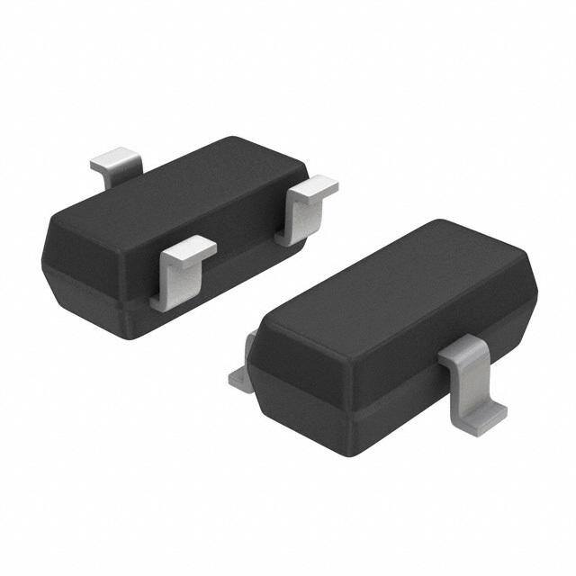
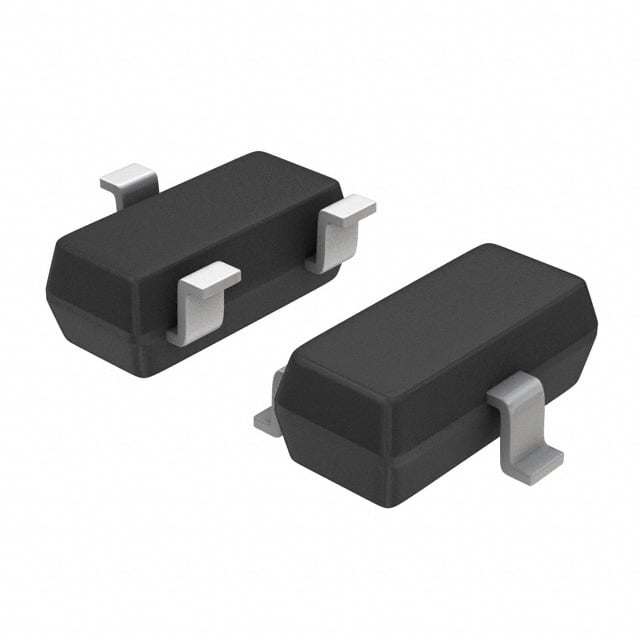
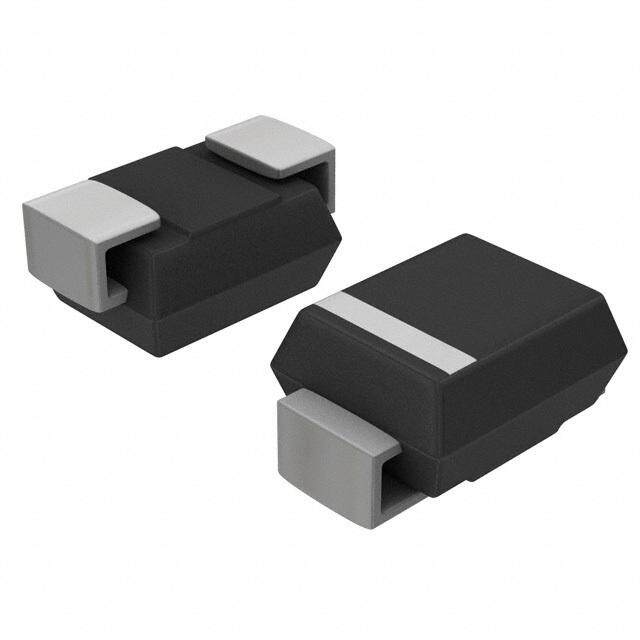
| 描述 | TVS DIODE 5.5VWM 8VC SOT23-3ESD 抑制器 Zener Diode |
| 产品分类 | |
| 品牌 | ON Semiconductor |
| 产品手册 | |
| 产品图片 |
|
| rohs | 符合RoHS无铅 / 符合限制有害物质指令(RoHS)规范要求 |
| 产品系列 | ON Semiconductor PACDN042Y3R- |
| 数据手册 | |
| 产品型号 | PACDN042Y3R |
| 不同频率时的电容 | - |
| 产品种类 | ESD 抑制器 |
| 供应商器件封装 | SOT-23-3(TO-236) |
| 其它名称 | PACDN042Y3R-ND |
| 功率-峰值脉冲 | - |
| 功率耗散Pd | 0.225 W |
| 包装 | 带卷 (TR) |
| 单向通道 | 2 |
| 双向通道 | - |
| 商标 | ON Semiconductor |
| 安装类型 | 表面贴装 |
| 封装 | Reel |
| 封装/外壳 | TO-236-3,SC-59,SOT-23-3 |
| 封装/箱体 | SOT-23-3 |
| 工作温度 | -40°C ~ 85°C (TA) |
| 工作温度范围 | - 40 C to + 85 C |
| 工厂包装数量 | 3000 |
| 应用 | 通用 |
| 标准包装 | 3,000 |
| 电压-击穿(最小值) | 6.2V |
| 电压-反向关态(典型值) | 5.5V |
| 电压-箝位(最大值)@Ipp | 8V |
| 电容 | 30 pF |
| 电流-峰值脉冲(10/1000µs) | - |
| 电源线路保护 | 无 |
| 端接类型 | SMD/SMT |
| 类型 | 齐纳 |
| 系列 | PACDN042 |
| 钳位电压 | 6.8 V / - 0.8 V |


- 商务部:美国ITC正式对集成电路等产品启动337调查
- 曝三星4nm工艺存在良率问题 高通将骁龙8 Gen1或转产台积电
- 太阳诱电将投资9.5亿元在常州建新厂生产MLCC 预计2023年完工
- 英特尔发布欧洲新工厂建设计划 深化IDM 2.0 战略
- 台积电先进制程称霸业界 有大客户加持明年业绩稳了
- 达到5530亿美元!SIA预计今年全球半导体销售额将创下新高
- 英特尔拟将自动驾驶子公司Mobileye上市 估值或超500亿美元
- 三星加码芯片和SET,合并消费电子和移动部门,撤换高东真等 CEO
- 三星电子宣布重大人事变动 还合并消费电子和移动部门
- 海关总署:前11个月进口集成电路产品价值2.52万亿元 增长14.8%


PDF Datasheet 数据手册内容提取
PACDN042 ESD Protection Diode Low Clamping Voltage Product Description The PACDN042/43/44/45/46 family of surge protection arrays www.onsemi.com provide a very high level of protection for sensitive electronic components that may be subjected to electrostatic discharge (ESD). The PACDN042/43/44/45/46 devices safely dissipate ESD strikes, exceeding the IEC 61000−4−2 International Standard, Level 4 (±8kV contact discharge). All pins are rated to withstand ±20kV ESD pulses SOT−23−3 SOT−23−5 SOT−23−6 using the IEC 61000−4−2 contact discharge method. Using the CASE 318 CASE 527AH CASE 527AJ MIL−STD−883D (Method 3015) specification for Human Body Model (HBM) ESD, all pins are protected from contact discharges of greater than ±30kV. Features • SOT−143 SC70−3 CS70−5 Two, Three, Four, Five, or Six surge protection CASE 527AF CASE 419AB CASE 419AC • Compact SMT Package Saves Board Space and Facilitates Layout in Space−Critical Applications • ± In−System ESD Protection to 20kV Contact Discharge, per the IEC61000−4−2 International Standard • These Devices are Pb−Free and are RoHS Compliant SC70−6 TSSOP8 MSOP8 CASE 419AD CASE 948AL CASE 846AB Applications • ESD Protection of PC Ports, Including USB Ports, Serial Ports, MARKING DIAGRAM Parallel Ports, IEEE1394 Ports, Docking Ports, Proprietary Ports, etc. • Protection of Interface Ports or IC Pins which are Exposed to High ESD Levels XXX M(cid:2) (cid:2) 1 XXX = Specific Device Code M = Date Code (cid:2) = Pb−Free Package (Note: Microdot may be in either location) ORDERING INFORMATION (see the last page of this document) © Semiconductor Components Industries, LLC, 2011 1 Publication Order Number: November, 2017 − Rev. 8 PACDN042/D
PACDN042 ELECTRICAL SCHEMATIC PACDN042 PACDN043 PACDN044T GND GND GND 3 4 3 8 7 6 5 1 2 1 2 1 2 3 4 GND GND GND SOT23−3 SOT−143 TSSOP−8 SC70−3 PACDN044Y PACDN045 PACDN046 GND 5 4 6 5 4 8 7 6 5 1 2 3 1 2 3 1 2 3 4 GND GND GND SOT23−5 SOT23−6 MSOP−8 SC70−5 SC70−6 PACKAGE / PINOUT DIAGRAMS Top View Top View Top View Cathode 1 Cathode 1 GND 1 4 Cathode 052 3 GND D52 3 GND D053 Cathode 2 Cathode 2 Cathode 2 3 Cathode 3−Pin SOT23 3−Pin SC70 4−Pin SOT−143 Top View Top View Top View GND 1 8 Cathode Cathode 1 5 Cathode Cathode 1 5 Cathode D D Cathode 2 PAC 7 GND GND 2 054 GND 2 54 GND 3 DN054T6 Cathode Cathode 3 4 Cathode Cathode 3 4 Cathode Cathode 4 5 GND 5−Pin SOT23 5−Pin SC70 8−Pin TSSOP Top View Top View Top View GND 1 8 GND CCaatthhooddee 1 6 Cathode Cathode 1 6 Cathode D D 5 Cathode 2 D 7 Cathode GND 2 05 5 Cathode GND 2 5/D 5 Cathode 05 5 5 Cathode 3 6 6 Cathode 6 CCaatthhooddee 3 4 Cathode Cathode 3 4 Cathode Cathode 4 5 Cathode 6−Pin SOT23 6−Pin SC70 8−Pin MSOP Note: SOT23, SC70, SOT−143, TSSOP, and MSOP Packages may differ in size. These drawings are not to scale. www.onsemi.com 2
PACDN042 Table 1. PIN DESCRIPTIONS Pins Name Description (Refer to Package Outline Drawings) Cathode The cathode of the respective surge protection diode, which should be connected to the node requiring transient voltage protection. (Refer to Package Outline Drawings) GND The anode of the surge protection diodes. SPECIFICATIONS Table 2. ABSOLUTE MAXIMUM RATINGS Parameter Rating Units Storage Temperature Range −65 to +150 °C Package Power Dissipation W SC70 0.2 SOT23−3, SOT23−5, SOT23−6, SOT−143 0.225 TSSOP, MSOP 0.5 Stresses exceeding those listed in the Maximum Ratings table may damage the device. If any of these limits are exceeded, device functionality should not be assumed, damage may occur and reliability may be affected. Table 3. STANDARD OPERATING CONDITIONS Parameter Rating Units Operating Temperature −40 to +85 °C Table 4. ELECTRICAL OPERATING CHARACTERISTICS Symbol Parameter Conditions Min Typ Max Units C Capacitance TA = 25°C, 2.5VDC, 1MHz 30 pF VRSO Reverse Stand−off Voltage IR = 10(cid:2)A, TA = 25°C 5.5 V IR = 1mA, TA = 25°C 6.1 V ILEAK Leakage Current VIN = 5.0VDC, TA = 25°C 1 100 nA VSIG Small Signal Clamp Voltage V Positive Clamp I = 10mA, TA = 25°C 6.2 6.8 8 Negative Clamp I = −10mA, TA = 25°C −0.4 −0.8 −1.2 VESD ESD Withstand Voltage kV Human Body Model, MIL−STD−883, (Note 1) ±30 Method 3015 Contact Discharge per IEC 61000−4−2 (Note 1) ±20 Standard RD Diode Dynamic Resistance (cid:3) Forward Conduction 1.0 Reverse Conduction 1.4 Product parametric performance is indicated in the Electrical Characteristics for the listed test conditions, unless otherwise noted. Product performance may not be indicated by the Electrical Characteristics if operated under different conditions. 1. ESD voltage applied between channel pins & ground, one pin at a time; all other channel pins open; all GND pins grounded. www.onsemi.com 3
PACDN042 PERFORMANCE INFORMATION Diode Capacitance Typical diode capacitance with respect to positive cathode voltage (reverse voltage across the diode) is given in Diode Capacitance vs. Reverse Voltage. Figure 1. Diode Capacitance vs. Reverse Voltage Typical High Current Diode Characteristics Measurements are made in pulse mode with a nominal pulse width of 0.7mS. Figure 2. Typical Input VI Characteristics (Pulse−mode measurements, pulse width = 0.7 mS nominal) www.onsemi.com 4
PACDN042 PACKAGE DIMENSIONS SOT−23 (TO−236) CASE 318−08 ISSUE AR D NOTES: 1. DIMENSIONING AND TOLERANCING PER ASME Y14.5M, 1994. 2. CONTROLLING DIMENSION: MILLIMETERS. 3. MAXIMUM LEAD THICKNESS INCLUDES LEAD FINISH. 0.25 MINIMUM LEAD THICKNESS IS THE MINIMUM THICKNESS OF 3 THE BASE MATERIAL. E HE T 4. DPRIMOETNRSUIOSINOSN DS, AONRD G EA DTEO BNUORTR INS.CLUDE MOLD FLASH, 1 2 MILLIMETERS INCHES DIM MIN NOM MAX MIN NOM MAX L A 0.89 1.00 1.11 0.035 0.039 0.044 3Xb L1 A1 0.01 0.06 0.10 0.000 0.002 0.004 b 0.37 0.44 0.50 0.015 0.017 0.020 e VIEW C c 0.08 0.14 0.20 0.003 0.006 0.008 TOP VIEW D 2.80 2.90 3.04 0.110 0.114 0.120 E 1.20 1.30 1.40 0.047 0.051 0.055 e 1.78 1.90 2.04 0.070 0.075 0.080 L 0.30 0.43 0.55 0.012 0.017 0.022 A L1 0.35 0.54 0.69 0.014 0.021 0.027 HE 2.10 2.40 2.64 0.083 0.094 0.104 T 0° −−− 10° 0° −−− 10° A1 c SIDE VIEW SEE VIEW C END VIEW RECOMMENDED SOLDERING FOOTPRINT* 3X 2.90 0.90 3X0.80 0.95 PITCH DIMENSIONS: MILLIMETERS *For additional information on our Pb−Free strategy and soldering details, please download the ON Semiconductor Soldering and Mounting Techniques Reference Manual, SOLDERRM/D. www.onsemi.com 5
PACDN042 PACKAGE DIMENSIONS SOT−23, 5 Lead CASE 527AH ISSUE O D SYMBOL MIN NOM MAX A 0.90 1.45 A1 0.00 0.15 A2 0.90 1.15 1.30 b 0.30 0.50 E1 E c 0.08 0.22 D 2.90 BSC E 2.80 BSC E1 1.60 BSC e 0.95 BSC e L 0.30 0.45 0.60 L1 0.60 REF PIN #1 IDENTIFICATION L2 0.25 REF TOP VIEW θ 0° 4° 8° θ1 5° 10° 15° θ2 5° 10° 15° θ1 A2 A θ b θ2 L1 L A1 L2 c SIDE VIEW END VIEW Notes: (1) All dimensions in millimeters. Angles in degrees. (2) Complies with JEDEC standard MO-178. www.onsemi.com 6
PACDN042 PACKAGE DIMENSIONS SOT−23, 6 Lead CASE 527AJ ISSUE B D A NOTES: B 1. DIMENSIONING AND TOLERANCING PER ASME Y14.5M, 1994. 2. CONTROLLING DIMENSION: MILLIMETERS. 3. DATUM C IS THE SEATING PLANE. 6 5 4 E E1 L2 MILLIMETERS DIM MIN MAX 1 2 3 GAGE A --- 1.45 PLANE A1 0.00 0.15 A2 0.90 1.30 e 6Xb L SPELAATNIENG bc 00..2008 00..5206 0.20 M C A S B S D 2.70 3.00 DETAIL A TOP VIEW E 2.50 3.10 E1 1.30 1.80 e 0.95 BSC A2 L 0.20 0.60 L2 0.25 BSC c A 6X 0.10 C DETAIL A A1 SIDE VIEW C SPELAATNIENG END VIEW RECOMMENDED SOLDERING FOOTPRINT* 3.30 6X 0.85 6X 0.56 0.95 PITCH DIMENSIONS: MILLIMETERS *For additional information on our Pb−Free strategy and soldering details, please download the ON Semiconductor Soldering and Mounting Techniques Reference Manual, SOLDERRM/D. www.onsemi.com 7
PACDN042 PACKAGE DIMENSIONS SOT−143, 4 Lead CASE 527AF ISSUE A SYMBOL MIN NOM MAX A 0.80 1.22 D A1 0.05 0.15 e A2 0.75 0.90 1.07 b 0.30 0.50 4 3 b2 0.76 0.89 c 0.08 0.20 D 2.80 2.90 3.04 E1 E E 2.10 2.64 E1 1.20 1.30 1.40 e 1.92 BSC 1 2 e1 0.20 BSC L 0.40 0.50 0.60 e1 b L1 0.54 REF L2 0.25 TOP VIEW θ 0° 8° A2 A (cid:4) c L2 b2 L A1 L1 SIDE VIEW END VIEW Notes: (1) All dimensions are in millimeters. Angles in degrees. (2) Complies with JEDEC TO-253. www.onsemi.com 8
PACDN042 PACKAGE DIMENSIONS SC−70, 3 Lead, 1.25x2 CASE 419AB ISSUE O SYMBOL MIN NOM MAX D A 0.80 1.10 A1 0.00 0.10 A2 0.80 0.90 1.00 b 0.15 0.30 c 0.08 0.22 E1 E D 1.80 2.00 2.20 E 1.80 2.10 2.40 E1 1.15 1.25 1.35 e 0.65 BSC L 0.26 0.36 0.46 e e L1 0.42 REF L2 0.15 BSC TOP VIEW θ 0º 8º θ1 4º 10º (cid:4)1 A2 A (cid:4) L b (cid:4)1 A1 L1 c L2 SIDE VIEW END VIEW Notes: (1) All dimensions are in millimeters. Angles in degrees. (2) Complies with JEDEC MO-203. www.onsemi.com 9
PACDN042 PACKAGE DIMENSIONS SC−88A (SC−70 5 Lead), 1.25x2 CASE 419AC ISSUE A SYMBOL MIN NOM MAX D A 0.80 1.10 e e A1 0.00 0.10 A2 0.80 1.00 b 0.15 0.30 c 0.10 0.18 D 1.80 2.00 2.20 E1 E E 1.80 2.10 2.40 E1 1.15 1.25 1.35 e 0.65 BSC L 0.26 0.36 0.46 L1 0.42 REF L2 0.15 BSC TOP VIEW θ 0º 8º θ1 4º 10º (cid:4)1 A2 A (cid:4) L b (cid:4)1 A1 L1 c L2 SIDE VIEW END VIEW Notes: (1) All dimensions are in millimeters. Angles in degrees. (2) Complies with JEDEC MO-203. www.onsemi.com 10
PACDN042 PACKAGE DIMENSIONS SC−88 (SC−70 6 Lead), 1.25x2 CASE 419AD ISSUE A SYMBOL MIN NOM MAX D A 0.80 1.10 e e A1 0.00 0.10 A2 0.80 1.00 b 0.15 0.30 c 0.10 0.18 E1 E D 1.80 2.00 2.20 E 1.80 2.10 2.40 E1 1.15 1.25 1.35 e 0.65 BSC L 0.26 0.36 0.46 L1 0.42 REF L2 0.15 BSC TOP VIEW θ 0º 8º θ1 4º 10º (cid:4)1 A2 A (cid:4) L b (cid:4)1 A1 L1 c L2 SIDE VIEW END VIEW Notes: (1) All dimensions are in millimeters. Angles in degrees. (2) Complies with JEDEC MO-203. www.onsemi.com 11
PACDN042 PACKAGE DIMENSIONS TSSOP8, 4.4x3 CASE 948AL ISSUE O b SYMBOL MIN NOM MAX A 1.20 A1 0.05 0.15 A2 0.80 0.90 1.05 b 0.19 0.30 E1 E c 0.09 0.20 D 2.90 3.00 3.10 E 6.30 6.40 6.50 E1 4.30 4.40 4.50 e 0.65 BSC L 1.00 REF L1 0.50 0.60 0.75 θ 0º 8º e TOP VIEW D A2 A (cid:4)1 c A1 L1 L SIDE VIEW END VIEW Notes: (1) All dimensions are in millimeters. Angles in degrees. (2) Complies with JEDEC MO-153. www.onsemi.com 12
PACDN042 PACKAGE DIMENSIONS MSOP8 CASE 846AB ISSUE O DD NOTES: 1. DIMENSIONING AND TOLERANCING PER ANSI Y14.5M, 1982. 2. CONTROLLING DIMENSION: MILLIMETER. 3. DIMENSION A DOES NOT INCLUDE MOLD FLASH, PROTRUSIONS OR GATE HE E BURRS. MOLD FLASH, PROTRUSIONS OR GATE BURRS SHALL NOT EXCEED 0.15 (0.006) PER SIDE. 4. DIMENSION B DOES NOT INCLUDE INTERLEAD FLASH OR PROTRUSION. INTERLEAD FLASH OR PROTRUSION SHALL NOT EXCEED 0.25 (0.010) PER SIDE. 5. 846A-01 OBSOLETE, NEW STANDARD 846A-02. PIN 1 ID e MILLIMETERS INCHES DIM MIN NOM MAX MIN NOM MAX b8 PL A −− −− 1.10 −− −− 0.043 0.08 (0.003) M T B S A S A1 0.05 0.08 0.15 0.002 0.003 0.006 b 0.25 0.33 0.40 0.010 0.013 0.016 c 0.13 0.18 0.23 0.005 0.007 0.009 D 2.90 3.00 3.10 0.114 0.118 0.122 E 2.90 3.00 3.10 0.114 0.118 0.122 SEATING e 0.65 BSC 0.026 BSC −T− PLANE L 0.40 0.55 0.70 0.016 0.021 0.028 0.038 (0.0015) A HE 4.75 4.90 5.05 0.187 0.193 0.199 A1 c L SOLDERING FOOTPRINT* 1.04 0.38 8X0.041 0.015 8X 3.20 4.24 5.28 0.126 0.167 0.208 0.65 (cid:2) (cid:3) 6X0.0256 SCALE 8:1 mm inches *For additional information on our Pb−Free strategy and soldering details, please download the ON Semiconductor Soldering and Mounting Techniques Reference Manual, SOLDERRM/D. www.onsemi.com 13
PACDN042 ORDERING INFORMATION ORDERING INFORMATION (cont’d) Device Package Shipping Device Package Shipping PACDN042Y3R SOT23−3 3000/Tape & Reel PACDN044YB5R SC70−5 3000/Tape & Reel (Pb−Free) (Pb−Free) PACDN044Y5R SOT23−5 3000/Tape & Reel PACDN045YB6R SC70−6 3000/Tape & Reel (Pb−Free) (Pb−Free) PACDN045Y6R SOT23−6 3000/Tape & Reel PACDN045YB6R−R SC70−6 3000/Tape & Reel (Pb−Free) (Pb−Free) PACDN043Y4R SOT−143 3000/Tape & Reel PACDN044TR TSSOP8 2500/Tape & Reel (Pb−Free) (Pb−Free) PACDN042YB3R SC70−3 3000/Tape & Reel PACDN046MR MSOP8 4000/Tape & Reel (Pb−Free) (Pb−Free) ON Semiconductor and are trademarks of Semiconductor Components Industries, LLC dba ON Semiconductor or its subsidiaries in the United States and/or other countries. ON Semiconductor owns the rights to a number of patents, trademarks, copyrights, trade secrets, and other intellectual property. A listing of ON Semiconductor’s product/patent coverage may be accessed at www.onsemi.com/site/pdf/Patent−Marking.pdf. ON Semiconductor reserves the right to make changes without further notice to any products herein. ON Semiconductor makes no warranty, representation or guarantee regarding the suitability of its products for any particular purpose, nor does ON Semiconductor assume any liability arising out of the application or use of any product or circuit, and specifically disclaims any and all liability, including without limitation special, consequential or incidental damages. Buyer is responsible for its products and applications using ON Semiconductor products, including compliance with all laws, regulations and safety requirements or standards, regardless of any support or applications information provided by ON Semiconductor. “Typical” parameters which may be provided in ON Semiconductor data sheets and/or specifications can and do vary in different applications and actual performance may vary over time. All operating parameters, including “Typicals” must be validated for each customer application by customer’s technical experts. ON Semiconductor does not convey any license under its patent rights nor the rights of others. ON Semiconductor products are not designed, intended, or authorized for use as a critical component in life support systems or any FDA Class 3 medical devices or medical devices with a same or similar classification in a foreign jurisdiction or any devices intended for implantation in the human body. Should Buyer purchase or use ON Semiconductor products for any such unintended or unauthorized application, Buyer shall indemnify and hold ON Semiconductor and its officers, employees, subsidiaries, affiliates, and distributors harmless against all claims, costs, damages, and expenses, and reasonable attorney fees arising out of, directly or indirectly, any claim of personal injury or death associated with such unintended or unauthorized use, even if such claim alleges that ON Semiconductor was negligent regarding the design or manufacture of the part. ON Semiconductor is an Equal Opportunity/Affirmative Action Employer. This literature is subject to all applicable copyright laws and is not for resale in any manner. PUBLICATION ORDERING INFORMATION LITERATURE FULFILLMENT: N. American Technical Support: 800−282−9855 Toll Free ON Semiconductor Website: www.onsemi.com Literature Distribution Center for ON Semiconductor USA/Canada 19521 E. 32nd Pkwy, Aurora, Colorado 80011 USA Europe, Middle East and Africa Technical Support: Order Literature: http://www.onsemi.com/orderlit Phone: 303−675−2175 or 800−344−3860 Toll Free USA/Canada Phone: 421 33 790 2910 Fax: 303−675−2176 or 800−344−3867 Toll Free USA/Canada Japan Customer Focus Center For additional information, please contact your local Email: orderlit@onsemi.com Phone: 81−3−5817−1050 Sales Representative ◊ www.onsemi.com PACDN042/D 14
Mouser Electronics Authorized Distributor Click to View Pricing, Inventory, Delivery & Lifecycle Information: O N Semiconductor: PACDN042Y3R