 Datasheet下载
- 型号: SP3010-04UTG
- 制造商: Littelfuse
- 库位|库存: xxxx|xxxx
- 要求:
| 数量阶梯 | 香港交货 | 国内含税 |
| +xxxx | $xxxx | ¥xxxx |
查看当月历史价格
查看今年历史价格
SP3010-04UTG产品简介:
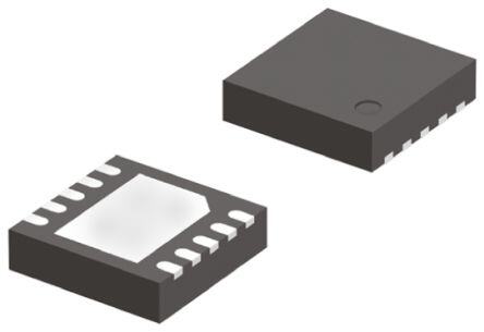
ICGOO电子元器件商城为您提供SP3010-04UTG由Littelfuse设计生产,在icgoo商城现货销售,并且可以通过原厂、代理商等渠道进行代购。 SP3010-04UTG价格参考。LittelfuseSP3010-04UTG封装/规格:TVS - 二极管, 12.3V (Typ) Clamp 3A (8/20µs) Ipp Tvs Diode Surface Mount 10-µDFN (2.5x1.0)。您可以下载SP3010-04UTG参考资料、Datasheet数据手册功能说明书,资料中有SP3010-04UTG 详细功能的应用电路图电压和使用方法及教程。
Littelfuse Inc. 的 SP3010-04UTG 是一款瞬态电压抑制(TVS)二极管阵列,属于TVS二极管类别,主要用于保护敏感电子设备免受瞬态电压冲击(如静电放电ESD、电快速瞬变脉冲群EFT和雷击感应浪涌)的损害。该器件采用小型化封装(SOT-23),集成四个独立的TVS二极管通道,适用于多线路信号保护。

SP3010-04UTG 的典型应用场景包括:

1. 消费类电子产品:广泛用于智能手机、平板电脑、笔记本电脑和USB接口等设备中,保护数据线(如USB 2.0、HDMI、音频接口)免受日常使用中的ESD损伤。

2. 通信接口保护:适用于RS-232、RS-485、以太网端口等工业或商用通信接口,提升系统在复杂电磁环境下的可靠性。

3. 便携式设备:因其小尺寸和低电容特性(每通道典型值小于1pF),非常适合高速信号线路保护,不影响信号完整性。

4. 工业控制与汽车电子辅助系统:用于保护车载信息娱乐系统、传感器接口和低电压控制电路,满足严苛环境下的抗干扰需求。

该器件具有低工作电压(最大6V)、高ESD防护能力(±15kV空气放电,±8kV接触放电,符合IEC 61000-4-2 Level 4标准),响应速度快(皮秒级),能有效钳制瞬态过压,保障后级IC安全。其紧凑设计有助于节省PCB空间,适合高密度布局产品。

综上,SP3010-04UTG 是适用于高速、低电压多通道接口的理想ESD保护解决方案,广泛应用于消费电子、通信、工业及车载周边等领域。
| 参数 | 数值 |
| 产品目录 | |
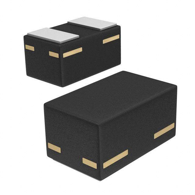
| 描述 | TVS DIODE 6VWM 12.3VC UDFNTVS二极管阵列 4 Ch 8kV 6V .45pF |
| 产品分类 | |
| 品牌 | Littelfuse |
| 产品手册 | |
| 产品图片 |
|
| rohs | 符合RoHS无铅 / 符合限制有害物质指令(RoHS)规范要求 |
| 产品系列 | 二极管与整流器,TVS二极管,TVS二极管阵列,Littelfuse SP3010-04UTGSP3010, SPA® |
| 数据手册 | |
| 产品型号 | SP3010-04UTG |
| 不同频率时的电容 | - |
| 产品培训模块 | http://www.digikey.cn/PTM/IndividualPTM.page?site=cn&lang=zhs&ptm=22970http://www.digikey.cn/PTM/IndividualPTM.page?site=cn&lang=zhs&ptm=25590 |
| 产品目录绘图 |
|
| 产品目录页面 | |
| 产品种类 | TVS二极管阵列 |
| 供应商器件封装 | 10-µDFN (2.5x1.0) |
| 其它名称 | F3507DKR |
| 击穿电压 | 6 V |
| 功率-峰值脉冲 | - |
| 包装 | Digi-Reel® |
| 单向通道 | - |
| 双向通道 | 4 |
| 商标 | Littelfuse |
| 商标名 | SPA |
| 安装类型 | 表面贴装 |
| 安装风格 | SMD/SMT |
| 封装 | Reel |
| 封装/外壳 | 10-UFDFN |
| 封装/箱体 | uDFN-10 |
| 尺寸 | 1 mm W x 2.5 mm L x 0.515 mm H |
| 峰值浪涌电流 | 3 A |
| 工作温度 | -40°C ~ 125°C |
| 工作电压 | 6 V |
| 工厂包装数量 | 3000 |
| 应用 | 通用 |
| 最大工作温度 | + 125 C |
| 最小工作温度 | - 55 C |
| 极性 | Bidirectional |
| 标准包装 | 1 |
| 特色产品 | http://www.digikey.com/cn/zh/ph/Littelfuse/SPA_Silicon_Protection.html |
| 电压-击穿(最小值) | - |
| 电压-反向关态(典型值) | 6V (最小值) |
| 电压-箝位(最大值)@Ipp | 12.3V (标准) |
| 电容 | 0.45 pF |
| 电流-峰值脉冲(10/1000µs) | 3A (8/20µs) |
| 电源线路保护 | 是 |
| 端接类型 | SMD/SMT |
| 类型 | 转向装置(轨至轨) |
| 系列 | SP3010 |
| 通道 | 4 Channels |
| 钳位电压 | 12.3 V |


- 商务部:美国ITC正式对集成电路等产品启动337调查
- 曝三星4nm工艺存在良率问题 高通将骁龙8 Gen1或转产台积电
- 太阳诱电将投资9.5亿元在常州建新厂生产MLCC 预计2023年完工
- 英特尔发布欧洲新工厂建设计划 深化IDM 2.0 战略
- 台积电先进制程称霸业界 有大客户加持明年业绩稳了
- 达到5530亿美元!SIA预计今年全球半导体销售额将创下新高
- 英特尔拟将自动驾驶子公司Mobileye上市 估值或超500亿美元
- 三星加码芯片和SET,合并消费电子和移动部门,撤换高东真等 CEO
- 三星电子宣布重大人事变动 还合并消费电子和移动部门
- 海关总署:前11个月进口集成电路产品价值2.52万亿元 增长14.8%


PDF Datasheet 数据手册内容提取
TVS Diode Arrays (SPA® Diodes) Low Capacitance ESD Protection - SP3010 Series SP3010 Series 0.45pF Diode Array RoHS Pb GREEN Description The SP3010 integrates 4 channels of ultra-low capacitance rail-to-rail diodes and an additional zener diode to provide protection for electronic equipment that may experience destructive electrostatic discharges (ESD). This robust device can safely absorb repetitive ESD strikes at the maximum level specified in the IEC 61000-4-2 international standard (Level 4, ±8kV contact discharge) without performance degradation. The extremely low loading capacitance also makes it ideal for protecting high speed signal pins such as HDMI, USB3.0, USB2.0, and IEEE 1394. Pinout Features • ESD, IEC 61000-4-2, • Low leakage current of 6 7 8 9 10 ±8kV contact, ±15kV air 0.1μA (TYP) at 5V • EFT, IEC 61000-4-4, 40A • Small form factor (5/50ns) μDFN( JEDEC MO-229) • Lightning, IEC 61000- package saves board 4-5 2nd edition, 3A space 5 4 3 2 1 (t =8/20μs) • RoHS compliant and P *Pins 6, 7, 9, 10 are not internally connected but should be connected to the trace. • Low capacitance of lead-free 0.45pF (TYP) per I/O Functional Block Diagram Applications • LCD/PDP TVs • Set Top Boxes • DVD Players • Mobile Phones • Desktops • Notebooks PPiinn 11 • MP3/PMP • Digital Cameras PPiinn 22 GGNNDD ((PPiinnss 33,,88)) PPiinn 44 PPiinn 55 Application Example HDMI HDMI Port Chipset D2+ Additional Information Ground D2- SP3010-04 D1+ Ground d D1- orl W Datasheet Resources Samples de D0+ si Ground ut D0- O SP3010-04 CLK+ Ground CLK- * Package is shown as transparent Case Life Support Note: Ground Signal Ground Not Intended for Use in Life Support or Life Saving Applications The products shown herein are not designed for use in life sustaining or life saving applications unless otherwise expressly indicated. © 2017 Littelfuse, Inc. Specifications are subject to change without notice. Revised: 02/23/17
TVS Diode Arrays (SPA® Diodes) Low Capacitance ESD Protection - SP3010 Series Absolute Maximum Ratings Symbol Parameter Value Units I Peak Current (t=8/20μs) 3.0 A PP p T Operating Temperature –40 to 125 °C OP T Storage Temperature –55 to 150 °C STOR CAUTION: Stresses above those listed in “Absolute Maximum Ratings” may cause permanent damage to the device. This is a stress only rating and operation of the device at these or any other conditions above those indicated in the operational sections of this specification is not implied. Electrical Characteristics (T =25ºC) OP Parameter Symbol Test Conditions Min Typ Max Units Reverse Standoff Voltage V I ≤ 1µA 6.0 V RWM R Reverse Leakage Current I V =5V, Any I/O to GND 0.1 0.5 µA LEAK R I =1A, t=8/20µs, Fwd 10.8 V Clamp Voltage1 V PP p C I =2A, t=8/20µs, Fwd 12.3 V PP p Dynamic Resistance R (V - V ) / (I - I ) 1.5 Ω DYN C2 C1 PP2 PP1 IEC61000-4-2 (Contact) ±8 kV ESD Withstand Voltage1 V ESD IEC61000-4-2 (Air) ±15 kV Diode Capacitance1 C Reverse Bias=0V 0.45 pF I/O-GND Note: 1 Parameter is guaranteed by design and/or device characterization. Capacitance vs. Bias Voltage Insertion Loss (S21) I/O to GND 0.6 0 0.5 -5 acitance (pF)00..34 nuation (dB)--1150 O Cap0.2 Atte-20 I/ 0.1 -25 0.0 -30 0.0 0.5 1.0 1.5 2.0 2.5 3.0 3.5 4.0 4.5 5.0 10 100 1000 10000 I/O Bias Voltage (V) Frequency (MHz) Clamping Voltage vs. I Pulse Waveform PP 16.0 110% 100% 14.0 90% V)C12.0 80% Voltage ( 108..00 nt of IPP 567000%%% Clamp 6.0 Perce 3400%% 4.0 20% 2.0 10% 0% 0.0 0.0 5.0 10.0 15.0 20.0 25.0 30.0 1.0 1.5 2.0 2.5 3.0 Time (μs) Peak Pulse Current-I (A) PP © 2017 Littelfuse, Inc. Specifications are subject to change without notice. Revised: 02/23/17
TVS Diode Arrays (SPA® Diodes) Low Capacitance ESD Protection - SP3010 Series Soldering Parameters Reflow Condition Pb – Free assembly tP TP CCrriittiiccaall ZZoonnee - Temperature Min (Ts(min)) 150°C e RRaammpp--uupp TTLL ttoo TTPP Pre Heat -- TTeimmep e(mraitnu rteo Mmaaxx )( T(ts()max)) 2600 0–° C180 secs rutare TS(mTaxL) tL s pm RRaammpp--ddoown Average ramp up rate (Liquidus) Temp e PPrreehheeaatt 3°C/second max T (TL) to peak TS(min) tS T to T - Ramp-up Rate 3°C/second max S(max) L Reflow -- TTeemmppeerraattuurree ((TtL)) (Liquidus) 26107 –° C1 50 seconds 25 time to peak temperature Time L Peak Temperature (T ) 260+0/-5 °C P Time within 5°C of actual peak 20 – 40 seconds Temperature (t ) p Ramp-down Rate 6°C/second max Time 25°C to peak Temperature (T ) 8 minutes Max. P Do not exceed 260°C Part Numbering System Product Characteristics SP 3010 04 U T G Lead Plating Pre-Plated Frame TVS Diode Arrays Lead Material Copper Alloy (SPA® Diodes) G= Green Lead Coplanarity 0.0004 inches (0.102mm) T= Tape & Reel Series Substitute Material Silicon Package Number of Channels µDFN-10 (2.5x1.0mm) Body Material Molded Epoxy -04 = 4 Channel Flammability UL 94 V-0 Notes : 1. All dimensions are in millimeters Part Marking System 2. Dimensions include solder plating. 3. Dimensions are exclusive of mold flash & metal burr. Q* 4 4. Blo is facing up for mold and facing down for trim/form, i.e. reverse trim/form. 5. Package surface matte finish VDI 11-13. Product Series Number of Q = SP3010 Channels Assembly Site Ordering Information Part Number Package Marking Min. Order Qty. SP3010-04UTG µDFN-10 Q*4 3000 © 2017 Littelfuse, Inc. Specifications are subject to change without notice. Revised: 02/23/17
TVS Diode Arrays (SPA® Diodes) Low Capacitance ESD Protection - SP3010 Series Embossed Carrier Tape & Reel Specification — µDFN-10 P0 P1 D0 T User Feeding Direction Package µDFN-10 (2.5x1.0x0.5mm) P2 Symbol Millimeters E A0 1.30 ± 0.10 B0 2.83 ± 0.10 W D0 Ø 1.50 + 0.10 D1 Ø 1.00 + 0.25 F E 1.75 ± 0.10 Top View D1 B0 5º Max Pin 1 Location F 3.50 ± 0.05 D A K0 0.65 ± 0.10 P0 4.00 ± 0.10 A0 P1 4.00 ± 0.10 E P2 2.00 ± 0.05 5º Max T 0.254 ± 0.02 0 B W 8.00 + 0.30 /- 0.10 K Side View Package Dimensions — µDFN-10 (2.5x1.0x0.5mm) 0.05 C A1 A3 A Seating Plane Package b1 µDFN0-1.005 (2C.5x1.0x0.5mm) C JEDEC b MO-229 Top View Millimeters Inches A Symbol 0.10M CAB D Min Nom Max Min Nom Max 0.05M C A 0.48 0.515 0.55 0.019 0.020 0.021 A1 0.00 -- 0.05 0.000 0.022 E A3 Bottom View0.125 Ref 0.005 Ref b R0.102.155 0.20 0.25 0.006 0.008 0.012 b1 0.35 0.40 0.45 0.014 0.016 0.018 B D 2.40 2.50 2.60 0.094 0.098 0.102 Side View LE 0.90 1.00 1.10 0.035 0.039 0.043 0.05 C A1 A3 e 2xR0.075m0.m50 ( 7BxS)C 0.020 BSC L e 0.30 0.365 0.43 0.012 0.014 0.016 A Seating Plane b1 0.05 C Recomended Soldering Pad Layout Dimensions C b Soldering Pad Layout Inch Millimeter P1 0.10M C AB P C (0.034) (0.875) G 0.008 0.20 0.05M C Y P 0.020 0.50 Z (C) G (Y1) P1 0.039 1.00 X 0.008 0.20 Bottom View X1 0.016 0.40 X R0.125 X1 Y 0.027 0.675 Y1 (0.061) (1.55) Alternative Z 0.061 1.55 L Soldering Pad Layout 2xR0.075mm (7x) P1 e P Y Recomended Z (C) G (Y1) Soldering Pad Layout P1 X P X1 Disclaimer Notice - Information furnished is believed to be accurate and reliable. However, users should independently evaluate the suitability of and test each product selected for their own Yapplications. Littelfuse products are not designed for, and may not be used in, all applications. Read comZpl(eCt)e DGisclaimer Notice at www.l(Yit1te)lfuse.com/disclaimer-electronics. © 2017 Littelfuse, Inc. Specifications are subject to change without notice. Revised: 02/23/17 X X1