ICGOO在线商城 > 射频/IF 和 RFID > RF 其它 IC 和模块 > HMC483MS8GE
 Datasheet下载
- 型号: HMC483MS8GE
- 制造商: Hittite
- 库位|库存: xxxx|xxxx
- 要求:
| 数量阶梯 | 香港交货 | 国内含税 |
| +xxxx | $xxxx | ¥xxxx |
查看当月历史价格
查看今年历史价格
HMC483MS8GE产品简介:
ICGOO电子元器件商城为您提供HMC483MS8GE由Hittite设计生产,在icgoo商城现货销售,并且可以通过原厂、代理商等渠道进行代购。 HMC483MS8GE价格参考。HittiteHMC483MS8GE封装/规格:RF 其它 IC 和模块, RF IC LO Amplifier, Mixer General Purpose 700MHz ~ 1.5GHz 8-MSOP。您可以下载HMC483MS8GE参考资料、Datasheet数据手册功能说明书,资料中有HMC483MS8GE 详细功能的应用电路图电压和使用方法及教程。
HMC483MS8GE是由Analog Devices Inc.(ADI公司)生产的一款RF(射频)IC,属于RF 其它 IC 和模块类别。该器件主要用于射频信号处理和无线通信系统中,具有高集成度、低噪声和宽频带特性,适用于多种应用场景。

1. 通信基础设施:HMC483MS8GE广泛应用于基站、微波回传设备和卫星通信系统中。它能够提供稳定的频率合成和信号调理功能,确保通信链路的可靠性和高效性。在5G通信网络中,它可以用于毫米波频段的信号处理,支持高速数据传输。

2. 雷达系统:该器件适用于各种雷达应用,包括气象雷达、空中交通管制雷达和军事雷达。其高频性能和低相位噪声特性使得它能够在复杂的电磁环境中保持高精度的信号检测和处理能力。

3. 测试与测量设备:HMC483MS8GE可用于高性能的射频测试仪器,如频谱分析仪、矢量信号发生器等。这些设备需要精确的频率控制和低噪声性能,以确保测试结果的准确性。

4. 无线传感器网络:在物联网(IoT)领域,HMC483MS8GE可以用于无线传感器节点中的射频前端设计。它能够提供高效的信号放大和调制功能,支持低功耗和长距离通信,适用于环境监测、智能农业等领域。

5. 航空航天与国防:在航空航天和国防应用中,HMC483MS8GE凭借其优异的射频性能和可靠性,被用于导航系统、电子战设备和机载通信系统中。它能够在极端环境下稳定工作,满足严苛的应用要求。

总之,HMC483MS8GE是一款高性能的射频IC,适用于广泛的通信、雷达、测试测量和国防等领域。其卓越的射频性能和低噪声特性使其成为许多关键应用的理想选择。
| 参数 | 数值 |
| 产品目录 | |
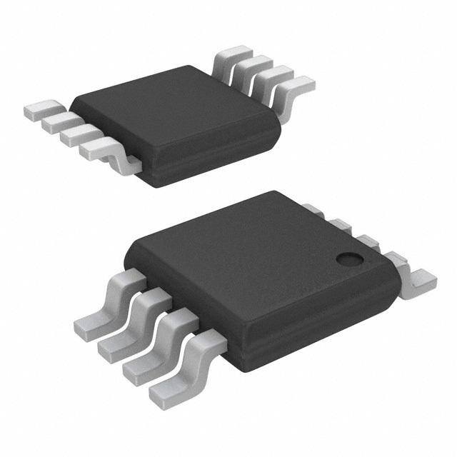
| 描述 | RF MIXER W/LO AMP 1.5GHZ 8MSOP |
| 产品分类 | |
| 品牌 | Hittite Microwave Corporation |
| 数据手册 | |
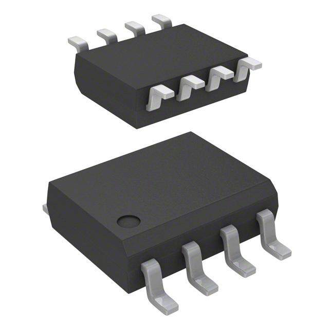
| 产品图片 |
|
| 产品型号 | HMC483MS8GE |
| RF类型 | 通用 |
| rohs | 无铅 / 符合限制有害物质指令(RoHS)规范要求 |
| 产品系列 | - |
| 供应商器件封装 | 8-MSOP |
| 其它名称 | 1127-1190-1 |
| 功能 | LO 放大器,混频器 |
| 包装 | 剪切带 (CT) |
| 封装/外壳 | 8-TSSOP,8-MSOP(0.118",3.00mm 宽)裸焊盘 |
| 标准包装 | 1 |
| 辅助属性 | - |
| 频率 | 700MHz ~ 1.5GHz |


- 商务部:美国ITC正式对集成电路等产品启动337调查
- 曝三星4nm工艺存在良率问题 高通将骁龙8 Gen1或转产台积电
- 太阳诱电将投资9.5亿元在常州建新厂生产MLCC 预计2023年完工
- 英特尔发布欧洲新工厂建设计划 深化IDM 2.0 战略
- 台积电先进制程称霸业界 有大客户加持明年业绩稳了
- 达到5530亿美元!SIA预计今年全球半导体销售额将创下新高
- 英特尔拟将自动驾驶子公司Mobileye上市 估值或超500亿美元
- 三星加码芯片和SET,合并消费电子和移动部门,撤换高东真等 CEO
- 三星电子宣布重大人事变动 还合并消费电子和移动部门
- 海关总署:前11个月进口集成电路产品价值2.52万亿元 增长14.8%


PDF Datasheet 数据手册内容提取
HMC483MS8G 483MS8GE / v01.0710 HIGH IP3 GaAs MMIC MIXER with INTEGRATED LO AMPLIFIER, 0.7 - 1.5 GHz Typical Applications Features The HMC483MS8G / HMC483MS8GE is ideal for: +33 dBm Input IP3 • Cellular/3G Conversion Loss: 9 dB 10 • GSM, GPRS & EDGE Low LO Drive: -4 to +4 dBm E • CDMA & WCDMA Single Positive Supply: 5V @ 50 mA • Cable Modem Termination Systems Ultra Small MSOP Package: 14.8mm2 T Included in the HMC-DK003 Designer’s Kit M T S - Functional Diagram General Description E 3 P The HMC483MS8G & HMC483MS8GE are high dy- I namic range passive MMIC mixers with integrated H LO Lamplifi ers in plastic surface mount 8 lead Mini G Small Outline Packages (MSOP) covering 0.7 to 1.5 HI GHz. Excellent input IP3 performance of +33 dBm O for down conversion and +30 dBm for up conversion - is provided for 2.5G & 3G GSM/CDMA applications S at an LO drive of 0 dBm. With an input 1 dB compression R of +24 dBm, the RF port will accept a wide range of E X S input signal levels. Conversion loss is 9 dB typical. I The DC to 350 MHz IF frequency response will satisfy M GSM/CDMA transmit or receive frequency plans confi gured for low side LO. The HMC483MS8G(E) B are pin for pin compatible with the HMC485MS8G(E) which are 1.7 - 2.2 GHz mixers with LO amplifi ers. O Electrical Specifi cations, T = +25°C, LO = 0 dBm, IF = 70 MHz*, Vdd= 5V A Parameter Min. Typ. Max. Min. Typ. Max. Units Frequency Range, RF & LO 0.8 - 1.1 0.7 - 1.5 GHz Frequency Range, IF DC - 350 DC - 350 MHz Conversion Loss 8.5 10.5 9 12 dB Noise Figure (SSB) 8.5 10.5 9 12 dB LO to RF Isolation 10 20 6 14 dB LO to IF Isolation 6 10 6 13 dB IP3 (Input) 33 33 dBm 1 dB Gain Compression (Input) 24 23 dBm LO Input Drive Level (Typical) -4 to +4 -4 to +4 dBm Supply Current 50 50 mA *Unless otherwise noted, all measurements performed as a downconverter. InforFmaotiro np fruircniseh,e dd beyl iAvnealroyg Daenvidce st ois pbelaliecveed otor dbee arcsc:u rHateit taintde reMliaibcler. oHwowaevveer, Cnoo rpFoorr aptriiocen,, d2e0liv Aerlyp, haand R too apdla,c Ce horedlemrss: fAonrdal,o gM DAe v0ic1e8s2, 4Inc., responsibility is assumed by Analog Devices for its use, nor for any infringements of patents or other One Technology Way, P.O. Box 9106, Norwood, MA 02062-9106 10 - 230 rliicgehntss eo fi sth girrda nptaerdti ebsy t himatp mlicaaPyt iorhenso uonlrt ofertoh:m e9r wit7sis 8ues -eu2.n dS5epr0e ca-inf3iyc 3aptia4otne3sn ts ou rb jpeFacttae tnoxt c:r hig9ahn7tgs 8eo wf- 2Aithn5oau0lot g-n 3oDti3ecve7i.c 3eNso . POhrodnee:r 7 O81n-3-2li9n-e4 7a0t0 w(cid:127) Owrwde.hr oitntliitnee. cato wmww.analog.com Trademarks and registered trademarks arAe tphep plriocpearttyi oof nth eSir urespppecotivret :o wPnehrso.ne: 978-250-3A3p4p3li c aotrio na Spuppsp@orht: iPtthitoen.ec: o1-m800-ANALOG-D
HMC483MS8G / 483MS8GE v01.0710 HIGH IP3 GaAs MMIC MIXER with INTEGRATED LO AMPLIFIER, 0.7 - 1.5 GHz Conversion Gain vs. Temperature Isolation 0 0 dB) -5 -10 10 AIN ( dB) E RSION G -10 LATION ( -20 VE + 25C SO T ON -15 + 85C I -30 TRLOF TTOO IRFF M C - 40C LO TO IF S -20 -40 - 0.6 0.7 0.8 0.9 1 1.1 1.2 1.3 1.4 1.5 0.6 0.7 E0.8 0.9 1 1.1 1.2 1.3 1.4 1.5 3 RF FREQUENCY (GHz) FREQUENCY (GHz) P I H L Conversion Gain vs. LO Drive Return Loss G I 0 0 H O - B) -5 -5 S AIN (d S (dB) R G S E SION -10 S RN LO -10 X ONVER -15 LLLOOO === ---642 dddBBBmmm RETU -15 LO MI C LO = 0 dBm RF LO = +2 dBm LO = +4 BdBm -20 -20 0.6 0.7 0.8 0.9 1 1.1 1.2 1.3 1.4 1.5 0.6 0.7 0.8 0.9 1 1.1 1.2 1.3 1.4 1.5 RF FREQUENCY (GHz) FREQUENCY (GHz) O Upconverter Performance Conversion Gain IF Bandwidth 0 0 B) -5 -5 CONVERSION GAIN d RETURN LOSS AIN ( dB) N G -10 SE ( -10 O N SI O R P ONVE -15 LLLOOO === ---642 dddBBBmmm RES -15 C LO = 0 dBm LO = +2 dBm LO = +4 dBm -20 -20 0.6 0.7 0.8 0.9 1 1.1 1.2 1.3 1.4 1.5 0 80 160 240 320 400 RF FREQUENCY (GHz) IF FREQUENCY (MHz) *Unless otherwise noted, all measurements performed as a downconverter, with low side LO & IF = 70 MHz. InforFmaotiro np fruircniseh,e dd beyl iAvnealroyg Daenvidce st ois pbelaliecveed otor dbee arcsc:u rHateit taintde reMliaibcler. oHwowaevveer, Cnoo rpFoorr aptriiocen,, d2e0liv Aerlyp, haand R too apdla,c Ce horedlemrss: fAonrdal,o gM DAe v0ic1e8s2, 4Inc., responsibility is assumed by Analog Devices for its use, nor for any infringements of patents or other One Technology Way, P.O. Box 9106, Norwood, MA 02062-9106 rights of third parties that maPy rhesounlt fero:m 9 it7s 8us-e2. S5p0ec-if3ic3ati4on3s s u b jeFcta tox c: h9an7g8e w-2ith5ou0t -n3oti3ce7. 3No POhrodnee:r 7 O81n-3-2li9n-e4 7a0t0 w(cid:127) Owrwde.hr oitntliitnee. cato wmww.analog.com 10 - 231 license is granted by implication or otherwise under any patent or patent rights of Analog Devices. Trademarks and registered trademarks arAe tphep plriocpearttyi oof nth eSir urespppecotivret :o wPnehrso.ne: 978-250-3A3p4p3li c aotrio na Spuppsp@orht: iPtthitoen.ec: o1-m800-ANALOG-D
HMC483MS8G / 483MS8GE v01.0710 HIGH IP3 GaAs MMIC MIXER with INTEGRATED LO AMPLIFIER, 0.7 - 1.5 GHz Input IP3 vs. Temperature Input IP3 vs. LO Drive 40 40 10 35 35 m) m) B B E d d P3 ( 30 P3 ( 30 T I T I U U MT INP 25 ++ 2855CC INP 25 TLLLOOO ===---642dddBBBmmm - 40C LO = 0dBm LO =+2dBm S LO =+4dBm 20 20 - 0.6 0.7 0.8 0.9 1 1.1 1.2 1.3 1.4 1.5 0.6 0.7 0E.8 0.9 1 1.1 1.2 1.3 1.4 1.5 3 FREQUENCY (GHz) FREQUENCY (GHz) P I H L G Input IP2 vs. Temperature Input IP2 vs. LO Drive I H 40 40 O - S 35 35 R Bm) m) MIXE NPUT IP2 (d 30 S PUT IP2 (dB 30 LO =-6dBm I 25 ++ 2855CC IN 25 LLOO ==--42ddBBmm - 40C LO = 0dBm B LLOO ==++24ddBBmm 20 20 0.6 0.7 0.8 0.9 1 1.1 1.2 1.3 1.4 1.5 0.6 0.7 0.8 0.9 1 1.1 1.2 1.3 1.4 1.5 FREQUENCY (GHz) FREQUENCY (GHz) O Input P1dB vs. Temperature Upconverter IP3 vs. LO Drive 30 40 25 30 m) B (dB dBm) P1d 20 P3 ( 20 LO =-6dBm UT UT I LLOO ==--42ddBBmm P P LO = 0dBm N + 25C N LO =+2dBm I 15 + 85C I 10 LO =+4dBm - 40C 10 0 0.6 0.7 0.8 0.9 1 1.1 1.2 1.3 1.4 1.5 0.7 0.8 0.9 1 1.1 1.2 1.3 1.4 1.5 FREQUENCY (GHz) RF FREQUENCY (GHz) InforFmaotiro np fruircniseh,e dd beyl iAvnealroyg Daenvidce st ois pbelaliecveed otor dbee arcsc:u rHateit taintde reMliaibcler. oHwowaevveer, Cnoo rpFoorr aptriiocen,, d2e0liv Aerlyp, haand R too apdla,c Ce horedlemrss: fAonrdal,o gM DAe v0ic1e8s2, 4Inc., responsibility is assumed by Analog Devices for its use, nor for any infringements of patents or other One Technology Way, P.O. Box 9106, Norwood, MA 02062-9106 10 - 232 rliicgehntss eo fi sth girrda nptaerdti ebsy t himatp mlicaaPyt iorhenso uonlrt ofertoh:m e9r wit7sis 8ues -eu2.n dS5epr0e ca-inf3iyc 3aptia4otne3sn ts ou rb jpeFacttae tnoxt c:r hig9ahn7tgs 8eo wf- 2Aithn5oau0lot g-n 3oDti3ecve7i.c 3eNso . POhrodnee:r 7 O81n-3-2li9n-e4 7a0t0 w(cid:127) Owrwde.hr oitntliitnee. cato wmww.analog.com Trademarks and registered trademarks arAe tphep plriocpearttyi oof nth eSir urespppecotivret :o wPnehrso.ne: 978-250-3A3p4p3li c aotrio na Spuppsp@orht: iPtthitoen.ec: o1-m800-ANALOG-D
HMC483MS8G / 483MS8GE v01.0710 HIGH IP3 GaAs MMIC MIXER with INTEGRATED LO AMPLIFIER, 0.7 - 1.5 GHz MxN Spurious Outputs Harmonics of LO nLO nLO Spur at RF Port mRF 0 1 2 3 4 LO Freq GHz 1 2 3 4 0 xx -9 24 3 16 0.7 21 23 24 25 10 1 4 0 30 15 28 0.8 15 23 18 43 E 2 66 71 50 61 61 0.9 12 26 23 39 3 83 95 103 89 95 1 9 22 33 32 4 106 105 103 108 108 1.1 6 22 42 27 T RF Freq = 0.87 GHz @ -10 dBm 1.2 3 T21 25 26 M LO Freq = 0.8 GHz @ 0 dBm LO power = 0 dBm All values in dBc Relative to the IF power level. All values in dBc below input LO level measured at RF port. S - Absolute Maximum Ratings E 3 P RF/IF Input +27 dBm LO Drive +10 dBm ELECTROSTATIC SENSITIVE DEVICE I H LOBSERVE HANDLING PRECAUTIONS Bias Supply (Vdd) +7 Vdc G Channel Temperature 150 °C I Continuous Pdiss (T = 85°C) H 0.58 W (Derate 8.95 mW/°C above 85°C) O - Thermal Resistance (RTH) 111.7 °C/W S (Channel to ground paddle) R Storage Temperature -65 to +150 °C E Operating Temperature -40 to +85 °C S X IF DC Current ±40 mA I ESD Sensitivity (HBM) Class 1B M Outline Drawing B O NOTES: 1. LEADFRAME MATERIAL: COPPER ALLOY 2. DIMENSIONS ARE IN INCHES [MILLIMETERS] 3. DIMENSION DOES NOT INCLUDE MOLDFLASH OF 0.15mm PER SIDE. 4. DIMENSION DOES NOT INCLUDE MOLDFLASH OF 0.25mm PER SIDE. 5. ALL GROUND LEADS AND GROUND PADDLE MUST BE SOLDERED TO PCB RF GROUND. InforFmaotiro np fruircniseh,e dd beyl iAvnealroyg Daenvidce st ois pbelaliecveed otor dbee arcsc:u rHateit taintde reMliaibcler. oHwowaevveer, Cnoo rpFoorr aptriiocen,, d2e0liv Aerlyp, haand R too apdla,c Ce horedlemrss: fAonrdal,o gM DAe v0ic1e8s2, 4Inc., responsibility is assumed by Analog Devices for its use, nor for any infringements of patents or other One Technology Way, P.O. Box 9106, Norwood, MA 02062-9106 rights of third parties that maPy rhesounlt fero:m 9 it7s 8us-e2. S5p0ec-if3ic3ati4on3s s u b jeFcta tox c: h9an7g8e w-2ith5ou0t -n3oti3ce7. 3No POhrodnee:r 7 O81n-3-2li9n-e4 7a0t0 w(cid:127) Owrwde.hr oitntliitnee. cato wmww.analog.com 10 - 233 license is granted by implication or otherwise under any patent or patent rights of Analog Devices. Trademarks and registered trademarks arAe tphep plriocpearttyi oof nth eSir urespppecotivret :o wPnehrso.ne: 978-250-3A3p4p3li c aotrio na Spuppsp@orht: iPtthitoen.ec: o1-m800-ANALOG-D
HMC483MS8G / 483MS8GE v01.0710 HIGH IP3 GaAs MMIC MIXER with INTEGRATED LO AMPLIFIER, 0.7 - 1.5 GHz Package Information Part Number Package Body Material Lead Finish MSL Rating Package Marking [3] HMC483MS8G Low Stress Injection Molded Plastic Sn/Pb Solder MSL1 [1] H483 XXXX 10 HMC483MS8GE RoHS-compliant Low Stress Injection Molded Plastic 100% matte Sn MSL1 [2] EXHX4X83X [1] Max peak refl ow temperature of 235 °C [2] Max peak refl ow temperature of 260 °C T [3] 4-Digit lot number XXXX M T S - E 3 P I H Pin Descriptions L G I Pin Number Function Description Interface Schematic H O - S This pin is AC coupled 1 LO R and matched to 50 Ohms. E X S MI 2 N/C Not connected. This pin may be connected to RF/DC ground without affecting performance. B This pin and the ground paddle must be 3, 6, 7 GND connected to RF ground. O Power supply for LO amplifi er. 4 Vdd An external RF bypass capacitor is required. This pin is DC coupled. For applications not requiring operation to DC this port should be DC blocked externally using a series capacitor. Choose value of capacitor to pass 5 IF IF frequency desired. For operation to DC, this pin must not sink/source more than 40 mA of current or failure may result. This pin is DC coupled 8 RF and matched to 50 Ohms. InforFmaotiro np fruircniseh,e dd beyl iAvnealroyg Daenvidce st ois pbelaliecveed otor dbee arcsc:u rHateit taintde reMliaibcler. oHwowaevveer, Cnoo rpFoorr aptriiocen,, d2e0liv Aerlyp, haand R too apdla,c Ce horedlemrss: fAonrdal,o gM DAe v0ic1e8s2, 4Inc., responsibility is assumed by Analog Devices for its use, nor for any infringements of patents or other One Technology Way, P.O. Box 9106, Norwood, MA 02062-9106 10 - 234 rliicgehntss eo fi sth girrda nptaerdti ebsy t himatp mlicaaPyt iorhenso uonlrt ofertoh:m e9r wit7sis 8ues -eu2.n dS5epr0e ca-inf3iyc 3aptia4otne3sn ts ou rb jpeFacttae tnoxt c:r hig9ahn7tgs 8eo wf- 2Aithn5oau0lot g-n 3oDti3ecve7i.c 3eNso . POhrodnee:r 7 O81n-3-2li9n-e4 7a0t0 w(cid:127) Owrwde.hr oitntliitnee. cato wmww.analog.com Trademarks and registered trademarks arAe tphep plriocpearttyi oof nth eSir urespppecotivret :o wPnehrso.ne: 978-250-3A3p4p3li c aotrio na Spuppsp@orht: iPtthitoen.ec: o1-m800-ANALOG-D
HMC483MS8G / 483MS8GE v01.0710 HIGH IP3 GaAs MMIC MIXER with INTEGRATED LO AMPLIFIER, 0.7 - 1.5 GHz Evaluation PCB 10 E T T M S - E 3 P I H L G I H O - S R E S X I M B O List of Materials for Evaluation PCB 105188 [1] The circuit board used in the application should use Item Description RF circuit design techniques. Signal lines should J1 - J3 PCB Mount SMA RF Connector have 50 Ohm impedance while the package ground J4 - J5 DC Pin leads and exposed paddle should be connected C1 10,000 pF Chip Capacitor, 0603 Pkg. directly to the ground plane similar to that shown. U1 HMC483MS8G / HMC483MS8GE Mixer A sufficient number of via holes should be used to PCB [2] 104813 Evaluation Board connect the top and bottom ground planes. The [1] Reference this number when ordering complete evaluation PCB evaluation circuit board shown is available from Hit- [2] Circuit Board Material: Rogers 4350 tite upon request. InforFmaotiro np fruircniseh,e dd beyl iAvnealroyg Daenvidce st ois pbelaliecveed otor dbee arcsc:u rHateit taintde reMliaibcler. oHwowaevveer, Cnoo rpFoorr aptriiocen,, d2e0liv Aerlyp, haand R too apdla,c Ce horedlemrss: fAonrdal,o gM DAe v0ic1e8s2, 4Inc., responsibility is assumed by Analog Devices for its use, nor for any infringements of patents or other One Technology Way, P.O. Box 9106, Norwood, MA 02062-9106 rights of third parties that maPy rhesounlt fero:m 9 it7s 8us-e2. S5p0ec-if3ic3ati4on3s s u b jeFcta tox c: h9an7g8e w-2ith5ou0t -n3oti3ce7. 3No POhrodnee:r 7 O81n-3-2li9n-e4 7a0t0 w(cid:127) Owrwde.hr oitntliitnee. cato wmww.analog.com 10 - 235 license is granted by implication or otherwise under any patent or patent rights of Analog Devices. Trademarks and registered trademarks arAe tphep plriocpearttyi oof nth eSir urespppecotivret :o wPnehrso.ne: 978-250-3A3p4p3li c aotrio na Spuppsp@orht: iPtthitoen.ec: o1-m800-ANALOG-D