ICGOO在线商城 > 射频/IF 和 RFID > RF 其它 IC 和模块 > HMC734LP5E
 Datasheet下载
- 型号: HMC734LP5E
- 制造商: Hittite
- 库位|库存: xxxx|xxxx
- 要求:
| 数量阶梯 | 香港交货 | 国内含税 |
| +xxxx | $xxxx | ¥xxxx |
查看当月历史价格
查看今年历史价格
HMC734LP5E产品简介:
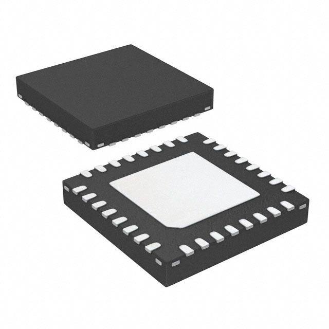
ICGOO电子元器件商城为您提供HMC734LP5E由Hittite设计生产,在icgoo商城现货销售,并且可以通过原厂、代理商等渠道进行代购。 HMC734LP5E价格参考。HittiteHMC734LP5E封装/规格:RF 其它 IC 和模块, RF IC VCO General Purpose 8.6GHz ~ 10.2GHz Dual Outputs (Divide by 4, Standard) 32-QFN (5x5)。您可以下载HMC734LP5E参考资料、Datasheet数据手册功能说明书,资料中有HMC734LP5E 详细功能的应用电路图电压和使用方法及教程。
HMC734LP5E 是由 Analog Devices Inc.(ADI)生产的一款 RF(射频)IC,具体属于倍频器类别。该器件具有出色的性能和集成度,广泛应用于需要高频信号生成的场景。以下是 HMC734LP5E 的主要应用场景:

1. 通信系统
   - 用于无线通信基础设施,如基站、中继站等,提供高频载波信号。
   - 在点对点无线电通信中,作为本地振荡器(LO)信号源或频率合成器的一部分。

2. 雷达系统
   - 在军事和民用雷达中,用作高频信号生成的核心组件,支持高精度的目标检测和跟踪。
   - 提供稳定的频率输出以满足多普勒雷达或其他类型雷达的需求。

3. 测试与测量设备
   - 应用于频谱分析仪、信号发生器和其他测试仪器中,用于生成精确的高频参考信号。
   - 支持宽频带测试需求,确保设备在不同频率范围内的性能评估准确可靠。

4. 卫星通信
   - 为卫星地面站和用户终端提供必要的高频信号支持。
   - 适用于 Ku 波段、Ka 波段等高频段的上变频和下变频操作。

5. 微波链路
   - 在微波回传网络中,用于扩展传输距离和提高数据速率。
   - 提供高效的频率转换功能,确保信号质量稳定。

6. 工业与科学应用
   - 在工业自动化、医疗成像等领域中,用作高频信号源,支持复杂的信号处理任务。
   - 例如,在核磁共振(NMR)或医学成像设备中,提供精确的射频激励信号。

HMC734LP5E 的工作频率范围为 DC 至 20 GHz,具备低相位噪声和高输出功率的特点,使其成为上述应用的理想选择。其紧凑的 5x5 mm LFCSP 封装也便于集成到各种高性能射频系统中。
| 参数 | 数值 |
| 产品目录 | |
| 描述 | IC MMIC VCO DIVIDE X4 32-QFN |
| 产品分类 | |
| 品牌 | Hittite Microwave Corporation |
| 数据手册 | |
| 产品图片 |
|
| 产品型号 | HMC734LP5E |
| RF类型 | 通用 |
| rohs | 无铅 / 符合限制有害物质指令(RoHS)规范要求 |
| 产品系列 | - |
| 供应商器件封装 | 32-QFN(5x5) |
| 其它名称 | 1127-1547 |
| 功能 | VCO |
| 包装 | 剪带 |
| 封装/外壳 | 32-VFQFN 裸露焊盘 |
| 标准包装 | 50 |
| 特色产品 | http://www.digikey.cn/product-highlights/zh/vcos/52289 |
| 辅助属性 | 双输出(除以 4,标准) |
| 频率 | 8.6GHz ~ 10.2GHz |


- 商务部:美国ITC正式对集成电路等产品启动337调查
- 曝三星4nm工艺存在良率问题 高通将骁龙8 Gen1或转产台积电
- 太阳诱电将投资9.5亿元在常州建新厂生产MLCC 预计2023年完工
- 英特尔发布欧洲新工厂建设计划 深化IDM 2.0 战略
- 台积电先进制程称霸业界 有大客户加持明年业绩稳了
- 达到5530亿美元!SIA预计今年全球半导体销售额将创下新高
- 英特尔拟将自动驾驶子公司Mobileye上市 估值或超500亿美元
- 三星加码芯片和SET,合并消费电子和移动部门,撤换高东真等 CEO
- 三星电子宣布重大人事变动 还合并消费电子和移动部门
- 海关总署:前11个月进口集成电路产品价值2.52万亿元 增长14.8%


PDF Datasheet 数据手册内容提取
HMC734LP5 734LP5E / v03.0609 MMIC VCO w/ DIVIDE-BY-4 8.6 - 10.2 GHz Typical Applications Features The HMC734LP5(E) is ideal for: Dual Output: Fo = 8.6 - 10.2 GHz Fo/4 = 2.15 - 2.55 GHz • Point-to-Point/Multi-Point Radio Pout: +18 dBm • Test Equipment & Industrial Controls Phase Noise: -100 dBc/Hz @ 100 kHz Typ. • SATCOM No External Resonator Needed • Military End-Use 32 Lead 5x5mm SMT Package: 25mm2 Functional Diagram General Description The HMC734LP5(E) is a GaAs InGaP Heterojunc- tion Bipolar Transistor (HBT) MMIC VCO. The HMC734LP5(E) integrates a resonator, negative resis- tance device, varactor diode and features a divide-by-4 frequency output. The VCO’s phase noise perfor- mance is excellent over temperature, shock, and pro- cess due to the oscillator’s monolithic structure. Power 8 output is +18 dBm typical from a +5V supply voltage. The prescaler function can be disabled to conserve current if not required. The voltage controlled oscilla- tor is packaged in a leadless QFN 5x5 mm surface T M mount package, and requires no external matching components. S - S O C V Electrical Specifications, T = +25° C, Vcc (Dig), Vcc (Amp), Vcc (RF) = +5V A Parameter Min. Typ. Max. Units Fo 8.6 - 10.2 GHz Frequency Range Fo/4 2.15 - 2.55 GHz RFOUT 15 22 dBm Power Output RFOUT/4 -8 -1 dBm SSB Phase Noise @ 100 kHz Offset, Vtune= +5V @ RFOUT -100 dBc/Hz Tune Voltage Vtune 1 13 V Supply Current Icc(Dig) + Icc(Amp) + Icc(RF) 180 218 240 mA Tune Port Leakage Current (Vtune= 13V) 10 µA Output Return Loss (RFOUT) 8 dB 1/2 66 Harmonics/Subharmonics dBc 2nd 15 dBc 3rd 30 Pulling (into a 2.0:1 VSWR) 38 MHz pp Pushing @ Vtune= 5V 30 MHz/V Frequency Drift Rate 1.1 MHz/°C InfoFrmoarti opn rfiucrneis,h edd eblyi vAenarlyog a Dnedvic etos isp blaelcieeve do trod beer asc:c uHraittet iatned Mreliiacbrleo. wHoawvevee r,C noo rpFoorra tpiroicne,, 2d0el iAvelrpyh, aan Rd otoa dpl,a cCeh oerldmerssf:o Arnda,l oMg AD e0v1ic8e2s4, Inc., responsibility is assumed by Analog Devices for its use, nor for any infringements of patents or other One Technology Way, P.O. Box 9106, Norwood, MA 02062-9106 8 - 1 rliicgehntss eo fi sth girrda nptaerdti ebsy t himatp mlicPaayht ioroens nuolret of:rto hm9er 7wits8is ue-s 2eu.n5 dS0epre- ca3infi3yc ap4tiao3tne sn ts ou rb Fjpeaactte xtno:t cr9higa7hnt8gs e-o 2wf Ai5thn0oaulo-t g3n oD3tiec7vei3.c eN s o. OPrhdoneer: O78n1--3li2n9e- 4a7t0 0w (cid:127)w Owrd.ehri totnitlein.ec aot mwww.analog.com Trademarks and registered trademarks aArep thpe lpircopaetrityo onf thSeiur rpesppeoctrivte: oPwhneorsn.e: 978-250-33A4p3p l icoart i oanp Spusp@pohrti:t Ptihteo.nceo: 1m-800-ANALOG-D
HMC734LP5 / 734LP5E v03.0609 MMIC VCO w/ DIVIDE-BY-4 8.6 - 10.2 GHz Frequency vs. Tuning Voltage, Vcc = +5V Frequency vs. Tuning Voltage, T= 25°C 11 11 10.6 10.6 z) z) H10.2 H10.2 G G Y ( 9.8 Y ( 9.8 C C EN 9.4 EN 9.4 U U Q 9 Q 9 E E R R F 8.6 +25C F 8.6 PUT 8.2 +-4805CC PUT 8.2 4.75V T T 5.00V OU 7.8 OU 7.8 5.25V 7.4 7.4 7 7 0 1 2 3 4 5 6 7 8 9 10 11 12 13 0 1 2 3 4 5 6 7 8 9 10 11 12 13 TUNING VOLTAGE (V) TUNING VOLTAGE (V) Output Power Sensitivity vs. Tuning Voltage, Vcc = +5V vs. Tuning Voltage, Vcc = +5V 700 25 8 600 Y(MHz/V)450000 ++-428055CCC WER (dBm) 1250 SITIVIT300 UT PO 10 ++2855CC MT SEN200 UTP -40C S O 5 100 - S 0 0 0 1 2 3 4 5 6 7 8 9 10 11 12 13 0 1 2 3 4 5 6 7 8 9 10 11 12 13 O Tuning Voltage (Volts) TUNING VOLTAGE (V) C V SSB Phase Noise vs. Tuning Voltage SSB Phase Noise @ Vtune = +5V -60 0 -20 z)-70 z) c/H c/H-40 +25C B B +85C E (d-80 E (d-60 -40C S S E NOI-90 11000kkhhzz E NOI-1-0800 S S A A H-100 H-120 P P SB SB -140 S-110 S -160 -120 -180 0 1 2 3 4 5 6 7 8 9 10 11 12 13 102 103 104 105 106 107 TUNING VOLTAGE (VOLTS) TUNING VOLTAGE (VOLTS) InfoFrmoarti opn rfiucrneis,h edd eblyi vAenarlyog a Dnedvic etos isp blaelcieeve do trod beer asc:c uHraittet iatned Mreliiacbrleo. wHoawvevee r,C noo rpFoorra tpiroicne,, 2d0el iAvelrpyh, aan Rd otoa dpl,a cCeh oerldmerssf:o Arnda,l oMg AD e0v1ic8e2s4, Inc., responsibility is assumed by Analog Devices for its use, nor for any infringements of patents or other One Technology Way, P.O. Box 9106, Norwood, MA 02062-9106 rights of third parties that mPayh roesnulet f:ro m9 7its8 u-s2e.5 S0pe-c3ifi3ca4tio3n s s u bFjeact xto: c9ha7n8ge- 2wi5th0ou-t 3no3tic7e3. N o OPrhdoneer: O78n1--3li2n9e- 4a7t0 0w (cid:127)w Owrd.ehri totnitlein.ec aot mwww.analog.com 8 - 2 license is granted by implication or otherwise under any patent or patent rights of Analog Devices. Trademarks and registered trademarks aArep thpe lpircopaetrityo onf thSeiur rpesppeoctrivte: oPwhneorsn.e: 978-250-33A4p3p l icoart i oanp Spusp@pohrti:t Ptihteo.nceo: 1m-800-ANALOG-D
HMC734LP5 / 734LP5E v03.0609 MMIC VCO w/ DIVIDE-BY-4 8.6 - 10.2 GHz Divide-by-4 Frequency Divide-by-4 Output Power vs. Tuning Voltage, Vcc = +5V vs. Tuning Voltage, Vcc = +5V 4 -1 GHz) 3.5 ++-428055CCC m) -2 NCY ( 3 R (dB -3 E E U W Q 2.5 O -4 E P UT FR 2 TPUT -5 P U UT O +25C O 1.5 -6 +85C -40C 1 -7 0 1 2 3 4 5 6 7 8 9 10 11 12 13 0 1 2 3 4 5 6 7 8 9 10 11 12 13 TUNING VOLTAGE (V) TUNING VOLTAGE (V) Outline Drawing 8 T M S - S O C V NOTES: 1. LEADFRAME MATERIAL: COPPER ALLOY 2. DIMENSIONS ARE IN INCHES [MILLIMETERS] 3. LEAD SPACING TOLERANCE IS NON-CUMULATIVE. 4. PAD BURR LENGTH SHALL BE 0.15mm MAXIMUM. PAD BURR HEIGHT SHALL BE 0.05mm MAXIMUM. 5. PACKAGE WARP SHALL NOT EXCEED 0.05mm. 6. ALL GROUND LEADS AND GROUND PADDLE MUST BE SOLDERED TO PCB RF GROUND. 7. REFER TO HITTITE APPLICATION NOTE FOR SUGGESTED LAND PATTERN. Package Information Part Number Package Body Material Lead Finish MSL Rating Package Marking [3] HMC734LP5 Low Stress Injection Molded Plastic Sn/Pb Solder MSL3 [1] H734 XXXX HMC734LP5E RoHS-compliant Low Stress Injection Molded Plastic 100% matte Sn MSL3 [2] H734 XXXX [1] Max peak reflow temperature of 235 °C [2] Max peak reflow temperature of 260 °C [3] 4-Digit lot number XXXX InfoFrmoarti opn rfiucrneis,h edd eblyi vAenarlyog a Dnedvic etos isp blaelcieeve do trod beer asc:c uHraittet iatned Mreliiacbrleo. wHoawvevee r,C noo rpFoorra tpiroicne,, 2d0el iAvelrpyh, aan Rd otoa dpl,a cCeh oerldmerssf:o Arnda,l oMg AD e0v1ic8e2s4, Inc., responsibility is assumed by Analog Devices for its use, nor for any infringements of patents or other One Technology Way, P.O. Box 9106, Norwood, MA 02062-9106 8 - 3 rliicgehntss eo fi sth girrda nptaerdti ebsy t himatp mlicPaayht ioroens nuolret of:rto hm9er 7wits8is ue-s 2eu.n5 dS0epre- ca3infi3yc ap4tiao3tne sn ts ou rb Fjpeaactte xtno:t cr9higa7hnt8gs e-o 2wf Ai5thn0oaulo-t g3n oD3tiec7vei3.c eN s o. OPrhdoneer: O78n1--3li2n9e- 4a7t0 0w (cid:127)w Owrd.ehri totnitlein.ec aot mwww.analog.com Trademarks and registered trademarks aArep thpe lpircopaetrityo onf thSeiur rpesppeoctrivte: oPwhneorsn.e: 978-250-33A4p3p l icoart i oanp Spusp@pohrti:t Ptihteo.nceo: 1m-800-ANALOG-D
HMC734LP5 / 734LP5E v03.0609 MMIC VCO w/ DIVIDE-BY-4 8.6 - 10.2 GHz Absolute Maximum Ratings Typical Supply Current vs. Vcc Vcc(Dig), Vcc(Amp), Vcc(RF) +5.5 Vdc Vcc (V) Icc (mA) Vtune 0 to +15V 4.75 198 Junction Temperature 135 °C 5.00 218 Continuous Pdiss (T=85 °C) 5.25 237 1.3 W (derate 25.3 mW/C above 85 °C Note: VCO will operate over full voltage range shown above. Thermal Resistance 39.5 °C/W (junction to ground paddle) ELECTROSTATIC SENSITIVE DEVICE Storage Temperature -65 to +150 °C OBSERVE HANDLING PRECAUTIONS Operating Temperature -40 to +85 °C Pin Descriptions Pin Number Function Description Interface Schematic 1 - 3, 7 - 10, No Connection. These pins may be connected to RF/ 12 - 17, 20, N/C DC ground. Performance will not be affected. 22 - 28, 30 - 32 8 4 RFOUT/4 Divide-by-4 output. DC block required. T M S - Supply voltage for prescaler. If prescaler is not S 6 Vcc (Dig) required, this pin may be left open to conserve approximately 100 mA of current. O C V 19 RFOUT RF output (AC coupled). 21 Vcc (RF) Supply Voltage, +5V Control voltage and modulation input. Modulation bandwidth dependent on drive source impedance. 29 VTUNE See “Determining the FM Bandwidth of a Wideband Varactor Tuned VCO” application note. 5, 11, 18, Package bottom has an exposed metal paddle that GND Paddle must be connected to RF/DC ground. InfoFrmoarti opn rfiucrneis,h edd eblyi vAenarlyog a Dnedvic etos isp blaelcieeve do trod beer asc:c uHraittet iatned Mreliiacbrleo. wHoawvevee r,C noo rpFoorra tpiroicne,, 2d0el iAvelrpyh, aan Rd otoa dpl,a cCeh oerldmerssf:o Arnda,l oMg AD e0v1ic8e2s4, Inc., responsibility is assumed by Analog Devices for its use, nor for any infringements of patents or other One Technology Way, P.O. Box 9106, Norwood, MA 02062-9106 rights of third parties that mPayh roesnulet f:ro m9 7its8 u-s2e.5 S0pe-c3ifi3ca4tio3n s s u bFjeact xto: c9ha7n8ge- 2wi5th0ou-t 3no3tic7e3. N o OPrhdoneer: O78n1--3li2n9e- 4a7t0 0w (cid:127)w Owrd.ehri totnitlein.ec aot mwww.analog.com 8 - 4 license is granted by implication or otherwise under any patent or patent rights of Analog Devices. Trademarks and registered trademarks aArep thpe lpircopaetrityo onf thSeiur rpesppeoctrivte: oPwhneorsn.e: 978-250-33A4p3p l icoart i oanp Spusp@pohrti:t Ptihteo.nceo: 1m-800-ANALOG-D
HMC734LP5 / 734LP5E v03.0609 MMIC VCO w/ DIVIDE-BY-4 8.6 - 10.2 GHz Application Circuit 8 T M S - S O C V InfoFrmoarti opn rfiucrneis,h edd eblyi vAenarlyog a Dnedvic etos isp blaelcieeve do trod beer asc:c uHraittet iatned Mreliiacbrleo. wHoawvevee r,C noo rpFoorra tpiroicne,, 2d0el iAvelrpyh, aan Rd otoa dpl,a cCeh oerldmerssf:o Arnda,l oMg AD e0v1ic8e2s4, Inc., responsibility is assumed by Analog Devices for its use, nor for any infringements of patents or other One Technology Way, P.O. Box 9106, Norwood, MA 02062-9106 8 - 5 rliicgehntss eo fi sth girrda nptaerdti ebsy t himatp mlicPaayht ioroens nuolret of:rto hm9er 7wits8is ue-s 2eu.n5 dS0epre- ca3infi3yc ap4tiao3tne sn ts ou rb Fjpeaactte xtno:t cr9higa7hnt8gs e-o 2wf Ai5thn0oaulo-t g3n oD3tiec7vei3.c eN s o. OPrhdoneer: O78n1--3li2n9e- 4a7t0 0w (cid:127)w Owrd.ehri totnitlein.ec aot mwww.analog.com Trademarks and registered trademarks aArep thpe lpircopaetrityo onf thSeiur rpesppeoctrivte: oPwhneorsn.e: 978-250-33A4p3p l icoart i oanp Spusp@pohrti:t Ptihteo.nceo: 1m-800-ANALOG-D
HMC734LP5 / 734LP5E v03.0609 MMIC VCO w/ DIVIDE-BY-4 8.6 - 10.2 GHz Evaluation PCB 8 T M S - S O C V List of Materials for Evaluation PCB 110227 [1] The circuit board used in the application should use Item Description RF circuit design techniques. Signal lines should J1 - J4 PCB Mount SMA RF Connector have 50 Ohm impedance while the package ground J5 - J6 2 mm DC Header leads and backside ground paddle should be con- C1 - C3 100 pF Capacitor, 0402 Pkg. nected directly to the ground plane similar to that C4 1,000 pF Capacitor, 0402 Pkg. shown. A sufficient number of via holes should be C5 - C7 2.2 µF Tantalum Capacitor used to connect the top and bottom ground planes. U1 HMC734LP5(E) VCO The evaluation circuit board shown is available from PCB [2] 110225 Eval Board Hittite upon request. [1] Reference this number when ordering complete evaluation PCB [2] Circuit Board Material: Rogers 4350 or Arlon 25FR InfoFrmoarti opn rfiucrneis,h edd eblyi vAenarlyog a Dnedvic etos isp blaelcieeve do trod beer asc:c uHraittet iatned Mreliiacbrleo. wHoawvevee r,C noo rpFoorra tpiroicne,, 2d0el iAvelrpyh, aan Rd otoa dpl,a cCeh oerldmerssf:o Arnda,l oMg AD e0v1ic8e2s4, Inc., responsibility is assumed by Analog Devices for its use, nor for any infringements of patents or other One Technology Way, P.O. Box 9106, Norwood, MA 02062-9106 rights of third parties that mPayh roesnulet f:ro m9 7its8 u-s2e.5 S0pe-c3ifi3ca4tio3n s s u bFjeact xto: c9ha7n8ge- 2wi5th0ou-t 3no3tic7e3. N o OPrhdoneer: O78n1--3li2n9e- 4a7t0 0w (cid:127)w Owrd.ehri totnitlein.ec aot mwww.analog.com 8 - 6 license is granted by implication or otherwise under any patent or patent rights of Analog Devices. Trademarks and registered trademarks aArep thpe lpircopaetrityo onf thSeiur rpesppeoctrivte: oPwhneorsn.e: 978-250-33A4p3p l icoart i oanp Spusp@pohrti:t Ptihteo.nceo: 1m-800-ANALOG-D