ICGOO在线商城 > 射频/IF 和 RFID > RF 其它 IC 和模块 > HMC447LC3TR
 Datasheet下载
- 型号: HMC447LC3TR
- 制造商: Hittite
- 库位|库存: xxxx|xxxx
- 要求:
| 数量阶梯 | 香港交货 | 国内含税 |
| +xxxx | $xxxx | ¥xxxx |
查看当月历史价格
查看今年历史价格
HMC447LC3TR产品简介:
ICGOO电子元器件商城为您提供HMC447LC3TR由Hittite设计生产,在icgoo商城现货销售,并且可以通过原厂、代理商等渠道进行代购。 HMC447LC3TR价格参考¥359.85-¥403.43。HittiteHMC447LC3TR封装/规格:RF 其它 IC 和模块, RF IC Divide-by-4 VSAT, DBS 10GHz ~ 26GHz 16-SMT (3x3)。您可以下载HMC447LC3TR参考资料、Datasheet数据手册功能说明书,资料中有HMC447LC3TR 详细功能的应用电路图电压和使用方法及教程。
HMC447LC3TR是Analog Devices Inc.(亚德诺半导体)旗下的一款射频(RF)集成电路,属于RF其它IC和模块类别。该器件是一款高线性度、低噪声的GaAs MMIC(单片微波集成电路)可变增益放大器(VGA),工作频率范围覆盖DC至2500 MHz,适用于多种宽带射频应用。

其主要应用场景包括:无线通信基础设施,如蜂窝基站中的接收链路和中频/射频信号调理;点对点微波通信系统中的中频放大与增益控制;军用和民用雷达系统中的前端信号处理;测试与测量设备,如频谱分析仪和信号发生器中的可调增益模块;以及需要高动态范围和优异线性性能的宽带接收机系统。

HMC447LC3TR具备优异的增益调节范围(典型值达40 dB)、低插入损耗和高三阶交调点(IP3),能够有效提升系统灵敏度和抗干扰能力。其采用紧凑的SOT-26封装,便于集成于空间受限的高频电路中。此外,该器件支持电压控制模式,可实现精确的增益调节,适合自动增益控制(AGC)环路设计。

综上所述,HMC447LC3TR广泛应用于对信号完整性要求较高的高性能射频系统中,尤其适用于需要宽频带、高线性度和稳定增益控制的通信与电子系统场景。
| 参数 | 数值 |
| 产品目录 | |
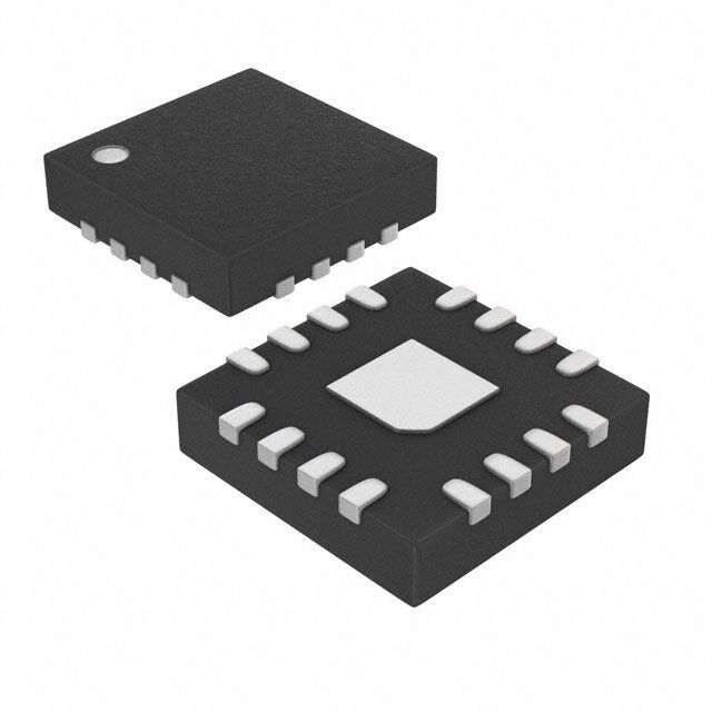
| 描述 | IC FREQ DIVIDER 10-26GHZ 16-QFN |
| 产品分类 | |
| 品牌 | Hittite Microwave Corporation |
| 数据手册 | |
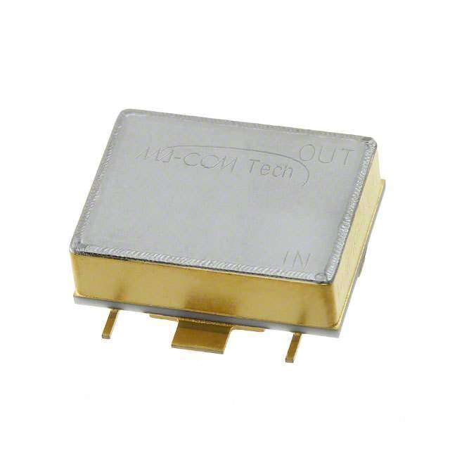
| 产品图片 |
|
| 产品型号 | HMC447LC3TR |
| RF类型 | VSAT,DBS |
| rohs | 无铅 / 符合限制有害物质指令(RoHS)规范要求 |
| 产品系列 | - |
| 供应商器件封装 | 16-SMT (3x3) |
| 其它名称 | 1127-1654-1 |
| 功能 | 除以 4 |
| 包装 | 剪切带 (CT) |
| 封装/外壳 | 16-VFQFN 裸露焊盘 |
| 标准包装 | 1 |
| 辅助属性 | - |
| 配用 | /product-detail/zh/107928-HMC447LC3/1127-2325-ND/4794621 |
| 频率 | 10GHz ~ 26GHz |


- 商务部:美国ITC正式对集成电路等产品启动337调查
- 曝三星4nm工艺存在良率问题 高通将骁龙8 Gen1或转产台积电
- 太阳诱电将投资9.5亿元在常州建新厂生产MLCC 预计2023年完工
- 英特尔发布欧洲新工厂建设计划 深化IDM 2.0 战略
- 台积电先进制程称霸业界 有大客户加持明年业绩稳了
- 达到5530亿美元!SIA预计今年全球半导体销售额将创下新高
- 英特尔拟将自动驾驶子公司Mobileye上市 估值或超500亿美元
- 三星加码芯片和SET,合并消费电子和移动部门,撤换高东真等 CEO
- 三星电子宣布重大人事变动 还合并消费电子和移动部门
- 海关总署:前11个月进口集成电路产品价值2.52万亿元 增长14.8%


PDF Datasheet 数据手册内容提取
HMC447LC3 v04.0514 SMT GaAs HBT MMIC DIVIDE-BY-4, 10 - 26 GHz Typical Applications Features Prescaler for 10 to 26 GHz PLL Applications: Very Wide Bandwidth T • Point-to-Point / Multi-Point Radios Ultra Low SSB Phase Noise: -150 dBc/Hz M • VSAT Radios Output Power: -4 dBm S • Fiber Optic Single DC Supply: +5V - S • Test Equipment RoHS Compliant 3x3 mm SMT Package R • Military O T Functional Diagram General Description C E The HMC447LC3 is a low noise Divide-by-4 T Regenerative Divider utilizing InGaP GaAs HBT E technology. This wideband divider operates with input D frequencies from 10 to 26 GHz, and accepts a very wide & range of input power levels. THe HMC447LC3 exhibits a very low SSB Phase Noise of -150 dBc/Hz at 100 kHz S offset, making it ideal for use in high frequency Phase R Locked Loops (PLL), and in Local Oscillator (LO) E D distribution applications where fundamental and I divided LO frequencies are required within a V system. This versatile divider consumes only 96 mA I D from a single positive supply of +5V, and delivers Y very flat output power across the rated bandwidth. C The HMC447LC3 is housed in a RoHS compliant, N 3x3 mm leadless SMT package with an exposed E ground paddle. U Q E R Electrical Specifications, T = +25° C, 50 Ohm System, Vcc= +5V A F Parameter Conditions Min. Typ. Max. Units Maximum Input Frequency 26 27 GHz Minimum Input Frequency 9 10 GHz Input Power Range Fin = 10 to 14 GHz -15 -20 +10 dBm Fin = 14 to 18 GHz -15 -20 +5 dBm Fin = 18 to 20 GHz -10 -15 +10 dBm Fin = 20 to 22 GHz -5 -10 +10 dBm Fin = 22 to 26 GHz 0 -5 +10 dBm Output Power Fin = 10 to 26 GHz -7 -4 dBm Reverse Leakage RF Output Terminated 50 dB SSB Phase Noise (100 kHz offset) Pin = 0 dBm, Fin = 22 GHz -150 dBc/Hz Output Transition Time Pin = 0 dBm, Fout = 4500 MHz 100 ps Supply Current (Icc1 + Icc2) 96 mA InfoFrmoart iopn rfiucrneis,h edde blyi vAenraylo ga Dnedvic teos ips lbaelcieeve do rtod beer sac:c Huraittet iatned Mreliiacbrleo. wHoawveeve rC, noo rpoForar tpioricne,, 2d eElilviezrayb, aentdh tDo rpivlaec,e C ohrdeelrms: sAfonardlo,g MDeAv i0ce1s8, 2In4c., responsibility is assumed by Analog Devices for its use, nor for any infringements of patents or other One Technology Way, P.O. Box 9106, Norwood, MA 02062-9106 1 rliicgehntss eo fi sth girrda nptaerdti ebsy t himatp mlicaaPyt iorhenso uonlrt ofertoh:m e9r wit7sis 8ues -eu2.n dS5ep0re ca-inf3iyc 3aptia4otne3sn ts ou rb jpeFacttae tnoxt c:r hig9ahn7tgs 8eo wf- 2Aithn5oau0lot g-n 3oDti3ecve7i.c 3eNso . POhrodnee:r 7 O81n-3-2li9n-e4 7a0t0 w(cid:127) wOrwde.hr oitntliitnee. cato wmww.analog.com Trademarks and registered trademarks arAe tphep plriocpearttyi oof nth eSir urespppecotivret :o wPnehrso.ne: 978-250-3A3p4p3li c aotrio na Spuppsp@orht: iPtthitoen.ec: o1-m800-ANALOG-D
HMC447LC3 v04.0514 SMT GaAs HBT MMIC DIVIDE-BY-4, 10 - 26 GHz Input Sensitivity Window, T= 25 °C Input Sensitivity Window vs. Temperature 20 20 15 15 T m) 10 m) 10 M B B d 5 d 5 Min Pin +25C S R ( Recommended R ( Max Pin +25C E 0 E 0 Min Pin +85C W Operating Window W Max Pin +85C - PO -5 PO -5 MMianx P Pinin --4400CC S T T PU-10 PU-10 R N N I-15 I-15 O -20 -20 T -25 -25 C 8 10 12 14 16 18 20 22 24 26 28 8 10 12 14 16 18 20 22 24 26 28 E INPUT FREQUENCY (GHz) INPUT FREQUENCY (GHz) T E D SSB Phase Noise Performance, Output Power vs. Temperature Pin= 0 dBm, Fin = 22 GHz, T= 25 °C & 0 0 S -20 R Bm) -2 Bc/Hz)-40 E WER (d -4 OISE (d-60 VID O N-80 OUTPUT P -6 +25C B PHASE --112000 Y DI -8 +85C S -40C S C -140 N -10 -160 8 12 16 20 24 28 102 103 104 105 106 E INPUT FREQUENCY (GHz) OFFSET FREQUENCY (Hz) U Q E Output Harmonic Content, Reverse Leakage, Pin= 0 dBm, T= 25 °C R Pin= 0 dBm, T= 25 °C Output Port Terminated F 0 0 Pfeedthru 2nd Harmonic -10 -10 3rd Harmonic m) m) B B-20 EL (d-20 EL (d-30 V V E E TPUT L-30 WER L-40 U O-50 O P -40 -60 -50 -70 8 10 12 14 16 18 20 22 24 26 28 8 10 12 14 16 18 20 22 24 26 28 INPUT FREQUENCY (GHz) INPUT FREQUENCY (GHz) InfoFrmoart iopn rfiucrneis,h edde blyi vAenraylo ga Dnedvic teos ips lbaelcieeve do rtod beer sac:c Huraittet iatned Mreliiacbrleo. wHoawveeve rC, noo rpoForar tpioricne,, 2d eElilviezrayb, aentdh tDo rpivlaec,e C ohrdeelrms: sAfonardlo,g MDeAv i0ce1s8, 2In4c., responsibility is assumed by Analog Devices for its use, nor for any infringements of patents or other One Technology Way, P.O. Box 9106, Norwood, MA 02062-9106 rights of third parties that maPy rhesounlt fero:m 9 it7s 8us-e2. S5p0ec-if3ic3ati4on3s s u b jeFcta tox c: h9an7g8e w-2ith5ou0t -n3oti3ce7. 3No POhrodnee:r 7 O81n-3-2li9n-e4 7a0t0 w(cid:127) wOrwde.hr oitntliitnee. cato wmww.analog.com 2 license is granted by implication or otherwise under any patent or patent rights of Analog Devices. Trademarks and registered trademarks arAe tphep plriocpearttyi oof nth eSir urespppecotivret :o wPnehrso.ne: 978-250-3A3p4p3li c aotrio na Spuppsp@orht: iPtthitoen.ec: o1-m800-ANALOG-D
HMC447LC3 v04.0514 SMT GaAs HBT MMIC DIVIDE-BY-4, 10 - 26 GHz Output Voltage Waveform, Pin= 0 dBm, Fout= 2.5 GHz, T= 25 °C Absolute Maximum Ratings 100 RF Input (Vcc = +5V) +13 dBm T Supply Voltage (Vcc1, Vcc2) +5.5V M 60 Junction Temperature (Tj) 135 °C V) S m Continuous Pdiss (T = 85 °C) DE ( 20 (derate 11.9 mW/° C above 85 °C) 595 mW - U T Thermal Resistance (R ) S PLI-20 (junction to ground padTdHle) 84 °C/W M R A Storage Temperature -65 to +150 °C O -60 Operating Temperature -40 to +85 °C T ESD Sensitivity (HBM) Class 1A C -100 E 22.7 22.9 23.1 23.3 23.5 23.7 Typical Supply Current vs. Vcc TIME (nS) T E Vcc1, Vcc2 (V) Icc (mA) D ELECTROSTATIC SENSITIVE DEVICE 4.75 84 OBSERVE HANDLING PRECAUTIONS 5.0 96 & 5.25 108 S Note: Divider will operate over full voltage range shown above R E D I V I D Y C N E U Q E R F InfoFrmoart iopn rfiucrneis,h edde blyi vAenraylo ga Dnedvic teos ips lbaelcieeve do rtod beer sac:c Huraittet iatned Mreliiacbrleo. wHoawveeve rC, noo rpoForar tpioricne,, 2d eElilviezrayb, aentdh tDo rpivlaec,e C ohrdeelrms: sAfonardlo,g MDeAv i0ce1s8, 2In4c., responsibility is assumed by Analog Devices for its use, nor for any infringements of patents or other One Technology Way, P.O. Box 9106, Norwood, MA 02062-9106 3 rliicgehntss eo fi sth girrda nptaerdti ebsy t himatp mlicaaPyt iorhenso uonlrt ofertoh:m e9r wit7sis 8ues -eu2.n dS5ep0re ca-inf3iyc 3aptia4otne3sn ts ou rb jpeFacttae tnoxt c:r hig9ahn7tgs 8eo wf- 2Aithn5oau0lot g-n 3oDti3ecve7i.c 3eNso . POhrodnee:r 7 O81n-3-2li9n-e4 7a0t0 w(cid:127) wOrwde.hr oitntliitnee. cato wmww.analog.com Trademarks and registered trademarks arAe tphep plriocpearttyi oof nth eSir urespppecotivret :o wPnehrso.ne: 978-250-3A3p4p3li c aotrio na Spuppsp@orht: iPtthitoen.ec: o1-m800-ANALOG-D
HMC447LC3 v04.0514 SMT GaAs HBT MMIC DIVIDE-BY-4, 10 - 26 GHz Outline Drawing T M S - S R O T C E T E D & NOTES: S 1. PACKAGE BODY MATERIAL: ALUMINA R 2. LEAD AND GROUND PADDLE PLATING: 30-80 MICROINCHES E GOLD OVER 50 MICROINCHES MINIMUM NICKEL. 3. DIMENSIONS ARE IN INCHES [MILLIMETERS] D 4. LEAD SPACING TOLERANCE IS NON-CUMULATIVE. I V 5. PACKAGE WARP SHALL NOT EXCEED 0.05mm DATUM -C- . 6. ALL GROUND LEADS AND GROUND PADDLE MUST BE DI SOLDERED TO PCB RF GROUND. Y C N E U Package Information Q Part Number Package Body Material Lead Finish MSL Rating Package Marking [2] E R HMC447LC3 Alumina, White Gold over Nickel MSL3 [1] XHX4X47X F [1] Max peak reflow temperature of 260 °C [2] 4-Digit lot number XXXX InfoFrmoart iopn rfiucrneis,h edde blyi vAenraylo ga Dnedvic teos ips lbaelcieeve do rtod beer sac:c Huraittet iatned Mreliiacbrleo. wHoawveeve rC, noo rpoForar tpioricne,, 2d eElilviezrayb, aentdh tDo rpivlaec,e C ohrdeelrms: sAfonardlo,g MDeAv i0ce1s8, 2In4c., responsibility is assumed by Analog Devices for its use, nor for any infringements of patents or other One Technology Way, P.O. Box 9106, Norwood, MA 02062-9106 rights of third parties that maPy rhesounlt fero:m 9 it7s 8us-e2. S5p0ec-if3ic3ati4on3s s u b jeFcta tox c: h9an7g8e w-2ith5ou0t -n3oti3ce7. 3No POhrodnee:r 7 O81n-3-2li9n-e4 7a0t0 w(cid:127) wOrwde.hr oitntliitnee. cato wmww.analog.com 4 license is granted by implication or otherwise under any patent or patent rights of Analog Devices. Trademarks and registered trademarks arAe tphep plriocpearttyi oof nth eSir urespppecotivret :o wPnehrso.ne: 978-250-3A3p4p3li c aotrio na Spuppsp@orht: iPtthitoen.ec: o1-m800-ANALOG-D
HMC447LC3 v04.0514 SMT GaAs HBT MMIC DIVIDE-BY-4, 10 - 26 GHz Pin Description Pin Number Function Description Interface Schematic T 1,2, 4 - 9, 11 No connection. These pins may be connected to RF/DC M N/C 12, 13, 16 ground. Performance will not be affected. S - S R 3 Fin RF Input must be DC blocked. O T C E T E 10 Fout Divided Output must be DC blocked. D & S R E 14, 15 Vcc1, Vcc2 Supply voltage 5V ± 0.25V. Connect both pins to +5V supply. D I V Backside of package has exposed metal ground paddle GND I which must be connected to RF/DC ground. D Y C N E U Q E R F InfoFrmoart iopn rfiucrneis,h edde blyi vAenraylo ga Dnedvic teos ips lbaelcieeve do rtod beer sac:c Huraittet iatned Mreliiacbrleo. wHoawveeve rC, noo rpoForar tpioricne,, 2d eElilviezrayb, aentdh tDo rpivlaec,e C ohrdeelrms: sAfonardlo,g MDeAv i0ce1s8, 2In4c., responsibility is assumed by Analog Devices for its use, nor for any infringements of patents or other One Technology Way, P.O. Box 9106, Norwood, MA 02062-9106 5 rliicgehntss eo fi sth girrda nptaerdti ebsy t himatp mlicaaPyt iorhenso uonlrt ofertoh:m e9r wit7sis 8ues -eu2.n dS5ep0re ca-inf3iyc 3aptia4otne3sn ts ou rb jpeFacttae tnoxt c:r hig9ahn7tgs 8eo wf- 2Aithn5oau0lot g-n 3oDti3ecve7i.c 3eNso . POhrodnee:r 7 O81n-3-2li9n-e4 7a0t0 w(cid:127) wOrwde.hr oitntliitnee. cato wmww.analog.com Trademarks and registered trademarks arAe tphep plriocpearttyi oof nth eSir urespppecotivret :o wPnehrso.ne: 978-250-3A3p4p3li c aotrio na Spuppsp@orht: iPtthitoen.ec: o1-m800-ANALOG-D
HMC447LC3 v04.0514 SMT GaAs HBT MMIC DIVIDE-BY-4, 10 - 26 GHz Evaluation PCB T M S - S R O T C E T E D & S R E D I V I D Y C N E U Q E List of Materials for Evaluation PCB 107928 [1] R F The circuit board used in the final application sho- Item Description uld use RF circuit design techniques. Signal lines J1 PCB Mount SRI K-Connector should have 50 Ohm impedance while the package J2 PCB Mount SMA RF Connector ground leads and backside ground paddle should J3, J4 DC Pin be connected directly to the ground plane similar C1 10pF Capacitor, 0402 Pkg. to that shown. A sufficient number of via holes C2, C3 100 pF Capacitor, 0402 Pkg. should be used to connect the top and bottom C4 10000 pF Capacitor, 0603 Pkg. ground planes. The evaluation circuit board shown C5 2.2 uF Tantalum Capacitor is available from Hittite upon request. U1 HMC447LC3 Divide-by-4 PCB [2] 107926 Eval Board [1] Reference this number when ordering complete evaluation PCB [2] Circuit Board Material: Rogers 4350 InfoFrmoart iopn rfiucrneis,h edde blyi vAenraylo ga Dnedvic teos ips lbaelcieeve do rtod beer sac:c Huraittet iatned Mreliiacbrleo. wHoawveeve rC, noo rpoForar tpioricne,, 2d eElilviezrayb, aentdh tDo rpivlaec,e C ohrdeelrms: sAfonardlo,g MDeAv i0ce1s8, 2In4c., responsibility is assumed by Analog Devices for its use, nor for any infringements of patents or other One Technology Way, P.O. Box 9106, Norwood, MA 02062-9106 rights of third parties that maPy rhesounlt fero:m 9 it7s 8us-e2. S5p0ec-if3ic3ati4on3s s u b jeFcta tox c: h9an7g8e w-2ith5ou0t -n3oti3ce7. 3No POhrodnee:r 7 O81n-3-2li9n-e4 7a0t0 w(cid:127) wOrwde.hr oitntliitnee. cato wmww.analog.com 6 license is granted by implication or otherwise under any patent or patent rights of Analog Devices. Trademarks and registered trademarks arAe tphep plriocpearttyi oof nth eSir urespppecotivret :o wPnehrso.ne: 978-250-3A3p4p3li c aotrio na Spuppsp@orht: iPtthitoen.ec: o1-m800-ANALOG-D
HMC447LC3 v04.0514 SMT GaAs HBT MMIC DIVIDE-BY-4, 10 - 26 GHz Application Circuit T M S - S R O T C E T E D & S R E D I V I D Y C N E U Q E R F InfoFrmoart iopn rfiucrneis,h edde blyi vAenraylo ga Dnedvic teos ips lbaelcieeve do rtod beer sac:c Huraittet iatned Mreliiacbrleo. wHoawveeve rC, noo rpoForar tpioricne,, 2d eElilviezrayb, aentdh tDo rpivlaec,e C ohrdeelrms: sAfonardlo,g MDeAv i0ce1s8, 2In4c., responsibility is assumed by Analog Devices for its use, nor for any infringements of patents or other One Technology Way, P.O. Box 9106, Norwood, MA 02062-9106 7 rliicgehntss eo fi sth girrda nptaerdti ebsy t himatp mlicaaPyt iorhenso uonlrt ofertoh:m e9r wit7sis 8ues -eu2.n dS5ep0re ca-inf3iyc 3aptia4otne3sn ts ou rb jpeFacttae tnoxt c:r hig9ahn7tgs 8eo wf- 2Aithn5oau0lot g-n 3oDti3ecve7i.c 3eNso . POhrodnee:r 7 O81n-3-2li9n-e4 7a0t0 w(cid:127) wOrwde.hr oitntliitnee. cato wmww.analog.com Trademarks and registered trademarks arAe tphep plriocpearttyi oof nth eSir urespppecotivret :o wPnehrso.ne: 978-250-3A3p4p3li c aotrio na Spuppsp@orht: iPtthitoen.ec: o1-m800-ANALOG-D
HMC447LC3 v04.0514 SMT GaAs HBT MMIC DIVIDE-BY-4, 10 - 26 GHz T M S - S R O T C E T E D & S R E D I V I D Y C N E U Q E R F InfoFrmoart iopn rfiucrneis,h edde blyi vAenraylo ga Dnedvic teos ips lbaelcieeve do rtod beer sac:c Huraittet iatned Mreliiacbrleo. wHoawveeve rC, noo rpoForar tpioricne,, 2d eElilviezrayb, aentdh tDo rpivlaec,e C ohrdeelrms: sAfonardlo,g MDeAv i0ce1s8, 2In4c., responsibility is assumed by Analog Devices for its use, nor for any infringements of patents or other One Technology Way, P.O. Box 9106, Norwood, MA 02062-9106 rights of third parties that maPy rhesounlt fero:m 9 it7s 8us-e2. S5p0ec-if3ic3ati4on3s s u b jeFcta tox c: h9an7g8e w-2ith5ou0t -n3oti3ce7. 3No POhrodnee:r 7 O81n-3-2li9n-e4 7a0t0 w(cid:127) wOrwde.hr oitntliitnee. cato wmww.analog.com 8 license is granted by implication or otherwise under any patent or patent rights of Analog Devices. Trademarks and registered trademarks arAe tphep plriocpearttyi oof nth eSir urespppecotivret :o wPnehrso.ne: 978-250-3A3p4p3li c aotrio na Spuppsp@orht: iPtthitoen.ec: o1-m800-ANALOG-D