ICGOO在线商城 > 射频/IF 和 RFID > RF 其它 IC 和模块 > TL852CDR
 Datasheet下载
- 型号: TL852CDR
- 制造商: Texas Instruments
- 库位|库存: xxxx|xxxx
- 要求:
| 数量阶梯 | 香港交货 | 国内含税 |
| +xxxx | $xxxx | ¥xxxx |
查看当月历史价格
查看今年历史价格
TL852CDR产品简介:
ICGOO电子元器件商城为您提供TL852CDR由Texas Instruments设计生产,在icgoo商城现货销售,并且可以通过原厂、代理商等渠道进行代购。 TL852CDR价格参考¥18.25-¥37.40。Texas InstrumentsTL852CDR封装/规格:RF 其它 IC 和模块, RF IC Sonar Ranging Receiver Sonar Control 20kHz ~ 90kHz TTL-Compatible 16-SOIC。您可以下载TL852CDR参考资料、Datasheet数据手册功能说明书,资料中有TL852CDR 详细功能的应用电路图电压和使用方法及教程。
TL852CDR 是 Texas Instruments(德州仪器)生产的一款双通道、低功耗运算放大器,虽然其主要分类属于通用运放,但在部分应用中可能被归类于RF相关模块或电路的辅助器件。需要注意的是,TL852CDR 并非专门的射频(RF)集成电路,因此在严格意义上的RF信号处理(如高频放大、混频、调制解调等)中并不常见。

该器件的主要应用场景包括:
1. 信号调理:在RF系统前端或后端用于对微弱信号进行放大和滤波,例如传感器信号或接收链路中的中频信号处理。
2. 音频与模拟接口:适用于通信设备中的音频输入/输出缓冲或电平转换电路。
3. 工业控制与测试设备:用于精密模拟信号处理,如数据采集系统中的放大环节。
4. 低频RF相关系统:在低速无线传感或低功耗物联网(IoT)节点中,配合主RF芯片完成偏置电路或监测功能。

TL852CDR 具有低失调电压、宽电源电压范围(2.7V 至 36V)和良好的稳定性,适合对精度和可靠性要求较高的场合。尽管不直接处理高频RF信号,但可作为支持性元件用于RF模块周边的模拟电路设计中。

总结:TL852CDR 主要应用于需要稳定、低噪声运算放大的场景,在RF系统中多用于辅助信号调理,而非核心射频功能。
| 参数 | 数值 |
| 产品目录 | |
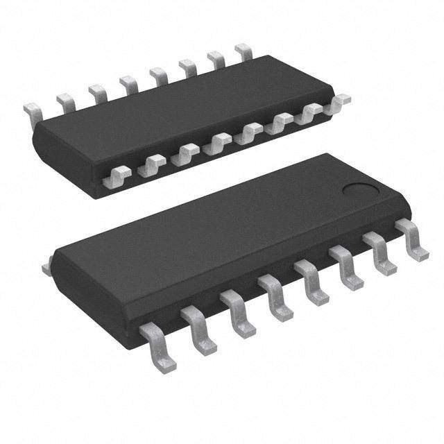
| 描述 | IC SONAR RANGING RCVR 16-SOIC |
| 产品分类 | |
| 品牌 | Texas Instruments |
| 数据手册 | |
| 产品图片 |
|
| 产品型号 | TL852CDR |
| RF类型 | 声纳控制 |
| rohs | 无铅 / 符合限制有害物质指令(RoHS)规范要求 |
| 产品系列 | - |
| 产品培训模块 | http://www.digikey.cn/PTM/IndividualPTM.page?site=cn&lang=zhs&ptm=26085 |
| 产品目录页面 | |
| 供应商器件封装 | 16-SOIC N |
| 其它名称 | 296-17139-6 |
| 制造商产品页 | http://www.ti.com/general/docs/suppproductinfo.tsp?distId=10&orderablePartNumber=TL852CDR |
| 功能 | 声纳测距接收器 |
| 包装 | Digi-Reel® |
| 封装/外壳 | 16-SOIC(0.154",3.90mm 宽) |
| 标准包装 | 1 |
| 辅助属性 | TTL 兼容 |
| 频率 | 20kHz ~ 90kHz |


- 商务部:美国ITC正式对集成电路等产品启动337调查
- 曝三星4nm工艺存在良率问题 高通将骁龙8 Gen1或转产台积电
- 太阳诱电将投资9.5亿元在常州建新厂生产MLCC 预计2023年完工
- 英特尔发布欧洲新工厂建设计划 深化IDM 2.0 战略
- 台积电先进制程称霸业界 有大客户加持明年业绩稳了
- 达到5530亿美元!SIA预计今年全球半导体销售额将创下新高
- 英特尔拟将自动驾驶子公司Mobileye上市 估值或超500亿美元
- 三星加码芯片和SET,合并消费电子和移动部门,撤换高东真等 CEO
- 三星电子宣布重大人事变动 还合并消费电子和移动部门
- 海关总署:前11个月进口集成电路产品价值2.52万亿元 增长14.8%


PDF Datasheet 数据手册内容提取
(cid:1)(cid:2)(cid:3)(cid:4)(cid:5) (cid:6)(cid:7)(cid:8)(cid:9)(cid:10) (cid:10)(cid:9)(cid:8)(cid:11)(cid:12)(cid:8)(cid:11) (cid:10)(cid:13)(cid:14)(cid:13)(cid:12)(cid:15)(cid:13)(cid:10) SLSS003 − SEPTEMBER 1983 − REVISED MARCH 1988 (cid:1) Designed for Use With the TL851 in Sonar N PACKAGE Ranging Modules Like the SN28827 (TOP VIEW) (cid:1) Digitally Controlled Variable-Gain Variable-Bandwidth Amplifier G1IN 1 16 GND (cid:1) XIN 2 15 GCD Operational Frequency Range of 20 kHz GADJ 3 14 GCA to 90 kHz LC 4 13 GCB (cid:1) TTL-Compatible VCC 5 12 GCC (cid:1) Operates From Power Sources of 4.5 V G1OUT 6 11 NC to 6.8 V G2IN 7 10 NC (cid:1) Interfaces to Electrostatic or Piezoelectric BIAS 8 9 REC Transducers (cid:1) Overall Gain Adjustable With One External NC − No internal connection Resistor description The TL852 is an economical sonar ranging receiver integrated circuit for use with the TL851 control integrated circuit. A minimum of external components is required for operation, and this amplifier easily interfaces to Polaroid’s 50-kHz electrostatic transducer. An external 68-kΩ ±5% resistor from BIAS to GND provides the internal biasing reference. Amplifier gain can be set with a resistor from G1IN to GADJ. Required amplifier gain will vary for different applications. Using the detect-level measurement circuit of Figure 1, a nominal peak-to-peak value of 230 mV input during gain step 2 is recommended for most applications. For reliable operation, a level no lower than 50 mV should be used. The recommended detect level of 230 mV can be obtained for most amplifiers with an R1 value between 5 kΩ and 20 kΩ Digital control of amplifier gain is provided with gain control inputs GCA, GCB, GCC, and GCD. These inputs must be driven synchronously (all inputs stable within 0.1 µs) to avoid false receive output signals due to invalid logic counts. This can be done easily with the TL851 control integrated circuit. A plot showing relative gain for the various gain steps versus time can be seen in Figure 2. To dampen ringing of the 50-kHz electrostatic transducer, a 5-kΩ resistor from G1IN to XIN is recommended. An external parallel combination of inductance and capacitance between LC and V provides an amplifier with CC an externally controlled gain and Q. This not only allows control of gain to compensate for attenuation of signal with distance, but also maximizes noise and sidelobe rejection. Care must be taken to accurately tune the L-C combination at operating frequency or gain and Q will be greatly reduced at higher gain steps. AC coupling between stages of the amplifier is accomplished with a 0.01-mF capacitor for proper biasing. The receive output is normally held at a low level by an internal 1-µA current source. When an input of sufficient amplitude is received, the output is driven alternately by the 1-µA discharge current and a 50-µA charging current. A 1000-pF capacitor is required from REC to GND to integrate the received signal so that one or two noise pulses will not be recognized. XIN provides clamping for the transformer secondary when used for transducer transmit drive as shown in Figure 4 of the SN28827 data sheet. The TL852 is characterized for operation from 0°C to 40°C. (cid:16)(cid:10)(cid:7)(cid:17)(cid:18)(cid:14)(cid:1)(cid:12)(cid:7)(cid:8) (cid:17)(cid:9)(cid:1)(cid:9) (cid:19)(cid:20)(cid:21)(cid:22)(cid:23)(cid:24)(cid:25)(cid:26)(cid:19)(cid:22)(cid:20) (cid:19)(cid:27) (cid:28)(cid:29)(cid:23)(cid:23)(cid:30)(cid:20)(cid:26) (cid:25)(cid:27) (cid:22)(cid:21) (cid:31)(cid:29)!"(cid:19)(cid:28)(cid:25)(cid:26)(cid:19)(cid:22)(cid:20) #(cid:25)(cid:26)(cid:30)$ Copyright 1988, Texas Instruments Incorporated (cid:16)(cid:23)(cid:22)#(cid:29)(cid:28)(cid:26)(cid:27) (cid:28)(cid:22)(cid:20)(cid:21)(cid:22)(cid:23)(cid:24) (cid:26)(cid:22) (cid:27)(cid:31)(cid:30)(cid:28)(cid:19)(cid:21)(cid:19)(cid:28)(cid:25)(cid:26)(cid:19)(cid:22)(cid:20)(cid:27) (cid:31)(cid:30)(cid:23) (cid:26)%(cid:30) (cid:26)(cid:30)(cid:23)(cid:24)(cid:27) (cid:22)(cid:21) (cid:1)(cid:30)&(cid:25)(cid:27) (cid:12)(cid:20)(cid:27)(cid:26)(cid:23)(cid:29)(cid:24)(cid:30)(cid:20)(cid:26)(cid:27) (cid:27)(cid:26)(cid:25)(cid:20)#(cid:25)(cid:23)# ’(cid:25)(cid:23)(cid:23)(cid:25)(cid:20)(cid:26)($ (cid:16)(cid:23)(cid:22)#(cid:29)(cid:28)(cid:26)(cid:19)(cid:22)(cid:20) (cid:31)(cid:23)(cid:22)(cid:28)(cid:30)(cid:27)(cid:27)(cid:19)(cid:20)) #(cid:22)(cid:30)(cid:27) (cid:20)(cid:22)(cid:26) (cid:20)(cid:30)(cid:28)(cid:30)(cid:27)(cid:27)(cid:25)(cid:23)(cid:19)"( (cid:19)(cid:20)(cid:28)"(cid:29)#(cid:30) (cid:26)(cid:30)(cid:27)(cid:26)(cid:19)(cid:20)) (cid:22)(cid:21) (cid:25)"" (cid:31)(cid:25)(cid:23)(cid:25)(cid:24)(cid:30)(cid:26)(cid:30)(cid:23)(cid:27)$ POST OFFICE BOX 65•5303 • DALLAS, TEXAS 75265 1 POST OFFICE BOX 1443 HOUSTON, TEXAS 77251−1443
(cid:1)(cid:2)(cid:3)(cid:4)(cid:5) (cid:6)(cid:7)(cid:8)(cid:9)(cid:10) (cid:10)(cid:9)(cid:8)(cid:11)(cid:12)(cid:8)(cid:11) (cid:10)(cid:13)(cid:14)(cid:13)(cid:12)(cid:15)(cid:13)(cid:10) SLSS003 − SEPTEMBER 1983 − REVISED MARCH 1988 functional block diagram 5 VCC 50 µA VCC − 2.1 V 0.3 V 7 G2IN 14 9 GCA REC 13 GCB Gain 12 Control 1 µA GCC 15 GCD Reg Ref 8 BIAS 0.7 V 6 G1OUT 1 G1IN 3 GADJ 4 LC 2 XIN 16 GND schematic of gain control inputs GCA, GCB, GCC, AND GCD VCC INPUT GND 2 POST OFFICE BOX 65•5303 • DALLAS, TEXAS 75265 POST OFFICE BOX 1443 HOUSTON, TEXAS 77251−1443
(cid:1)(cid:2)(cid:3)(cid:4)(cid:5) (cid:6)(cid:7)(cid:8)(cid:9)(cid:10) (cid:10)(cid:9)(cid:8)(cid:11)(cid:12)(cid:8)(cid:11) (cid:10)(cid:13)(cid:14)(cid:13)(cid:12)(cid:15)(cid:13)(cid:10) SLSS003 − SEPTEMBER 1983 − REVISED MARCH 1988 absolute maximum ratings over operating free-air temperature range (unless otherwise noted)† Voltage at any pin with respect to GND . . . . . . . . . . . . . . . . . . . . . . . . . . . . . . . . . . . . . . . . . . . . . . − 0.5 V to 7 V Voltage at any pin with respect to V . . . . . . . . . . . . . . . . . . . . . . . . . . . . . . . . . . . . . . . . . . . . . . . − 7 V to 0.5 V CC XIN input current (50% duty cycle) . . . . . . . . . . . . . . . . . . . . . . . . . . . . . . . . . . . . . . . . . . . . . . . . . . . . . . . . ±60 mA Continuous power dissipation at (or below) 25°C free-air temperature (see Note 1) . . . . . . . . . . . . 1150 mW Operating free-air temperature range . . . . . . . . . . . . . . . . . . . . . . . . . . . . . . . . . . . . . . . . . . . . . . . − 40°C to 85°C Storage temperature range . . . . . . . . . . . . . . . . . . . . . . . . . . . . . . . . . . . . . . . . . . . . . . . . . . . . . . . − 65°C to 150°C Lead temperature 1,6 mm (1/16 inch) from case for 10 seconds . . . . . . . . . . . . . . . . . . . . . . . . . . . . . . . 260°C †Stresses beyond those listed under absolute maximum ratings may cause permanent damage to the device. This is a stress rating only, and functional operation of the device at these or any other conditions beyond those indicated in the recommended operating conditions section of this specification is not implied. Exposure to absolute-maximum-rated conditions for extended periods may affect device reliability. NOTE 1: For operation above 25°C, derate linearly at the rate of 9.2 mW/°C. recommended operating conditions MIN MAX UNIT Supply voltage, VCC 4.5 6.8 V High-level input voltage, VIH 2.1 GGCCAA,, GGCCBB,, GGCCCC,, GGCCDD VV Low-level input voltage, VIL 0.6 Bias resistor between BIAS and GND 64 72 kΩ Operating free-air temperature, TA 0 40 °C electrical characteristics over recommended ranges of supply voltage and operating free-air temperature (unless otherwise noted) PARAMETER TEST CONDITIONS MIN TYP‡ MAX UNIT II = 40 mA 2.5 IInnppuutt ccllaammpp vvoollttaaggee aatt XXIINN VV II = − 40 mA − 1.5 Open-circuit input voltage at GCA, GCB, GCC, GCD VCC = 5 V, II = 0 2.5 V High-level input current, IIH, into GCA, GCB, GCC, GCD VCC = 5 V, VIH = 2 V − 0.5 mA Low-level input current, IIL, into GCA, GCB, GCC, GCD VCC = 5 V, VIL = 0 − 3 mA IG2IN = − 100 µA, VO = 0.3 V 1 RRaacceeiivvee oouuttppuutt ccuurrrreenntt µAA IG2IN = 100 µA, VO = 0.1 V − 50 Supply current, ICC 45 mA ‡Typical values are at VCC = 5 V and TA = 25°C. POST OFFICE BOX 65•5303 • DALLAS, TEXAS 75265 3 POST OFFICE BOX 1443 HOUSTON, TEXAS 77251−1443
(cid:1)(cid:2)(cid:3)(cid:4)(cid:5) (cid:6)(cid:7)(cid:8)(cid:9)(cid:10) (cid:10)(cid:9)(cid:8)(cid:11)(cid:12)(cid:8)(cid:11) (cid:10)(cid:13)(cid:14)(cid:13)(cid:12)(cid:15)(cid:13)(cid:10) SLSS003 − SEPTEMBER 1983 − REVISED MARCH 1988 APPLICATION INFORMATION detect level versus gain step Detect level is measured by applying a 15-cycle burst of 49.4 kHz square wave just after the beginning of the gain step to be tested. The least burst amplitude that makes REC reach the trip level is defined to be the detect level. System gain is then inversely proportional to detect level. See the test circuit in Figure 1. VCC 68 kΩ TL331 8 9 Trip Detect BIAS REC Level L1 7 10 G2IN NC 1000 pF 1 mH 0.01 µF 6 NC 11 G1OUT 12 15-Cycle 5 GCC 49.4-kHz VCC 13 Variable-Amplitude 0.01 µF 4 GCB Burst Generator R1 3 LC GCA 14 490 kΩ 21 mH 5 kΩ 2 GADJ GCD 15 XIN 16 0.0022 µF 1 G1IN GND 5 kΩ 500 pF All Resistors ±1%, 1/4 W All Capacitors ±1%, Film L1 Q > 60 at 50 kHz C1 Q > 500 at 50 kHz 15 Pulses Input Signal Trip Level Rec Output Comparator Output Figure 1. Detect-Level Measurement Circuit and Waveforms 4 POST OFFICE BOX 65•5303 • DALLAS, TEXAS 75265 POST OFFICE BOX 1443 HOUSTON, TEXAS 77251−1443
(cid:1)(cid:2)(cid:3)(cid:4)(cid:5) (cid:6)(cid:7)(cid:8)(cid:9)(cid:10) (cid:10)(cid:9)(cid:8)(cid:11)(cid:12)(cid:8)(cid:11) (cid:10)(cid:13)(cid:14)(cid:13)(cid:12)(cid:15)(cid:13)(cid:10) SLSS003 − SEPTEMBER 1983 − REVISED MARCH 1988 APPLICATION INFORMATION GAIN STEP TABLE STEP GCD GCC GCB GCA NUMBER L L L L 0 L L L H 1 L L H L 2 L L H H 3 L H L L 4 L H L H 5 L H H L 6 L H H H 7 H L L L 8 H L L H 9 H L H L 10 H L H H 11 Receiver Gain vs Gain Step Numbers 100 70 40 20 n ai G r 10 e 7 v ei c 4 e R ve 2 ati el R 1 0.7 0.4 0.2 0.1 0 1 2 3 4 5 6 7 8 9 10 11 Gain Steps Figure 2 POST OFFICE BOX 65•5303 • DALLAS, TEXAS 75265 5 POST OFFICE BOX 1443 HOUSTON, TEXAS 77251−1443
PACKAGE OPTION ADDENDUM www.ti.com 6-Feb-2020 PACKAGING INFORMATION Orderable Device Status Package Type Package Pins Package Eco Plan Lead/Ball Finish MSL Peak Temp Op Temp (°C) Device Marking Samples (1) Drawing Qty (2) (6) (3) (4/5) TL852CDR ACTIVE SOIC D 16 2500 Green (RoHS NIPDAU Level-1-260C-UNLIM TL852C & no Sb/Br) TL852CN ACTIVE PDIP N 16 25 Green (RoHS NIPDAU N / A for Pkg Type TL852CN & no Sb/Br) TL852CN ACTIVE PDIP N 16 25 Green (RoHS NIPDAU N / A for Pkg Type TL852CN & no Sb/Br) TL852CNE4 ACTIVE PDIP N 16 25 Green (RoHS NIPDAU N / A for Pkg Type TL852CN & no Sb/Br) TL852CNE4 ACTIVE PDIP N 16 25 Green (RoHS NIPDAU N / A for Pkg Type TL852CN & no Sb/Br) (1) The marketing status values are defined as follows: ACTIVE: Product device recommended for new designs. LIFEBUY: TI has announced that the device will be discontinued, and a lifetime-buy period is in effect. NRND: Not recommended for new designs. Device is in production to support existing customers, but TI does not recommend using this part in a new design. PREVIEW: Device has been announced but is not in production. Samples may or may not be available. OBSOLETE: TI has discontinued the production of the device. (2) RoHS: TI defines "RoHS" to mean semiconductor products that are compliant with the current EU RoHS requirements for all 10 RoHS substances, including the requirement that RoHS substance do not exceed 0.1% by weight in homogeneous materials. Where designed to be soldered at high temperatures, "RoHS" products are suitable for use in specified lead-free processes. TI may reference these types of products as "Pb-Free". RoHS Exempt: TI defines "RoHS Exempt" to mean products that contain lead but are compliant with EU RoHS pursuant to a specific EU RoHS exemption. Green: TI defines "Green" to mean the content of Chlorine (Cl) and Bromine (Br) based flame retardants meet JS709B low halogen requirements of <=1000ppm threshold. Antimony trioxide based flame retardants must also meet the <=1000ppm threshold requirement. (3) MSL, Peak Temp. - The Moisture Sensitivity Level rating according to the JEDEC industry standard classifications, and peak solder temperature. (4) There may be additional marking, which relates to the logo, the lot trace code information, or the environmental category on the device. (5) Multiple Device Markings will be inside parentheses. Only one Device Marking contained in parentheses and separated by a "~" will appear on a device. If a line is indented then it is a continuation of the previous line and the two combined represent the entire Device Marking for that device. (6) Lead/Ball Finish - Orderable Devices may have multiple material finish options. Finish options are separated by a vertical ruled line. Lead/Ball Finish values may wrap to two lines if the finish value exceeds the maximum column width. Addendum-Page 1
PACKAGE OPTION ADDENDUM www.ti.com 6-Feb-2020 Important Information and Disclaimer:The information provided on this page represents TI's knowledge and belief as of the date that it is provided. TI bases its knowledge and belief on information provided by third parties, and makes no representation or warranty as to the accuracy of such information. Efforts are underway to better integrate information from third parties. TI has taken and continues to take reasonable steps to provide representative and accurate information but may not have conducted destructive testing or chemical analysis on incoming materials and chemicals. TI and TI suppliers consider certain information to be proprietary, and thus CAS numbers and other limited information may not be available for release. In no event shall TI's liability arising out of such information exceed the total purchase price of the TI part(s) at issue in this document sold by TI to Customer on an annual basis. Addendum-Page 2
PACKAGE MATERIALS INFORMATION www.ti.com 26-Feb-2019 TAPE AND REEL INFORMATION *Alldimensionsarenominal Device Package Package Pins SPQ Reel Reel A0 B0 K0 P1 W Pin1 Type Drawing Diameter Width (mm) (mm) (mm) (mm) (mm) Quadrant (mm) W1(mm) TL852CDR SOIC D 16 2500 330.0 16.4 6.5 10.3 2.1 8.0 16.0 Q1 PackMaterials-Page1
PACKAGE MATERIALS INFORMATION www.ti.com 26-Feb-2019 *Alldimensionsarenominal Device PackageType PackageDrawing Pins SPQ Length(mm) Width(mm) Height(mm) TL852CDR SOIC D 16 2500 350.0 350.0 43.0 PackMaterials-Page2
None
None
None
IMPORTANTNOTICEANDDISCLAIMER TI PROVIDES TECHNICAL AND RELIABILITY DATA (INCLUDING DATASHEETS), DESIGN RESOURCES (INCLUDING REFERENCE DESIGNS), APPLICATION OR OTHER DESIGN ADVICE, WEB TOOLS, SAFETY INFORMATION, AND OTHER RESOURCES “AS IS” AND WITH ALL FAULTS, AND DISCLAIMS ALL WARRANTIES, EXPRESS AND IMPLIED, INCLUDING WITHOUT LIMITATION ANY IMPLIED WARRANTIES OF MERCHANTABILITY, FITNESS FOR A PARTICULAR PURPOSE OR NON-INFRINGEMENT OF THIRD PARTY INTELLECTUAL PROPERTY RIGHTS. These resources are intended for skilled developers designing with TI products. You are solely responsible for (1) selecting the appropriate TI products for your application, (2) designing, validating and testing your application, and (3) ensuring your application meets applicable standards, and any other safety, security, or other requirements. These resources are subject to change without notice. TI grants you permission to use these resources only for development of an application that uses the TI products described in the resource. Other reproduction and display of these resources is prohibited. No license is granted to any other TI intellectual property right or to any third party intellectual property right. TI disclaims responsibility for, and you will fully indemnify TI and its representatives against, any claims, damages, costs, losses, and liabilities arising out of your use of these resources. TI’s products are provided subject to TI’s Terms of Sale (www.ti.com/legal/termsofsale.html) or other applicable terms available either on ti.com or provided in conjunction with such TI products. TI’s provision of these resources does not expand or otherwise alter TI’s applicable warranties or warranty disclaimers for TI products. Mailing Address: Texas Instruments, Post Office Box 655303, Dallas, Texas 75265 Copyright © 2020, Texas Instruments Incorporated