ICGOO在线商城 > 射频/IF 和 RFID > RF 其它 IC 和模块 > AD6642BBCZ
 Datasheet下载
- 型号: AD6642BBCZ
- 制造商: Analog
- 库位|库存: xxxx|xxxx
- 要求:
| 数量阶梯 | 香港交货 | 国内含税 |
| +xxxx | $xxxx | ¥xxxx |
查看当月历史价格
查看今年历史价格
AD6642BBCZ产品简介:
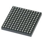
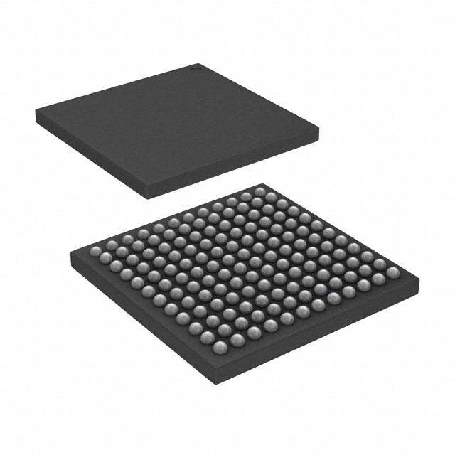
ICGOO电子元器件商城为您提供AD6642BBCZ由Analog设计生产,在icgoo商城现货销售,并且可以通过原厂、代理商等渠道进行代购。 AD6642BBCZ价格参考。AnalogAD6642BBCZ封装/规格:RF 其它 IC 和模块, RF IC IF Receiver CDMA, LTE, W-CDMA, WiMAX Sample Rates to 200MSPS 144-CSBGA (10x10)。您可以下载AD6642BBCZ参考资料、Datasheet数据手册功能说明书,资料中有AD6642BBCZ 详细功能的应用电路图电压和使用方法及教程。
AD6642BBCZ 是 Analog Devices Inc.(亚德诺半导体公司)推出的一款高性能射频(RF)直接转换接收器芯片,广泛应用于通信系统中。它主要面向无线基础设施、软件定义无线电(SDR)、测试设备及工业控制系统等场景。

该芯片集成了两个14位、125 MSPS模数转换器(ADC),支持宽带信号采集和处理,具备良好的动态性能和低功耗特性。其典型应用场景包括:

1. 无线基站接收端:用于4G/5G通信系统中的中频或直接射频采样接收链路,实现高精度信号数字化;
2. 软件无线电平台:作为核心数据采集模块,支持多频段、多标准通信协议的灵活配置;
3. 测试与测量设备:如频谱分析仪、信号分析仪等,提供高分辨率和宽动态范围以精确捕捉复杂信号;
4. 雷达与电子战系统:用于信号侦测、识别与分析,满足对高频信号的实时处理需求;
5. 工业控制与监测系统:在远程监控、传感器网络中实现高速模拟信号到数字信号的转换。

AD6642BBCZ 采用先进的CMOS工艺制造,具备良好的集成度和稳定性,适合高性能、低延迟的射频信号处理应用。
| 参数 | 数值 |
| 产品目录 | |
| 描述 | IC IF RCVR 11BIT 200MSPS 144BGA模数转换器 - ADC IC 11B Dual IF Diversity Receiver |
| DevelopmentKit | AD6642EBZ |
| 产品分类 | |
| 品牌 | Analog Devices |
| 产品手册 | |
| 产品图片 |
|
| rohs | 符合RoHS无铅 / 符合限制有害物质指令(RoHS)规范要求 |
| 产品系列 | 数据转换器IC,模数转换器 - ADC,Analog Devices AD6642BBCZ- |
| 数据手册 | |
| 产品型号 | AD6642BBCZ |
| RF类型 | CDMA,LTE,W-CDMA,WiMAX |
| 产品种类 | 模数转换器 - ADC |
| 供应商器件封装 | 144-CSBGA(10x10) |
| 信噪比 | 75.5 dB |
| 分辨率 | 11 bit |
| 功能 | IF 接收器 |
| 包装 | 托盘 |
| 商标 | Analog Devices |
| 安装风格 | SMD/SMT |
| 封装 | Tray |
| 封装/外壳 | 144-LFBGA,CSPBGA |
| 封装/箱体 | CSPBGA-144 |
| 工作电源电压 | 1.7 V to 1.9 V |
| 工厂包装数量 | 184 |
| 接口类型 | LVDS, SPI |
| 最大功率耗散 | 620 mW |
| 最大工作温度 | + 85 C |
| 最小工作温度 | - 40 C |
| 标准包装 | 1 |
| 电压参考 | Internal |
| 系列 | AD6642 |
| 结构 | Pipeline |
| 视频文件 | http://www.digikey.cn/classic/video.aspx?PlayerID=1364138032001&width=640&height=505&videoID=2245193150001 |
| 转换器数量 | 2 |
| 转换速率 | 200 MS/s |
| 辅助属性 | 采样率达 200MSPS |
| 输入类型 | Single-Ended/Differential |
| 通道数量 | 2 Channel |
| 频率 | - |


- 商务部:美国ITC正式对集成电路等产品启动337调查
- 曝三星4nm工艺存在良率问题 高通将骁龙8 Gen1或转产台积电
- 太阳诱电将投资9.5亿元在常州建新厂生产MLCC 预计2023年完工
- 英特尔发布欧洲新工厂建设计划 深化IDM 2.0 战略
- 台积电先进制程称霸业界 有大客户加持明年业绩稳了
- 达到5530亿美元!SIA预计今年全球半导体销售额将创下新高
- 英特尔拟将自动驾驶子公司Mobileye上市 估值或超500亿美元
- 三星加码芯片和SET,合并消费电子和移动部门,撤换高东真等 CEO
- 三星电子宣布重大人事变动 还合并消费电子和移动部门
- 海关总署:前11个月进口集成电路产品价值2.52万亿元 增长14.8%


PDF Datasheet 数据手册内容提取
Dual IF Receiver AD6642 FEATURES FUNCTIONAL BLOCK DIAGRAM 11-bit, 200 MSPS output data rate per channel AVDD AGND DRVDD DRGND Integrated noise shaping requantizer (NSR) Performance with NSR enabled AD6642 DC0±AB SNR: 75.5 dBFS in 40 MHz band to 70 MHz @ 185 MSPS VIN+A PIPELINE 14 NOISE SHAPING 11 XERERS D0±AB PeSrfNoRrm: 7a3n.7ce d wBFitSh iNn S6R0 dMisHazb bleadn d to 70 MHz @ 185 MSPS VVICNM–AA ADC REQUANTIZER LTIPLES DRIV SSNFDRR: 6: 863.5 d dBBcF tSo t 7o0 7 M0 HMzH @z @18 158 M5 SMPSSP S VVIINN+–BB PIPAEDLCINE 14 NROEIQSEU ASNHTAIPZIENRG 11 DATA MUANDLVD D10±AB VCMB Low power: 0.62 W @ 185 MSPS MODE REFERENCE 1.8 V analog supply operation CLOCK SYNC 1.8 V LVDS (ANSI-644 levels) output DIVIDER 1-to-8 integer clock divider SERIAL PORT PDWN I1n.7te5r Vna pl -ApD aCn avloolgta ignep uretf rearnegnece (p rogrammable to 2.0 V p-p) SCLK SDIO CSB CLK+ CLK– 08563-001 Differential analog inputs with 800 MHz bandwidth Figure 1. 95 dB channel isolation/crosstalk PRODUCT HIGHLIGHTS Serial port control User-configurable built-in self-test (BIST) capability 1. Two ADCs are contained in a small, space-saving, Energy-saving power-down modes 10 mm × 10 mm × 1.4 mm, 144-ball CSP_BGA package. 2. Pin selectable noise shaping requantizer (NSR) function APPLICATIONS that allows for improved SNR within a reduced bandwidth Communications of up to 60 MHz at 185 MSPS. Diversity radio and smart antenna (MIMO) systems 3. LVDS digital output interface configured for low cost Multimode digital receivers (3G) FPGA families. WCDMA, LTE, CDMA2000 4. 120 mW per ADC core power consumption. WiMAX, TD-SCDMA 5. Operation from a single 1.8 V supply. I/Q demodulation systems 6. Standard serial port interface (SPI) that supports various General-purpose software radios product features and functions, such as data formatting (offset binary or twos complement), NSR, power-down, test modes, and voltage reference mode. 7. On-chip integer 1-to-8 input clock divider and multichip sync function to support a wide range of clocking schemes and multichannel subsystems. Rev. A Information furnished by Analog Devices is believed to be accurate and reliable. However, no responsibility is assumed by Analog Devices for its use, nor for any infringements of patents or other One Technology Way, P.O. Box 9106, Norwood, MA 02062-9106, U.S.A. rights of third parties that may result from its use. Specifications subject to change without notice. No license is granted by implication or otherwise under any patent or patent rights of Analog Devices. Tel: 781.329.4700 www.analog.com Trademarks and registered trademarks are the property of their respective owners. Fax: 781.461.3113 ©2009–2010 Analog Devices, Inc. All rights reserved.
AD6642 TABLE OF CONTENTS Features..............................................................................................1 Power Dissipation and Standby Mode....................................20 Applications.......................................................................................1 Channel/Chip Synchronization................................................20 Functional Block Diagram..............................................................1 Digital Outputs...........................................................................21 Product Highlights...........................................................................1 Timing.........................................................................................21 Revision History...............................................................................2 Noise Shaping Requantizer (NSR)...............................................22 General Description.........................................................................3 22% BW Mode (>40 MHz @ 184.32 MSPS)...........................22 Specifications.....................................................................................4 33% BW Mode (>60 MHz @ 184.32 MSPS)...........................22 DC Specifications.........................................................................4 MODE Pin...................................................................................23 AC Specifications..........................................................................5 Built-In Self-Test (BIST) and Output Test..................................24 Digital Specifications...................................................................6 Built-In Self-Test (BIST)............................................................24 Switching Specifications..............................................................7 Output Test Modes.....................................................................24 Timing Specifications..................................................................8 Serial Port Interface (SPI)..............................................................25 Absolute Maximum Ratings............................................................9 Configuration Using the SPI.....................................................25 Thermal Characteristics..............................................................9 Hardware Interface.....................................................................25 ESD Caution..................................................................................9 Memory Map..................................................................................26 Pin Configuration and Function Descriptions...........................10 Reading the Memory Map Register Table...............................26 Typical Performance Characteristics...........................................12 Memory Map Register Table.....................................................27 Equivalent Circuits.........................................................................15 Memory Map Register Descriptions........................................29 Theory of Operation......................................................................16 Applications Information..............................................................30 ADC Architecture......................................................................16 Design Guidelines......................................................................30 Analog Input Considerations....................................................16 Outline Dimensions.......................................................................31 Clock Input Considerations......................................................18 Ordering Guide..........................................................................31 REVISION HISTORY 7/10—Rev. 0 to Rev. A Changes to ADC Architecture Section........................................16 Changes to Figure 34 and Figure 35.............................................18 Changes to Timing Section and Data Clock Output (DCO) Section..............................................................................................21 Changes to 22% BW Mode (>40 MHz @ 184.32 MSPS) Section and 33% BW Mode (>60 MHz @ 184.32 MSPS) Section .........22 Changes to Design Guidelines Section........................................30 10/09—Revision 0: Initial Version Rev. A | Page 2 of 32
AD6642 GENERAL DESCRIPTION The AD6642 is an 11-bit, 200 MSPS, dual-channel intermediate With the NSR block disabled, the ADC data is provided directly to frequency (IF) receiver specifically designed to support multi- the output with a resolution of 11 bits. The AD6642 can achieve antenna systems in telecommunication applications where high up to 66.5 dBFS SNR for the entire Nyquist bandwidth when dynamic range performance, low power, and small size are desired. operated in this mode. This allows the AD6642 to be used in telecommunication applications such as a digital predistortion The device consists of two high performance analog-to-digital observation path where wider bandwidths are desired. converters (ADCs) and noise shaping requantizer (NSR) digital blocks. Each ADC consists of a multistage, differential pipelined After digital signal processing, multiplexed output data is architecture with integrated output error correction logic. The routed into two 11-bit output ports such that the maximum ADC features a wide bandwidth switched-capacitor sampling data rate is 400 Mbps (DDR). These outputs are set at 1.8 V network within the first stage of the differential pipeline. An LVDS and support ANSI-644 levels. integrated voltage reference eases design considerations. A duty The AD6642 receiver digitizes a wide spectrum of IF frequencies. cycle stabilizer (DCS) compensates for variations in the ADC Each receiver is designed for simultaneous reception of a separate clock duty cycle, allowing the converters to maintain excellent antenna. This IF sampling architecture greatly reduces compo- performance. nent cost and complexity compared with traditional analog Each ADC output is connected internally to an NSR block. The techniques or less integrated digital methods. integrated NSR circuitry allows for improved SNR performance Flexible power-down options allow significant power savings. in a smaller frequency band within the Nyquist bandwidth. The Programming for device setup and control is accomplished device supports two different output modes selectable via the using a 3-wire SPI-compatible serial interface with numerous external MODE pin or the SPI. modes to support board-level system testing. With the NSR feature enabled, the outputs of the ADCs are The AD6642 is available in a Pb-free/RoHS compliant, 144-ball, processed such that the AD6642 supports enhanced SNR 10 mm × 10 mm chip scale package ball grid array (CSP_BGA) performance within a limited portion of the Nyquist bandwidth and is specified over the industrial temperature range of −40°C while maintaining an 11-bit output resolution. The NSR block to +85°C. can be programmed to provide a bandwidth of either 22% or 33% of the sample clock. For example, with a sample clock rate of 185 MSPS, the AD6642 can achieve up to 75.5 dBFS SNR for a 40 MHz bandwidth in the 22% mode and up to 73.7 dBFS SNR for a 60 MHz bandwidth in the 33% mode. Rev. A | Page 3 of 32
AD6642 SPECIFICATIONS DC SPECIFICATIONS AVDD = 1.8 V, DRVDD = 1.8 V, f = 185 MSPS, 1.75 V p-p differential input, VIN = −1.0 dBFS differential input, and default SPI, unless S otherwise noted. Table 1. Parameter Temperature Min Typ Max Unit RESOLUTION Full 11 Bits ACCURACY No Missing Codes Full Guaranteed Offset Error Full −4.5 2 7.4 mV Gain Error Full ±3 ±7 % FSR Differential Nonlinearity (DNL)1 Full ±0.1 ±0.5 LSB Integral Nonlinearity (INL)1 Full ±0.2 ±0.5 LSB MATCHING CHARACTERISTIC Offset Error Full −2.4 2.5 8.3 mV Gain Error Full ±1 ±3 % FSR TEMPERATURE DRIFT Offset Error Full 2 ppm/°C Gain Error Full 40 ppm/°C ANALOG INPUT Input Range Full 1.4 1.75 2.0 V p-p Input Common-Mode Voltage Full 0.9 V Input Resistance (Differential) Full 20 kΩ Input Capacitance2 Full 5 pF POWER SUPPLIES Supply Voltage AVDD Full 1.7 1.8 1.9 V DRVDD Full 1.7 1.8 1.9 V Supply Current I 1 Full 265 291 mA AVDD I 1 (1.8 V LVDS) Full 79 89 mA DRVDD POWER CONSUMPTION Sine Wave Input1 Full 619 684 mW Standby Power3 Full 83 mW Power-Down Power Full 4.5 18 mW 1 Measured with a 10 MHz, 0 dBFS sine wave, with 100 Ω termination on each LVDS output pair. 2 Input capacitance refers to the effective capacitance between one differential input pin and AGND. 3 Standby power is measured with a dc input and the CLKx pins inactive (set to AVDD or AGND). Rev. A | Page 4 of 32
AD6642 AC SPECIFICATIONS AVDD = 1.8 V, DRVDD = 1.8 V, f = 185 MSPS, 1.75 V p-p differential input, VIN = −1.0 dBFS differential input, and default SPI, unless S otherwise noted. Table 2. Parameter1 Temperature Min Typ Max Unit SIGNAL-TO-NOISE-RATIO (SNR)—NSR DISABLED f = 30 MHz 25°C 66.5 dBFS IN f = 70 MHz 25°C 66.5 dBFS IN f = 170 MHz Full 65.7 66.1 dBFS IN f = 250 MHz 25°C 65.5 dBFS IN SIGNAL-TO-NOISE-RATIO (SNR)—NSR ENABLED 22% BW Mode f = 70 MHz 25°C 75.5 dBFS IN f = 170 MHz Full 72.8 74.4 dBFS IN f = 230 MHz 25°C 72.8 dBFS IN 33% BW Mode f = 70 MHz 25°C 73.7 dBFS IN f = 170 MHz Full 71.0 72.6 dBFS IN f = 230 MHz 25°C 71.0 dBFS IN SIGNAL-TO-NOISE-AND DISTORTION (SINAD) f = 30 MHz 25°C 65.5 dBFS IN f = 70 MHz 25°C 66.3 dBFS IN f = 170 MHz Full 64.1 65.6 dBFS IN f = 250 MHz 25°C 64.3 dBFS IN EFFECTIVE NUMBER OF BITS (ENOB) f = 30 MHz 25°C 10.6 Bits IN f = 70 MHz 25°C 10.7 Bits IN f = 170 MHz Full 10.3 10.6 Bits IN f = 250 MHz 25°C 10.3 Bits IN WORST SECOND OR THIRD HARMONIC f = 30 MHz 25°C −90 dBc IN f = 70 MHz 25°C −83 dBc IN f = 170 MHz Full −72 −78 dBc IN f = 250 MHz 25°C −80 dBc IN SPURIOUS-FREE DYNAMIC RANGE (SFDR) f = 30 MHz 25°C 90 dBc IN f = 70 MHz 25°C 83 dBc IN f = 170 MHz Full 72 78 dBc IN f = 250 MHz 25°C 80 dBc IN WORST OTHER HARMONIC (FOURTH THROUGH EIGHTH) f = 30 MHz 25°C −100 dBc IN f = 70 MHz 25°C −96 dBc IN f = 170 MHz Full −82 −90 dBc IN f = 250 MHz 25°C −95 dBc IN TWO-TONE SFDR (−7 dBFS) f = 169 MHz, f = 172 MHz 25°C 82 dBc IN1 IN2 CROSSTALK2 Full 95 dB ANALOG INPUT BANDWIDTH 25°C 800 MHz 1 See the AN-835 Application Note, Understanding High Speed ADC Testing and Evaluation, for a complete set of definitions. 2 Crosstalk is measured at 155 MHz with −1 dBFS on one channel and no input on the alternate channel. Rev. A | Page 5 of 32
AD6642 DIGITAL SPECIFICATIONS AVDD = 1.8 V, DRVDD = 1.8 V, f = 185 MSPS, 1.75 V p-p differential input, VIN = −1.0 dBFS differential input, and default SPI, unless S otherwise noted. Table 3. Parameter Temperature Min Typ Max Unit DIFFERENTIAL CLOCK INPUTS (CLK+, CLK−) Logic Compliance CMOS/LVDS/LVPECL Internal Common-Mode Bias Full 0.9 V Differential Input Voltage Full 0.2 3.6 V p-p Input Voltage Range Full AGND − 0.3 AVDD + 0.2 V High Level Input Voltage Full 1.2 2.0 V Low Level Input Voltage Full 0 0.8 V High Level Input Current Full −10 +10 μA Low Level Input Current Full −10 +10 μA Input Resistance Full 8 10 12 kΩ Input Capacitance Full 4 pF SYNC INPUT Logic Compliance CMOS Internal Bias Full 0.9 V Input Voltage Range Full AGND AVDD V High Level Input Voltage Full 1.2 AVDD V Low Level Input Voltage Full AGND 0.6 V High Level Input Current Full −100 +100 μA Low Level Input Current Full −100 +100 μA Input Resistance Full 12 16 20 kΩ Input Capacitance Full 1 pF LOGIC INPUT (CSB)1 High Level Input Voltage Full 1.22 2.1 V Low Level Input Voltage Full 0 0.6 V High Level Input Current Full −10 +10 μA Low Level Input Current Full 40 132 μA Input Resistance Full 26 kΩ Input Capacitance Full 2 pF LOGIC INPUT (SCLK)2 High Level Input Voltage Full 1.22 2.1 V Low Level Input Voltage Full 0 0.6 V High Level Input Current Full −92 −135 μA Low Level Input Current Full −10 +10 μA Input Resistance Full 26 kΩ Input Capacitance Full 2 pF LOGIC INPUT/OUTPUT (SDIO)2 High Level Input Voltage Full 1.22 2.1 V Low Level Input Voltage Full 0 0.6 V High Level Input Current Full −10 +10 μA Low Level Input Current Full 38 128 μA Input Resistance Full 26 kΩ Input Capacitance Full 5 pF LOGIC INPUT (MODE)1 High Level Input Voltage Full 1.22 2.1 V Low Level Input Voltage Full 0 0.6 V High Level Input Current Full −10 +10 μA Low Level Input Current Full 40 132 μA Rev. A | Page 6 of 32
AD6642 Parameter Temperature Min Typ Max Unit Input Resistance Full 26 kΩ Input Capacitance Full 2 pF LOGIC INPUT (PDWN)2 High Level Input Voltage Full 1.22 2.1 V Low Level Input Voltage Full 0 0.6 V High Level Input Current Full −90 −134 μA Low Level Input Current Full −10 +10 μA Input Resistance Full 26 kΩ Input Capacitance Full 5 pF DIGITAL OUTPUTS (LVDS) Differential Output Voltage (V ) Full 247 454 mV OD Output Offset Voltage (V ) Full 1.125 1.375 V OS 1 Pull up. 2 Pull down. SWITCHING SPECIFICATIONS AVDD = 1.8 V, DRVDD = 1.8 V, f = 185 MSPS, 1.75 V p-p differential input, VIN = −1.0 dBFS differential input, and default SPI, unless S otherwise noted. Table 4. Parameter Temperature Min Typ Max Unit CLOCK INPUT PARAMETERS Input Clock Rate Full 625 MHz Conversion Rate1 Full 40 185 200 MSPS CLK Pulse Width High (t ) Full 2.7 ns CH Aperture Delay (t ) Full 1.3 ns A Aperture Uncertainty (Jitter, t) Full 0.13 ps rms J DATA OUTPUT PARAMETERS Data Propagation Delay (t ) Full 3.0 4.35 5.7 ns PD DCO Propagation Delay (t ) Full 3.2 4.55 5.9 ns DCO DCO to Data Skew (t ) Full −0.4 −0.2 0 ns SKEW Pipeline Delay (Latency) Full 9 Cycles With NSR Enabled Full 12 Cycles Wake-Up Time2 Full 1.2 μs OUT-OF-RANGE RECOVERY TIME Full 2 Cycles 1 Conversion rate is the clock rate after the divider. 2 Wake-up time is dependent on the value of the decoupling capacitors. Rev. A | Page 7 of 32
AD6642 TIMING SPECIFICATIONS AVDD = 1.8 V, DRVDD = 1.8 V, f = 185 MSPS, 1.75 V p-p differential input, VIN = −1.0 dBFS differential input, and default SPI, unless S otherwise noted. Table 5. Parameter Description Min Typ Max Unit SYNC TIMING REQUIREMENTS t SYNC to rising edge of CLK setup time 0.24 ns SSYNC t SYNC to rising edge of CLK hold time 0.40 ns HSYNC SPI TIMING REQUIREMENTS t Setup time between the data and the rising edge of SCLK 2 ns DS t Hold time between the data and the rising edge of SCLK 2 ns DH t Period of the SCLK 40 ns CLK t Setup time between CSB and SCLK 2 ns S t Hold time between CSB and SCLK 2 ns H t SCLK pulse width high 10 ns HIGH t SCLK pulse width low 10 ns LOW t Time required for the SDIO pin to switch from an input to 10 ns EN_SDIO an output relative to the SCLK falling edge t Time required for the SDIO pin to switch from an output to 10 ns DIS_SDIO an input relative to the SCLK rising edge Timing Diagrams N – 1 tA N + 4 N + 5 N N + 3 VIN N + 1 N + 2 t CH tCL 1/fS CLK+ CLK– t DCO DCO+ DCO– t SKEW t PD D10+AB (MSB) D10A D10B D10A D10B D10A D10B D10A D10B D10A D10B D10A D10B D10A D10B D10–AB (MSB) D0+AB (LSB) D0–AB (LSB) D0A D0B D0A D0B D0A D0B D0A D0B D0A D0B D0A D0B D0A D0B 08563-002 Figure 2. Data Output Timing CLK+ t t SSYNC HSYNC SYNC 08563-003 Figure 3. SYNC Input Timing Requirements Rev. A | Page 8 of 32
AD6642 ABSOLUTE MAXIMUM RATINGS THERMAL CHARACTERISTICS Table 6. Parameter Rating The values in Table 7 are per JEDEC JESD51-7 plus JEDEC AVDD to AGND −0.3 V to +2.0 V JESD25-5 for a 2S2P test board. Typical θJA is specified for a DRVDD to AGND −0.3 V to +2.0 V 4-layer PCB with a solid ground plane. As shown in Table 7, VIN+x, VIN−x to AGND −0.3 V to AVDD + 0.2 V airflow improves heat dissipation, which reduces θJA. In addi- CLK+, CLK− to AGND −0.3 V to AVDD + 0.2 V tion, metal in direct contact with the package leads from metal SYNC to AGND −0.3 V to AVDD + 0.2 V traces, through holes, ground, and power planes reduces θJA. VCMx to AGND −0.3 V to AVDD + 0.2 V Table 7. CSB to AGND −0.3 V to DRVDD + 0.2 V Airflow SCLK to AGND −0.3 V to DRVDD + 0.2 V Package Type Velocity θ 1 θ 2 θ 3 Unit JA JC JB SDIO to AGND −0.3 V to DRVDD + 0.2 V 144-Ball CSP_BGA, 0 m/s 26.9 8.9 6.6 °C/W PDWN to AGND −0.3 V to DRVDD + 0.2 V 10 mm × 10 mm 1 m/s 24.2 MODE to AGND −0.3 V to DRVDD + 0.2 V (BC-144-1) 2.5 m/s 23.0 Digital Outputs to AGND −0.3 V to DRVDD + 0.2 V DCO+AB, DCO−AB to AGND −0.3 V to DRVDD + 0.2 V 1 Per JEDEC JESD51-2 (still air) or JEDEC JESD51-6 (moving air). 2 Per MIL-STD 883, Method 1012.1. Operating Temperature Range −40°C to +85°C 3 Per JEDEC JESD51-8 (still air). (Ambient) Maximum Junction Temperature 150°C The values in Table 8 are from simulations. The PCB is a JEDEC Under Bias multilayer board. Thermal performance for actual applications Storage Temperature Range −65°C to +150°C requires careful inspection of the conditions in the application (Ambient) to determine whether they are similar to those assumed in these calculations. Stresses above those listed under Absolute Maximum Ratings may cause permanent damage to the device. This is a stress Table 8. rating only; functional operation of the device at these or any Airflow other conditions above those indicated in the operational Package Type Velocity ΨJB ΨJT Unit section of this specification is not implied. Exposure to absolute 144-Ball CSP_BGA, 0 m/s 14.4 0.23 °C/W maximum rating conditions for extended periods may affect 10 mm × 10 mm 1 m/s 14.0 0.50 (BC-144-1) device reliability. 2.5 m/s 13.9 0.53 ESD CAUTION Rev. A | Page 9 of 32
AD6642 PIN CONFIGURATION AND FUNCTION DESCRIPTIONS 1 2 3 4 5 6 7 8 9 10 11 12 A AGND DNC DNC AGND AVDD CLK– CLK+ AVDD AGND VIN–B VIN+B AGND B AGND AGND DNC AGND AVDD AVDD AVDD AVDD AGND VCMB AGND AGND C DNC AGND AGND CSB SDIO SCLK PDWN SYNC MODE AGND AGND VIN+A D DNC DNC AGND AVDD AVDD AVDD AVDD AVDD AVDD AGND VCMA VIN–A E AGND AVDD AVDD AVDD AVDD AVDD AVDD AVDD AVDD AVDD AVDD AGND F AGND AGND AGND AGND AGND AGND AGND AGND AGND AGND AGND AGND G DRGND DRGND DRGND DRGND DRGND DRGND DRGND DRGND DRGND DRGND DRGND DRGND H DRVDD DRVDD DRVDD DRVDD DRVDD DRVDD DRVDD DRVDD DRVDD DRVDD DRVDD DRVDD J DNC DNC DNC DNC DNC DNC D0–AB D2–AB D4–AB D6–AB D8–AB D10–AB K DNC DNC DNC DNC DNC DNC D0+AB D2+AB D4+AB D6+AB D8+AB D10+AB L DNC DNC DNC DNC DNC DNC D1–AB D3–AB D5–AB D7–AB D9–AB DCO–AB M DNC DNC DNC DNC DNC DNC D1+AB D3+AB D5+AB D7+AB D9+AB DCO+AB 08563-004 Figure 4. Pin Configuration (Top View) Table 9. Pin Function Descriptions Pin No. Mnemonic Type Description A5, A8, B5, B6, B7, B8, AVDD Supply Analog Power Supply (1.8 V Nominal) D4, D5, D6, D7, D8, D9, E2, E3, E4, E5, E6, E7, E8, E9, E10, E11 A1, A4, A9, A12, B1, AGND Ground Analog Ground B2, B4, B9, B11, B12, C2, C3, C10, C11, D3, D10, E1, E12, F1, F2, F3, F4, F5, F6, F7, F8, F9, F10, F11, F12 H1, H2, H3, H4, H5, DRVDD Supply Digital Output Driver Supply (1.8 V Nominal) H6, H7, H8, H9, H10, H11, H12 G1, G2, G3, G4, G5, DRGND Ground Digital Output Driver Ground G6, G7, G8, G9, G10, G11, G12 A7 CLK+ Input ADC Clock Input—True A6 CLK− Input ADC Clock Input—Complement C12 VIN+A Input Differential Analog Input Pin (+) for Channel A D12 VIN−A Input Differential Analog Input Pin (−) for Channel A D11 VCMA Output Common-Mode Level Bias Output for Analog Input Channel A A11 VIN+B Input Differential Analog Input Pin (+) for Channel B A10 VIN−B Input Differential Analog Input Pin (−) for Channel B B10 VCMB Output Common-Mode Level Bias Output for Analog Input Channel B A2, A3, B3, C1, D1, DNC Do Not Connect D2, J1 to J6, K1 to K6, L1 to L6, M1 to M6 K7 D0+AB Output Channel A and Channel B LVDS Output Data 0—True J7 D0−AB Output Channel A and Channel B LVDS Output Data 0—Complement M7 D1+AB Output Channel A and Channel B LVDS Output Data 1—True L7 D1−AB Output Channel A and Channel B LVDS Output Data 1—Complement Rev. A | Page 10 of 32
AD6642 Pin No. Mnemonic Type Description K8 D2+AB Output Channel A and Channel B LVDS Output Data 2—True J8 D2−AB Output Channel A and Channel B LVDS Output Data 2—Complement M8 D3+AB Output Channel A and Channel B LVDS Output Data 3—True L8 D3−AB Output Channel A and Channel B LVDS Output Data 3—Complement K9 D4+AB Output Channel A and Channel B LVDS Output Data 4—True J9 D4−AB Output Channel A and Channel B LVDS Output Data 4—Complement M9 D5+AB Output Channel A and Channel B LVDS Output Data 5—True L9 D5−AB Output Channel A and Channel B LVDS Output Data 5—Complement K10 D6+AB Output Channel A and Channel B LVDS Output Data 6—True J10 D6−AB Output Channel A and Channel B LVDS Output Data 6—Complement M10 D7+AB Output Channel A and Channel B LVDS Output Data 7—True L10 D7−AB Output Channel A and Channel B LVDS Output Data 7—Complement K11 D8+AB Output Channel A and Channel B LVDS Output Data 8—True J11 D8−AB Output Channel A and Channel B LVDS Output Data 8—Complement M11 D9+AB Output Channel A and Channel B LVDS Output Data 9—True L11 D9−AB Output Channel A and Channel B LVDS Output Data 9—Complement K12 D10+AB Output Channel A and Channel B LVDS Output Data 10—True J12 D10−AB Output Channel A and Channel B LVDS Output Data 10—Complement M12 DCO+AB Output Data Clock LVDS Output for Channel A and Channel B—True L12 DCO−AB Output Data Clock LVDS Output for Channel A and Channel B—Complement C9 MODE Input Mode Select Pin (Logic Low Enables NSR; Logic High Disables NSR) C8 SYNC Input Digital Synchronization Pin C7 PDWN Input Power-Down Input (Active High) C6 SCLK Input SPI Clock C5 SDIO Input/Output SPI Data C4 CSB Input SPI Chip Select (Active Low) Rev. A | Page 11 of 32
AD6642 TYPICAL PERFORMANCE CHARACTERISTICS AVDD = 1.8 V, DRVDD = 1.8 V, sample rate = 185 MSPS, 1.75 V p-p differential input, VIN = −1.0 dBFS, 32k sample, T = 25°C, unless A otherwise noted. 0 0 fS = 185MSPS fS = 185MSPS fIN = 30.3MHz @ –1dBFS fIN = 200.3MHz @ –1dBFS –20 SNR = 65.7dB (66.7dBFS) –20 SNR = 64.8dB (65.8dBFS) SFDR = 89.7dBc SFDR = 80dBc S) –40 S) –40 F F B B d d E ( E ( D –60 D –60 U U SECOND LIT LIT HARMONIC THIRD AMP –80 HSAERCMOONNDIC THIRD AMP –80 HARMONIC HARMONIC –100 –100 –120 –120 0 10 20 30FREQ40UENC5Y0 (MHz6)0 70 80 90 08563-005 0 10 20 30FREQ40UENC5Y0 (MHz6)0 70 80 90 08563-108 Figure 5. Single-Tone FFT with fIN = 30.3 MHz Figure 8. Single-Tone FFT with fIN = 200.3 MHz 0 0 fS = 185MSPS fS = 185MSPS fIN = 70.3MHz @ –1dBFS fIN = 230.3MHz @ –1dBFS –20 SNR = 65.4dB (66.4dBFS) –20 SNR = 64.6dB (65.6dBFS) SFDR = 86dBc SFDR = 86.1dBc S) –40 S) –40 F F B B d d E ( E ( D –60 D –60 U U AMPLIT –80 HATRHMIRODNIC HSAERCMOONNDIC AMPLIT –80 HATRHMIRODNIC HSAERCMOONNDIC –100 –100 –120 –120 0 10 20 30FREQ40UENC5Y0 (MHz6)0 70 80 90 08563-006 0 10 20 30FREQ40UENC5Y0 (MHz6)0 70 80 90 08563-109 Figure 6. Single-Tone FFT with fIN = 70.3 MHz Figure 9. Single-Tone FFT with fIN = 230.3 MHz 0 0 ffSIN == 118450M.1SMPHSz @ –1dBFS –20 ffNSINS =R= 1218245%0M. 1SBMPWHS zM @O D–E1,. 6TdWB F=S 28 –20 SNR = 65.3dB (66.3dBFS) SNR = 73dB (74.6dBFS) (IN-BAND) SFDR = 88dBc SFDR = 89.7dBc (IN-BAND) –40 S) –40 S) F F B B d d –60 SECOND E ( E ( HARMONIC D –60 D U U THIRD AMPLIT –80 HATRHMIRODNIC HSAERCMOONNDIC AMPLIT –80 HARMONIC –100 –100 –120 –120 –140 0 10 20 30FREQ40UENC5Y0 (MHz6)0 70 80 90 08563-007 0 10 20 30FREQ40UENC5Y0 (MHz6)0 70 80 90 08563-110 Figure 7. Single-Tone FFT with fIN = 140.1 MHz Figure 10. Single-Tone FFT with fIN = 140.1 MHz, NSR Enabled in 22% BW Mode with Tuning Word = 28 Rev. A | Page 12 of 32
AD6642 0 95 –20 ffNSINS =R= 1328335%0M.3 SBMPWHS zM @O D–E1,. 6TdWB F=S 17 90 SNR = 69.3dB (71dBFS) (IN-BAND) SFDR = 85.4dBc (IN-BAND) –40 c) 85 BFS) SECOND S/dB SFDR (dBc) d –60 HARMONIC F 80 E ( dB UD THIRD R ( MPLIT –80 HARMONIC R/SFD 75 A N –100 S 70 SNR (dBFS) –120 65 –140 60 0 10 20 30FREQ40UENC5Y0 (MHz6)0 70 80 90 08563-111 60 110 INPUT1 F6R0EQUENCY2 1(M0Hz) 260 300 08563-114 Figure 11. Single-Tone FFT with fIN = 230.3 MHz, NSR Enabled Figure 14. Single-Tone SNR/SFDR vs. Input Frequency (fIN) in 33% BW Mode with Tuning Word = 17 with 2.0 V p-p Full Scale 100 95 90 90 SFDR (dBc) 80 S) 85 dBc AND dBF 567000 SSFNDRR (d (BdBc)c) R (dBFS/dBc) 7850 DR ( 40 SNR (dBFS) SFD 70 SNR (dBFS) NR/SF 30 SFDR (dBFS) SNR/ 65 S 20 60 10 55 0 50 –90 –85 –80 –75 –70 –65IN–60PUT–55 AM–50PL–45ITU–40DE –35(dB–30FS)–25 –20 –15 –10 –5 0 08563-112 30 50 70 90 S1A1M0PL1E3 0RAT1E50 (MS17P0S)190 210 230 250 08563-015 Figure 12. Single-Tone SNR/SFDR vs. Input Amplitude (AIN) Figure 15. Single-Tone SNR/SFDR vs. Sample Rate (fS) with fIN = 70.3 MHz with fIN = 70.1 MHz 95 0 fS = 185MSPS 90 –20 ffIINN12 == 116792..11MMHHzz @@ ––77ddBBFFSS SFDR = 81.8dBc c) 85 S/dB SFDR (dBc) BFS) –40 dBF 80 E (d R ( UD –60 NR/SFD 75 AMPLIT –80 S 70 SNR (dBFS) 65 –100 60 –120 60 110 INPUT1 F6R0EQUENCY2 1(M0Hz) 260 300 08563-013 0 10 20 30FREQ40UENC5Y0 (MHz6)0 70 80 90 08563-016 Figure 13. Single-Tone SNR/SFDR vs. Input Frequency (fIN) Figure 16. Two-Tone FFT with fIN1 = 169.1 MHz and fIN2 = 172.1 MHz with 1.75 V p-p Full Scale Rev. A | Page 13 of 32
AD6642 0 0.20 0.15 –20 S) 0.10 BF SFDR (dBc) ND d –40 LSB) 0.05 dBc A –60 IMD3 (dBc) ROR ( 0 R/IMD3 ( –80 DNL ER–0.05 D SFDR (dBFS) SF –0.10 –100 –0.15 IMD3 (dBFS) –120 –0.20 –90 –78 –66INPUT –A5M4PLITU–D4E2 (dBF–S3)0 –18 –6 08563-017 0 500 OUTP10U0T0 CODE 1500 2000 08563-020 Figure 17. Two-Tone SFDR/IMD3 vs. Input Amplitude (AIN) Figure 20. DNL with fIN = 30.3 MHz with fIN1 = 169.1 MHz and fIN2 = 172.1 MHz 1,200,000 69 68 1,000,000 67 800,000 66 S F HIT BFS)65 O 600,000 d ER NR (64 B S M U 400,000 63 N 62 200,000 61 0 60 N – 3 N – 2 N –O 1UTPUNT CODNE + 1 N + 2 N + 3 08563-018 30 35 40 4D5UTY C5Y0CLE (%55) 60 65 70 08563-021 Figure 18. Grounded Input Histogram Figure 21. SNR vs. Duty Cycle with fIN = 10.3 MHz 1.0 0.8 0.6 0.4 B) LS 0.2 R ( O 0 R R L E –0.2 N I –0.4 –0.6 –0.8 –1.0 0 500 OUTP1U0T00 CODE 1500 2000 08563-019 Figure 19. INL with fIN = 30.3 MHz Rev. A | Page 14 of 32
AD6642 EQUIVALENT CIRCUITS AVDD 350Ω SCLK VIN PDOWRN 30kΩ 08563-008 08563-012 Figure 22. Equivalent Analog Input Circuit Figure 26. Equivalent SCLK and PDWN Input Circuit AVDD AVDD AVDD AVDD 30kΩ 350Ω 0.9V CSB 15kΩ 15kΩ OR CLK+ CLK– MODE 08563-009 08563-014 Figure 23. Equivalent Clock Input Circuit Figure 27. Equivalent CSB and MODE Input Circuit DRVDD DRVDD V+ V– DATAOUT– DATAOUT+ 350Ω SDIO V– V+ 30kΩ 08563-010 08563-011 Figure 24. Equivalent LVDS Output Circuit Figure 28. Equivalent SDIO Circuit AVDD AVDD SYNC 0.9V 16kΩ 0.9V 08563-025 Figure 25. Equivalent SYNC Input Circuit Rev. A | Page 15 of 32
AD6642 THEORY OF OPERATION ADC ARCHITECTURE A small resistor in series with each input can help reduce the peak transient current required from the output stage of the The AD6642 architecture consists of dual front-end sample- driving source. A shunt capacitor can be placed across the and-hold circuits, followed by pipelined, switched-capacitor inputs to provide dynamic charging currents. This passive ADCs. The quantized outputs from each stage are combined network creates a low-pass filter at the ADC input; therefore, into a final 14-bit result in the digital correction logic. the precise values are dependent on the application. Alternately, the 14-bit result can be processed through the noise In intermediate frequency (IF) undersampling applications, shaping requantizer (NSR) block before it is sent to the digital any shunt capacitors should be reduced. In combination with correc-tion logic. the driving source impedance, the shunt capacitors limit the The pipelined architecture permits the first stage to operate on input bandwidth. For more information on this subject, see a new input sample and the remaining stages to operate on the Application Note AN-742, Frequency Domain Response of preceding samples. Sampling occurs on the rising edge of the clock. Switched-Capacitor ADCs; Application Note AN-827, A Resonant Each stage of the pipeline, excluding the last, consists of a low Approach to Interfacing Amplifiers to Switched-Capacitor ADCs; resolution flash ADC connected to a switched-capacitor digital- and the Analog Dialogue article, “Transformer-Coupled Front-End to-analog converter (DAC) and an interstage residue amplifier for Wideband A/D Converters” (see www.analog.com). (MDAC). The residue amplifier magnifies the difference between BIAS the reconstructed DAC output and the flash input for the next S S stage in the pipeline. One bit of redundancy is used in each stage to facilitate digital correction of flash errors. The last stage CS CFB VIN+ simply consists of a flash ADC. CPAR1 CPAR2 The input stage of each channel contains a differential sampling H S S circuit that can be ac- or dc-coupled in differential or single- ended modes. The output staging block aligns the data, corrects CS VIN– errors, and passes the data to the output buffers. The output CPAR1 CPAR2 S CFB bmuefnfetr os fa trhee p oouwtperuetd d frriovme c au rsreepnatr.a Dteu sruinpgp lpy,o awlleorw-dionwg nad, tjuhset - S BIAS 08563-037 output buffers go into a high impedance state. Figure 29. Switched-Capacitor Input The AD6642 dual IF receiver can simultaneously digitize two For best dynamic performance, the source impedances driving channels, making it ideal for diversity reception and digital pre- the VIN+ and VIN− pins should be matched. distortion (DPD) observation paths in telecommunication An internal differential reference buffer creates positive and systems. negative reference voltages that define the input span of the ADC Synchronization capability is provided to allow synchronized core. The span of the ADC core is set by this buffer to 2 × VREF. timing between multiple channels or multiple devices. Input Common Mode Programming and control of the AD6642 are accomplished The analog inputs of the AD6642 are not internally dc biased. using a 3-wire SPI-compatible serial interface. In ac-coupled applications, the user must provide this bias ANALOG INPUT CONSIDERATIONS externally. An on-board common-mode voltage reference is included in the design and is available from the VCMx pins. The analog input to the AD6642 is a differential switched- Optimum performance is achieved when the common-mode capacitor circuit that has been designed for optimum voltage of the analog input is set by the VCMx pin voltage performance while processing a differential input signal. (typically 0.5 × AVDD). The VCMx pins must be decoupled The clock signal alternatively switches the input between sample to ground by a 0.1 μF capacitor. mode and hold mode (see Figure 29). When the input is switched to sample mode, the signal source must be capable of charging the sample capacitors and settling within 1/2 of a clock cycle. Rev. A | Page 16 of 32
AD6642 Differential Input Configurations The signal characteristics must be considered when selecting a transformer. Most RF transformers saturate at frequencies Optimum performance is achieved when driving the AD6642 below a few megahertz (MHz). Excessive signal power can also in a differential input configuration. For baseband applications, cause core saturation, which leads to distortion. the AD8138, ADA4937-2, and ADA4938-2 differential drivers provide excellent performance and a flexible interface to the ADC. At input frequencies in the second Nyquist zone and above, the noise performance of most amplifiers is not adequate to achieve The output common-mode voltage of the ADA4938-2 is easily the true SNR performance of the AD6642. For applications in set with the VCMx pin of the AD6642 (see Figure 30), and the which SNR is a key parameter, differential double balun coupling driver can be configured in a Sallen-Key filter topology to is the recommended input configuration (see Figure 32). In this provide band limiting of the input signal. configuration, the input is ac-coupled and the CML is provided to 15pF each input through a 33 Ω resistor. These resistors compensate 200Ω for losses in the input baluns to provide a 50 Ω impedance to 33Ω 15Ω VIN 76.8Ω 90Ω VIN– AVDD the driver. 5pF ADA4938-2 ADC In the double balun and transformer configurations, the value 0.1µF of the input capacitors and resistors is dependent on the input 33Ω 15Ω 120Ω VIN+ VCM frequency and source impedance and may need to be reduced 200Ω 15pF 08563-039 onre trwemorokv. eAdt. hTiagbhleer 1 i0n pliustts f rreecqoumenmcieensd, geodo vda lpueersf otor mseatn tchee cRaCn be Figure 30. Differential Input Configuration Using the ADA4938-2 achieved by using a ferrite bead in series with a resistor and For baseband applications where SNR is a key parameter, removing the capacitors. However, these values are dependent differential transformer coupling is the recommended input on the input signal and should be used only as a starting guide. configuration. An example is shown in Figure 31. To bias the Table 10. Example RC Network analog input, the VCM voltage can be connected to the center tap of the secondary winding of the transformer. Frequency Range R1 Series R2 Series C2 Shunt C2 (MHz) (Each) C1 Differential (Each) (Each) R2 0 to 100 33 Ω 5 pF 15 Ω 15 pF VIN+ R1 100 to 200 10 Ω 5 pF 10 Ω 10 pF 2V p-p 49.9Ω C1 ADC 100 to 300 10 Ω1 Remove 66 Ω Remove R1 R2 VIN– VCM 1 In this configuration, R1 is a ferrite bead with a value of 10 Ω @ 100 MHz. An alternative to using a transformer-coupled input at frequencies 0.1µF C2 08563-040 i(nse teh Fe isgeucroen 3d3 N).y Fqouri smt zoorne ei nisf otorm uaseti othne, sAeDe 8th3e5 2A dDif8f3er5e2n dtiaatla d srhiveeert . Figure 31. Differential Transformer-Coupled Configuration C2 0.1µF 0.1µF R1 R2 VIN+ 2V p-p 33Ω PA S S P C1 ADC 33Ω 0.1µF 0.1µF R1 R2 VIN– VCM C2 08563-041 Figure 32. Differential Double Balun Input Configuration VCC 0.1µF 0Ω16 8, 13 0.1µF ANALOG INPUT 1 11 0.1µF R VIN+ 2 200Ω CD RD RG 3 AD8352 C ADC 4 10 0.1µF 200Ω R VIN– VCM ANALOG INPUT 0.1µF 0Ω 5 104.1µF 0.1µF 08563-042 Figure 33. Differential Input Configuration Using the AD8352 Rev. A | Page 17 of 32
AD6642 ANALOG XFMR 1:4 Z INPUT ETC4-1T-7 33Ω 0.1µF 0.1µF 121Ω 431nH INPUT 0.1µF 3.0kΩ 3.0pF Z = 50Ω 0.1µF 121Ω ADC INTERNAL 0.1µF 33Ω AIN– VCM INPUT Z 08563-116 Figure 34. 1:4 Transformer Passive Configuration 1000pF 180nH 220nH 1µH VPOS 165Ω 15pF AD8376 301Ω 5.1pF 3.9pF VCM 165Ω 3.0kΩ║3.0pF 1µH 1nF 1nF 68nH AD6642 1000pF 180nH 220nH N1 . O AWTLEILTS HIN TDHUEC ETXOCRESPATRIOEN C OOFIL TCHREA F1µTH 0 6C0H3OCKS EC IONMDPUOCTNOERNST S(0603LS). 08563-115 Figure 35. Active Front-End Configuration Using the AD8376 Figure 37 and Figure 38 show two preferred methods for clock- For the popular IF band of 140 MHz, Figure 34 shows an ing the AD6642 (at clock rates up to 625 MHz). A low jitter clock example of a 1:4 transformer passive configuration where a source is converted from a single-ended signal to a differential differential inductor is used to resonate with the internal input signal using either an RF balun or an RF transformer. capacitance of the AD6642. This configuration realizes excellent noise and distortion performance. Figure 35 shows an example The RF balun configuration is recommended for clock frequencies of an active front-end configuration using the AD8376 dual between 125 MHz and 625 MHz, and the RF transformer config- VGA. This configuration is recommended when signal gain uration is recommended for clock frequencies from 10 MHz to is required. 200 MHz. The back-to-back Schottky diodes across the trans- former/balun secondary limit clock excursions into the AD6642 CLOCK INPUT CONSIDERATIONS to approximately 0.8 V p-p differential. For optimum performance, the AD6642 sample clock inputs, This limit helps to prevent the large voltage swings of the clock CLK+ and CLK−, should be clocked with a differential signal. from feeding through to other portions of the AD6642 while The signal is typically ac-coupled into the CLK+ and CLK− pins preserving the fast rise and fall times of the signal that are via a transformer or capacitors. These pins are biased internally critical to a low jitter performance. (see Figure 36) and require no external bias. AVDD ADT1-1WT, 1:1Z 0.1µF 0.1µF 1.2V CLOCK XFMR CLK+ INPUT CLK+ CLK– 50Ω 100Ω ADC 0.1µF CLK– 2pF 2pF 08563-055 Figure 37. Transformer-0C.1oµuFpled DiffereSnHCDtSiHIaMOOlSD CT2ETl8SoK2:c2Yk (Up to 200 MHz) 08563-056 Figure 36. Equivalent Clock Input Circuit Clock Input Options 1nF 0.1µF The AD6642 has a very flexible clock input structure. The clock CLOCK CLK+ INPUT input can be a CMOS, LVDS, LVPECL, or sine wave signal. 50Ω ADC 0.1µF Regardless of the type of signal being used, clock source jitter is 1nF CLK– o f the most concern (see the Jitter Considerations section). SHCDSHIMOOSDT2ET8SK2:2Y 08563-057 Figure 38. Balun-Coupled Differential Clock (Up to 625 MHz) Rev. A | Page 18 of 32
AD6642 If a low jitter clock source is not available, another option is to VCC ac-couple a differential PECL signal to the sample clock input pins, as shown in Figure 39. The AD9510/AD9511/AD9512/ CILNOPCUKT 0.1µF 1kΩ ACDM9O5S1 xDRIVER OP1T0IO0ΩNAL 0.1µF CLK+ AD9513/AD9514/AD9515/AD9516 clock drivers offer excellent 50Ω1 1kΩ ADC jitter performance. 0.1µF CLK– 0.1µF 0.1µF 150Ω RESISTOR IS OPTIONAL. 08563-061 CLOCK CLK+ Figure 42. Single-Ended 3.3 V CMOS Input Clock (Up to 200 MHz) INPUT AD951x 100Ω ADC Input Clock Divider PECL DRIVER 0.1µF 0.1µF CLOCK CLK– The AD6642 contains an input clock divider with the ability to INPUT 50kΩ 50kΩ 240Ω 240Ω 08563-058 dTihveid Ae Dth6e6 4in2p culto cclko dckiv bidye irn cteagne br ev asylunecsh frroonmiz 1ed t ou s8i.n g the Figure 39. Differential PECL Sample Clock (Up to 625 MHz) external SYNC input. Bit 1 of Register 0x3A enables the clock A third option is to ac-couple a differential LVDS signal to the divider to be resynchronized on every SYNC signal. A valid sample clock input pins, as shown in Figure 40. The AD9510/ SYNC causes the clock divider to reset to its initial state. This AD9511/AD9512/AD9513/AD9514/AD9515/AD9516 clock synchronization feature allows multiple parts to have their clock drivers offer excellent jitter performance. dividers aligned to guarantee simultaneous input sampling. Clock Duty Cycle 0.1µF 0.1µF Typical high speed ADCs use both clock edges to generate CLOCK CLK+ INPUT a variety of internal timing signals and, as a result, may be 0.1µF ALVDD95S1 DxRIVER 100.01ΩµF ADC sensitive to clock duty cycle. Commonly, a ±5% tolerance is CLOCK CLK– required on the clock duty cycle to maintain dynamic INPUT 50kΩ 50kΩ 08563-059 pTehref oArDm6a6n4c2e cchonartaacintesr ais dtiuctsy. cycle stabilizer (DCS) that retimes Figure 40. Differential LVDS Sample Clock (Up to 625 MHz) the nonsampling (falling) edge, providing an internal clock signal In some applications, it may be acceptable to drive the sample with a nominal 50% duty cycle. This allows the user to provide a clock inputs with a single-ended CMOS signal. In such applica- wide range of clock input duty cycles without affecting the per- tions, the CLK+ pin should be driven directly from a CMOS formance of the AD6642. Noise and distortion performance are gate, and the CLK− pin should be bypassed to ground with a nearly flat for a wide range of duty cycles with the DCS enabled. 0.1 μF capacitor in parallel with a 39 kΩ resistor (see Figure 41). Jitter in the rising edge of the input is still of paramount concern and is not easily reduced by the internal stabilization circuit. The VCC 0.1µF 1kΩ AD951x OP1T0IO0ΩNAL0.1µF duty cycle control loop does not function for clock rates less CILNOPCUKT CMOS DRIVER CLK+ than 40 MHz nominally. The loop has a time constant asso- 50Ω1 1kΩ ADC ciated with it that must be considered in applications in which the clock rate can change dynamically. A wait time of 1.5 μs to CLK– 5 μs is required after a dynamic clock frequency increase or 0.1µF 39kΩ 150Ω RESISTOR IS OPTIONAL. 08563-060 dDeucrrienags et hbee ftoimree t hpee rDioCdS t hloaot pth ies lroeolopc kise nd otto ltohcek eindp, utht es iDgnCaSl. Figure 41. Single-Ended 1.8 V CMOS Input Clock (Up to 200 MHz) loop is bypassed, and internal device timing is dependent on the CLK+ can be driven directly from a CMOS gate. Although duty cycle of the input clock signal. the CLK+ input circuit supply is AVDD (1.8 V), this input is designed to withstand input voltages of up to 3.6 V, making the selection of the drive logic voltage very flexible (see Figure 42). Rev. A | Page 19 of 32
AD6642 Jitter Considerations 1.5 0.30 1.4 High speed, high resolution ADCs are sensitive to the quality of 1.3 IAVDD 0.25 the clock input. The degradation in SNR from the low frequency 1.2 SNR (SNR ) at a given input frequency (f ) due to jitter (t ) 1.1 LF IN JRMS W) 1.0 0.20 can bSeN cRalHcFu =la −te1d0 lboyg [(2π × fIN × tJRMS)2 + 10(−SNRLF/10) ] OWER ( 00..89 0.15 ENT (A) P 0.7 R In the equation, the rms aperture jitter represents the clock AL 0.6 TOTAL POWER UR T C input jitter specification. IF undersampling applications are TO 0.5 0.10 particularly sensitive to jitter, as illustrated in Figure 43. 0.4 IDRVDD 0.3 0.05 80 0.2 0.1 0.05ps 0 0 75 30 40 50 60 70SA80MPL90ING100 FR110EQ120UEN130CY140 (MS150PS160) 170 180 190 200 08563-142 70 Figure 44. Power and Current vs. Sampling Frequency c) 0.20ps B By asserting PDWN (either through the SPI port or by asserting d NR ( 65 the PDWN pin high), the AD6642 is placed in power-down S mode. In this state, the ADC typically dissipates 4.5 mW. 60 0.50ps During power-down, the output drivers are placed in a high impedance state. Asserting the PDWN pin low returns the 55 1.00ps AD6642 to its normal operating mode. Note that PDWN is 1.50ps referenced to the digital output driver supply (DRVDD) and 50 1 IN1P0UT FREQUENCY (M1H00z) 1k 08563-053 should not exceed that supply voltage. Figure 43. SNR vs. Input Frequency and Jitter Low power dissipation in power-down mode is achieved by shutting down the reference, reference buffer, biasing networks, The clock input should be treated as an analog signal in cases and clock. Internal capacitors are discharged when entering in which aperture jitter may affect the dynamic range of the power-down mode and must be recharged when returning to AD6642. Power supplies for clock drivers should be separated normal operation. As a result, wake-up time is related to the from the ADC output driver supplies to avoid modulating the time spent in power-down mode; shorter power-down cycles clock signal with digital noise. Low jitter, crystal-controlled result in proportionally shorter wake-up times. oscillators make the best clock sources. If the clock is generated from another type of source (by gating, dividing, or another When using the SPI port interface, the user can place the ADC method), it should be retimed by the original clock at the last in power-down mode or standby mode. Standby mode allows step. Refer to Application Note AN-501 and Application Note the user to keep the internal reference circuitry powered when AN-756 for more information about jitter performance as it faster wake-up times are required. See the Memory Map relates to ADCs (see www.analog.com). Register Descriptions section for more details. POWER DISSIPATION AND STANDBY MODE CHANNEL/CHIP SYNCHRONIZATION The power dissipated by the AD6642 is proportional to its clock The AD6642 has a SYNC input that offers the user flexible syn- rate (see Figure 44). The digital power dissipation does not vary chronization options for synchronizing the clock divider. The significantly because it is determined primarily by the DRVDD clock divider sync feature is useful for guaranteeing synchronized supply and the bias current of the LVDS drivers. sample clocks across multiple ADCs. Reducing the capacitive load presented to the output drivers can The SYNC input is internally synchronized to the sample clock; minimize digital power consumption. The data in Figure 44 was however, to ensure that there is no timing uncertainty between taken using the same operating conditions as those used in the multiple parts, the SYNC input signal should be externally syn- Typical Performance Characteristics section, with a 5 pF load chronized to the input clock signal, meeting the setup and hold on each output driver. times shown in Table 5. The SYNC input should be driven using a single-ended CMOS-type signal. Rev. A | Page 20 of 32
AD6642 DIGITAL OUTPUTS The length of the output data lines and the loads placed on them should be minimized to reduce transients within the The AD6642 output drivers are configured to interface with AD6642. These transients can degrade converter dynamic LVDS outputs using a DRVDD supply voltage of 1.8 V. The performance. output bits are DDR LVDS as shown in Figure 2. Applications that require the ADC to drive large capacitive loads or large The lowest typical conversion rate of the AD6642 is 40 MSPS. fanouts may require external buffers or latches. At clock rates below 40 MSPS, dynamic performance can degrade. As described in Application Note AN-877, Interfacing to High Data Clock Output (DCO) Speed ADCs via SPI, the data format can be selected for offset The AD6642 provides a data clock output (DCO) signal binary or twos complement when using the SPI control. intended for capturing the data in an external register. The TIMING output data for Channel A is valid when DCO is high; the output data for Channel B is valid when DCO is low. See The AD6642 provides latched data with a latency of nine clock Figure 2 for a graphical timing description. cycles. Data outputs are available one propagation delay (t ) PD after the rising edge of the clock signal. Table 11. Output Data Format Input (V) Condition (V) Offset Binary Output Mode Twos Complement Mode VIN+ − VIN− < −V − 0.5 LSB 0000 0000 0000 0000 1000 0000 0000 0000 REF VIN+ − VIN− = −V 0000 0000 0000 0000 1000 0000 0000 0000 REF VIN+ − VIN− = 0 1000 0000 0000 0000 0000 0000 0000 0000 VIN+ − VIN− = +V − 1.0 LSB 1111 1111 1111 1111 0111 1111 1111 1111 REF VIN+ − VIN− > +V − 0.5 LSB 1111 1111 1111 1111 0111 1111 1111 1111 REF Rev. A | Page 21 of 32
AD6642 NOISE SHAPING REQUANTIZER (NSR) The AD6642 features a noise shaping requantizer (NSR) to 0 fS =184.32MSPS allow higher than 11-bit SNR to be maintained in a subset of fIN =140MHz @ –1.6dBFS NSR 22% BW MODE, TW = 28 the Nyquist band. The harmonic performance of the receiver –20 SNR = 73.4dB (75dBFS) (IN-BAND) SFDR = 93dBc (IN-BAND) is unaffected by the NSR feature. When enabled, the NSR contributes an additional 0.6 dB of loss to the input signal, such FS) –40 B that a 0 dBFS input is reduced to −0.6 dBFS at the output pins. E (d D –60 The NSR feature can be independently controlled per channel TU LI via the SPI or the MODE pin. P AM –80 Two different bandwidth modes are provided; the mode can be selected from the SPI port. In each of the two modes, the center –100 frequency of the band can be tuned such that IFs can be placed anywhere in the Nyquist band. –120 22% BW MODE (>40 MHZ @ 184.32 MSPS) 0 10 20 30FREQ40UENC5Y0 (MHz6)0 70 80 90 08563-045 The first bandwidth mode offers excellent noise performance Figure 46. 22% BW Mode, Tuning Word = 28 (fS/4 Tuning) 0 over 22% of the ADC sample rate (44% of the Nyquist band) fS =184.32MSPS and can be centered by setting the NSR mode bits in the NSR fIN =140MHz @ –1.6dBFS –20 NSR 22% BW MODE, TW = 41 control register (Address 0x3C) to 000. In this mode, the useful SNR = 73.4dB (75dBFS) (IN-BAND) SFDR = 94dBc (IN-BAND) frequency range can be set using the 6-bit tuning word in the S) –40 NSR tuning register (Address 0x3E). There are 57 possible F B d tuning words (TW); each step is 0.5% of the ADC sample rate. E ( D –60 The following three equations describe the left band edge (f), U 0 T trhesep cehcatinvneelyl. center (fCENTER), and the right band edge (f1), AMPLI –80 f = f × .005 × TW 0 ADC –100 f = f + 0.11 × f CENTER 0 ADC –120 Figurfe1 =4 5f 0t +o F0i.2g2u r×e f4A7D Cs how the typical spectrum that can be 0 10 20 30FREQ40UENC5Y0 (MHz6)0 70 80 90 08563-046 Figure 47. 22% BW Mode, Tuning Word = 41 expected from the AD6642 in the 22% BW mode for three 33% BW MODE (>60 MHZ @ 184.32 MSPS) different tuning words. 0 The second bandwidth mode offers excellent noise performance fS =184.32MSPS over 33% of the ADC sample rate (66% of the Nyquist band) fIN =140MHz @ –1.6dBFS –20 NSR 22% BW MODE, TW = 13 and can be centered by setting the NSR mode bits in the NSR SNR = 73.4dB (75dBFS) (IN-BAND) SFDR = 92.6dBc (IN-BAND) control register (Address 0x3C) to 001. In this mode, the useful S) –40 frequency range can be set using the 6-bit tuning word in the F B d NSR tuning register (Address 0x3E). There are 34 possible E ( D –60 tuning words (TW); each step is 0.5% of the ADC sample rate. U T PLI The following three equations describe the left band edge (f0), AM –80 the channel center (fCENTER), and the right band edge (f1), respectively. –100 f = f × .005 × TW 0 ADC f = f + 0.165 × f –120 CENTER 0 ADC 0 10 20 30FREQ40UENC5Y0 (MHz6)0 70 80 90 08563-044 f1 = f0 + 0.33 × fADC Figure 45. 22% BW Mode, Tuning Word = 13 Rev. A | Page 22 of 32
AD6642 Figure 48 to Figure 50 show the typical spectrum that can be 0 expected from the AD6642 in the 33% BW mode for three ffSIN ==118440.M32HMzS @PS –1.6dBFS different tuning words. –20 NSNSRR 3=3 7%1 dBBW ( 7M2.O5DdBEF, STW) ( I=N -2B7AND) SFDR = 93dBc (IN-BAND) 0 –20 NSffSINNS =RR= 13=183 474%01.M3 dB2BHMW z(S 7@MP2.OS 5–Dd1BE.6F,d STBW)F (S I=N -5BAND) E (dBFS) –40 SFDR = 92.5dBc (IN-BAND) UD –60 T S) –40 PLI dBF AM –80 E ( D –60 U T –100 LI P AM –80 –120 –100 0 10 20 30FREQ40UENC5Y0 (MHz6)0 70 80 90 08563-049 Figure 50. 33% BW Mode, Tuning Word = 27 –1200 10 20 30FREQ40UENC5Y0 (MHz6)0 70 80 90 08563-047 MThOe MDEO DPEIN p in input allows convenient control of the NSR Figure 48. 33% BW Mode, Tuning Word = 5 feature. A logic low enables NSR mode and a logic high sets the 0 receiver to straight 11-bit mode with NSR disabled. By default, ffSIN ==118440.M32HMzS @PS –1.6dBFS the MODE pin is pulled high internally to disable the NSR. –20 NSNSRR 3=3 7%1 .B2dWB M(7O2D.8Ed,B TFWS) =( I1N7-BAND) Each channel can be individually configured to ignore the SFDR = 93.7dBc (IN-BAND) MODE pin state by writing to Bit 4 of the NSR control register FS) –40 at Address 0x3C. Use of the NSR control register in conjunction B E (d with the MODE pin allows for very flexible control of the NSR UD –60 feature on a per-channel basis. T LI AMP –80 –100 –120 0 10 20 30FREQ40UENC5Y0 (MHz6)0 70 80 90 08563-048 Figure 49. 33% BW Mode, Tuning Word = 17 (fS/4 Tuning) Rev. A | Page 23 of 32
AD6642 BUILT-IN SELF-TEST (BIST) AND OUTPUT TEST The AD6642 includes built-in test features designed to verify The outputs are not disconnected during this test, so the PN the integrity of each channel and to facilitate board-level debug- sequence can be observed as it runs. The PN sequence can be ging. A BIST (built-in self-test) feature is included that verifies continued from its last value or reset from the beginning, based the integrity of the digital datapath of the AD6642. Various on the value programmed in Register 0x0E, Bit 2. The BIST output test options are also provided to place predictable values signature result varies based on the channel configuration. on the outputs of the AD6642. OUTPUT TEST MODES BUILT-IN SELF-TEST (BIST) The output test options are shown in Table 13. When an output The BIST is a thorough test of the digital portion of the selected test mode is enabled, the analog section of the receiver is dis- AD6642 signal path. When enabled, the test runs from an internal connected from the digital back-end blocks, and the test pattern pseudorandom noise (PN) source through the digital datapath is run through the output formatting block. Some of the test starting at the ADC block output. The BIST sequence runs for patterns are subject to output formatting. The seed value for the 512 cycles and stops. The BIST signature value for the selected PN sequence tests can be forced if the PN reset bits are used to channel is written to Register 0x24 and Register 0x25. If one chan- hold the generator in reset mode by setting Bit 4 or Bit 5 of nel is selected, its BIST signature is written to the two registers. Register 0x0D. These tests can be performed with or without an If Channel A and Channel B are both selected, the results from analog signal (if present, the analog signal is ignored), but they Channel A are written to the BIST signature registers. require an encode clock. For more information, see Application Note AN-877, Interfacing to High Speed ADCs via SPI. Rev. A | Page 24 of 32
AD6642 SERIAL PORT INTERFACE (SPI) The AD6642 serial port interface (SPI) allows the user to con- During an instruction phase, a 16-bit instruction is transmitted. figure the receiver for specific functions or operations through a The first bit of the first byte in a serial data transfer frame indicates structured internal register space. The SPI provides added flexibility whether a read command or a write command is issued. Data and customization, depending on the application. Addresses are follows the instruction phase, and its length is determined by accessed via the serial port and can be written to or read from the W0 and W1 bits. All data is composed of 8-bit words. via the port. Memory is organized into bytes that can be further The instruction phase determines whether the serial frame is a divided into fields, which are documented in the Memory Map read or write operation, allowing the serial port to be used both section. For detailed operational information, see Application to program the chip and to read the contents of the on-chip Note AN-877, Interfacing to High Speed ADCs via SPI. memory. If the instruction is a read operation, the serial data CONFIGURATION USING THE SPI input/output (SDIO) pin changes direction from an input to an output at the appropriate point in the serial frame. Three pins define the SPI of the AD6642: SCLK, SDIO, and CSB (see Table 12). SCLK (a serial clock) is used to synchronize the Data can be sent in MSB first mode or in LSB first mode. read and write data presented from and to the AD6642. SDIO MSB first is the default mode on power-up and can be changed (serial data input/output) is a bidirectional pin that allows data via the SPI port configuration register. For more information to be sent to and read from the internal memory map registers. about this and other features, see Application Note AN-877, CSB (chip select bar) is an active low control that enables or Interfacing to High Speed ADCs via SPI. disables the read and write cycles. HARDWARE INTERFACE Table 12. Serial Port Interface Pins The pins described in Table 12 constitute the physical interface Pin Function between the user programming device and the serial port of the SCLK Serial clock. Serial shift clock input. SCLK is used to AD6642. The SCLK pin and the CSB pin function as inputs synchronize serial interface reads and writes. when using the SPI interface. The SDIO pin is bidirectional, SDIO Serial data input/output. Bidirectional pin that serves functioning as an input during the write phase and as an output as an input or an output, depending on the instruction during readback. being sent and the relative position in the timing frame. The SPI interface is flexible enough to be controlled by either CSB Chip select bar (active low). This control gates the read and write cycles. FPGAs or microcontrollers. One method for SPI configuration is described in detail in Application Note AN-812, Micro- The falling edge of the CSB pin, in conjunction with the rising controller-Based Serial Port Interface (SPI) Boot Circuit. edge of the SCLK pin, determines the start of the framing. An The SPI port should not be active during periods when the full example of the serial timing can be found in Figure 51 (for dynamic performance of the AD6642 is required. Because the symbol definitions, see Table 5). SCLK signal, the CSB signal, and the SDIO signal are typically CSB can be held low indefinitely, which permanently enables asynchronous to the ADC clock, noise from these signals can the device; this is called streaming. CSB can stall high between degrade AD6642 performance. If the on-board SPI bus is used bytes to allow for additional external timing. When CSB is tied for other devices, it may be necessary to provide buffers between high, SPI functions are placed in high impedance mode. this bus and the AD6642 to prevent these signals from transi- tioning at the receiver inputs during critical sampling periods. tDS tHIGH tCLK tH t t S DH t LOW CSB SCLK DCOANR’ET DON’T CARE SDIO DCOANR’ET R/W W1 W0 A12 A11 A10 A9 A8 A7 D5 D4 D3 D2 D1 D0 DON’T CARE 08563-073 Figure 51. Serial Port Interface Timing Diagram Rev. A | Page 25 of 32
AD6642 MEMORY MAP READING THE MEMORY MAP REGISTER TABLE Logic Levels Each row in the memory map register table has eight bit loca- An explanation of logic level terminology follows: tions (see Table 13). The memory map is roughly divided into • “Bit is set” is synonymous with “bit is set to Logic 1” or four sections: the chip configuration registers (Address 0x00 “writing Logic 1 for the bit.” and Address 0x01); the channel index and transfer registers • “Clear a bit” is synonymous with “bit is set to Logic 0” or (Address 0x05 and Address 0xFF); the ADC function registers, “writing Logic 0 for the bit.” including setup, control, and test (Address 0x08 to Address 0x25); and the digital feature control registers (Address 0x3A to Transfer Register Map Address 0x3E). Address 0x08 to Address 0x3E are shadowed. Writes to these The memory map register table (see Table 13) provides the addresses do not affect part operation until a transfer command default hexadecimal value for each hexadecimal address shown. is issued by writing 0x01 to Address 0xFF, setting the transfer The column with the heading (MSB) Bit 7 is the start of the bit. This allows these registers to be updated internally and default hexadecimal value given. Application Note AN-877, simultaneously when the transfer bit is set. The transfer bit is Interfacing to High Speed ADCs via SPI, documents the functions autoclearing. controlled by Register 0x00 to Register 0xFF. The remaining Channel-Specific Registers registers, Register 0x3A to Register 0x3E, are documented in Some channel setup functions, such as the NSR control func- the Memory Map Register Descriptions section. tion, can be programmed differently for each channel. In these Open Locations cases, channel address locations are internally duplicated for All address and bit locations that are not included in Table 13 are each channel. These registers and bits are designated in Table 13 not currently supported for this device. Unused bits of a valid as local. Local registers and bits can be accessed by setting the address location should be written with 0s. Writing to these appropriate channel bits in Register 0x05. locations is required only when part of an address location is If multiple channel bits are set, the subsequent write affects the open (for example, Address 0x18). If the entire address location registers of all selected channels. In a read cycle, only a single is open (for example, Address 0x13), this address location channel should be selected to read one of the registers. If multiple should not be written. channels are selected during a SPI read cycle, the part returns Default Values the value for Channel A only. Registers and bits designated as global in Table 13 affect the entire part or the channel features After the AD6642 is reset, critical registers are loaded with for which there are no independent per-channel settings. The default values. The default values for the registers are given in settings in Register 0x05 do not affect the global registers and bits. the memory map register table (see Table 13). Rev. A | Page 26 of 32
AD6642 MEMORY MAP REGISTER TABLE All address and bit locations that are not included in Table 13 are not currently supported for this device. Table 13. Memory Map Registers Default Addr. Register (MSB) (LSB) Value (Hex) Name Bit 7 Bit 6 Bit 5 Bit 4 Bit 3 Bit 2 Bit 1 Bit 0 (Hex) Comments Chip Configuration Registers 0x00 SPI port Open LSB first Soft reset 1 1 Soft reset LSB first Open 0x18 Nibbles are configuration mirrored so (global) that LSB first or MSB first mode is set correctly, regardless of shift mode. To control this register, all channel index bits in Register 0x05 must be set. 0x01 Chip ID 8-bit chip ID, Bits[7:0] 0x7A Read only. (global) AD6642 = 0x7A (default) Channel Index and Transfer Registers 0x05 Channel Open Enable Open Open Open Open Channel Channel 0xCF Bits are set to index output B enable A enable determine port for which Channel channel A and on the chip Channel receives the B next write command; applies to local registers. 0xFF Transfer Open Open Open Open Open Open Open SW 0x00 Synchro- transfer nously 1 = on transfers 0 = off data from (default) the master shift register to the slave. ADC Function Registers 0x08 Power modes Open Open External Open Open Open Internal power-down 0x00 Determines power- mode (local) generic down pin 00 = normal operation modes function (default) of chip (global) 01 = full power-down operation. 0 = full 10 = standby power- down 1 = standby 0x0B Clock divide Open Open Clock divide phase Clock divide ratio 0x00 (global) 000 = 0 input clock cycles delayed 000 = divide by 1 001 = 1 input clock cycle delayed 001 = divide by 2 010 = 2 input clock cycles delayed 010 = divide by 3 011 = divide by 4 100 = divide by 5 101 = divide by 6 110 = divide by 7 111 = divide by 8 0x0C Shuffle mode Open Open Open Open Open Open Shuffle mode enable 0x01 Enables or (local) 00 = shuffle disabled disables 01 = shuffle enabled shuffle mode Rev. A | Page 27 of 32
AD6642 Default Addr. Register (MSB) (LSB) Value (Hex) Name Bit 7 Bit 6 Bit 5 Bit 4 Bit 3 Bit 2 Bit 1 Bit 0 (Hex) Comments 0x0D Test mode Open Open Reset Reset Open Output test mode 0x00 When set, (local) long PN short PN 000 = off (normal operation) the test data generator generator 001 = midscale short is placed on 0 = on 0 = on 010 = positive FS the output 1 = off 1 = off 011 = negative FS pins in place (default) (default) 100 = alternating checkerboard of normal 101 = PN sequence long data. 110 = PN sequence short 111 = 1/0 word toggle 0x0E BIST enable Open Open Open Open Open BIST reset Open BIST 0x00 When Bit 0 (local) 0 = on enable is set, the 1 = off 1 = on built-in self- (default) 0 = off test function (default) is initiated. 0x10 Offset adjust Open Open Offset adjustment in LSBs from +127 to −128 0x00 Device (local) (twos complement format) offset trim. 011111 = +31 LSB 011110 = +30 LSB 011101 = +29 LSB … 000010 = +2 LSB 000001 = +1 LSB 000000 = 0 LSB … 111111 = −1 LSB 111110 = −2 LSB 111101 = −3 LSB … 100001 = −31 LSB 100000 = −32 LSB 0x14 Output mode Open Open Open Output Open Output Output format (local) 0x00 Configures (local) enable bar invert 00 = offset binary the outputs (local) (local) 01 = twos and the 1 = off 1 = on complement format of 0 = on 0 = off the data. 0x15 Output adjust Open Open Open Open Output port LVDS drive current 0x01 Output (local) 0000 = 3.72 mA current 0001 = 3.5 mA (default) adjustments. 0010 = 3.3 mA 0011 = 2.96 mA 0100 = 2.82 mA 0101 = 2.57 mA 0110 = 2.27 mA 0111 = 2.0 mA 1000 = 2.0 mA 0x16 Clock phase Invert DCO Open Open Open Open Open Open Open 0x00 When Bit 7 control clock is set, clock (local) 0 = off polarity is 1 = on reversed. 0x17 DCO output DCO delay Open Open Output port DCO clock delay 0x00 Enable DCO delay enable 00000 = 100 ps additional delay on the DCO pin delay and (global) 0 = off 00001 = 200 ps additional delay on the DCO pin set the delay 1 = on 00010 = 300 ps additional delay on the DCO pin time. … 11101 = 3.0 ns additional delay on the DCO pin 11110 = 3.1 ns additional delay on the DCO pin 11111 = 3.2 ns additional delay on the DCO pin 0x18 VREF select Open Open Open Internal VREF full-scale adjustment 0x00 Select (global) Main reference full-scale VREF adjustment adjustments 01111: internal 2.087 V p-p for VREF. … 00001: internal 1.772 V p-p 00000: internal 1.75 V p-p … 11111: internal 1.727 V p-p … 10000: internal 1.383 V p-p Rev. A | Page 28 of 32
AD6642 Default Addr. Register (MSB) (LSB) Value (Hex) Name Bit 7 Bit 6 Bit 5 Bit 4 Bit 3 Bit 2 Bit 1 Bit 0 (Hex) Comments 0x24 BIST signature BIST Signature[7:0] 0x00 Read only. LSB (local) 0x25 BIST signature BIST Signature[15:8] 0x00 Read only. MSB (local) Digital Feature Control Registers 0x3A Sync control Open Open Open Open Open Open Clock Master 0x00 Control (global) divider sync register to sync enable synchronize enable 0 = off the clock 0 = off 1 = on divider. 1 = on 0x3C NSR control Open Open Open MODE NSR mode NSR 0x00 Noise (local) pin disable 000 = 22% BW mode enable shaping 0 = MODE 001 = 33% BW mode 0 = off requantizer pin used 1 = on (NSR) 1 = MODE (used controls. pin dis- only if abled Bit 4 = 1; otherwise ignored) 0x3E NSR tuning Open Open NSR tuning word 0x1C NSR word (local) See the Noise Shaping Requantizer (NSR) section. frequency Equations for the tuning word are dependent on the NSR mode. tuning word. MEMORY MAP REGISTER DESCRIPTIONS Bits[3:1]— NSR Mode For additional information about functions controlled Bits[3:1] determine the bandwidth mode of the NSR. When in Register 0x00 to Register 0xFF, see Application Note Bits[3:1] are set to 000, the NSR is configured for a 22% BW AN-877, Interfacing to High Speed ADCs via SPI. mode that provides enhanced SNR performance over 22% of the sample rate. When Bits[3:1] are set to 001, the NSR is con- Sync Control (Register 0x3A) figured for a 33% BW mode that provides enhanced SNR Bits[7:2]—Reserved performance over 33% of the sample rate. Bit 1—Clock Divider Sync Enable Bit 0—NSR Enable Bit 1 gates the sync pulse to the clock divider. The sync signal is The NSR is enabled when Bit 0 is high and disabled when Bit 0 enabled when Bit 1 is high and Bit 0 is high. This is continuous is low. Bit 0 is ignored unless the MODE pin disable bit (Bit 4) sync mode. is set. Bit 0—Master Sync Enable NSR Tuning Word (Register 0x3E) Bit 0 must be high to enable any of the sync functions. If Bits[7:6]—Reserved the sync capability is not used, this bit should remain low Bits[5:0]— NSR Tuning Word to conserve power. The NSR tuning word sets the band edges of the NSR band. In NSR Control (Register 0x3C) 22% BW mode, there are 57 possible tuning words; in 33% BW Bits[7:5]—Reserved mode, there are 34 possible tuning words. For either mode, each Bit 4—MODE Pin Disable step represents 0.5% of the ADC sample rate. For the equations Bit 4 specifies whether the selected channels will be controlled used to calculate the tuning word based on the BW mode of by the MODE pin. Local registers act on the channels that are operation, see the Noise Shaping Requantizer (NSR) section. selected by the channel index register (Address 0x05). Rev. A | Page 29 of 32
AD6642 APPLICATIONS INFORMATION DESIGN GUIDELINES VCMx Pins Before starting the design and layout of the AD6642 in a system, The VCMx pins are provided to set the common-mode level it is recommended that the designer become familiar with these of the analog inputs. The VCMx pins should be decoupled to guidelines, which discuss the special circuit connections and ground with a 0.1 μF capacitor, as shown in Figure 31. layout requirements needed for certain pins. SPI Port Power and Ground Recommendations The SPI port should not be active during periods when the full When connecting power to the AD6642, it is recommended dynamic performance of the AD6642 is required. Because the that two separate 1.8 V supplies be used. Use one supply for SCLK signal, the CSB signal, and the SDIO signal are typically analog (AVDD); use a separate supply for the digital outputs asynchronous to the ADC clock, noise from these signals can (DRVDD). The AVDD and DRVDD supplies should be isolated degrade AD6642 performance. If the on-board SPI bus is used with separate decoupling capacitors. Several different decoupling for other devices, it may be necessary to provide buffers between capacitors can be used to cover both high and low frequencies. this bus and the AD6642 to prevent these signals from transi- These capacitors should be located close to the point of entry tioning at the receiver inputs during critical sampling periods. at the PCB level and close to the pins of the part, with minimal trace length. A single PCB ground plane should be sufficient when using the AD6642. With proper decoupling and smart partitioning of the PCB analog, digital, and clock sections, optimum performance is easily achieved. Rev. A | Page 30 of 32
AD6642 OUTLINE DIMENSIONS 10.10 A1 CORNER INDEX AREA 10.00 9.90 1211109 8 7 6 5 4 3 2 1 A BALL A1 B INDICATOR C D 8.80 E TOP VIEW BSC SQ F G H J K L M BOTTOM VIEW 0.80 BSC DETAIL A 1.40 MAX DETAIL A 1.00 0.85 0.43 MAX 0.25 MIN 0.55 COPLANARITY SEATING 0.12 MAX 0.50 PLANE 0.45 COMPLIANT WITH JEDEC STABNADLALR DDISA MMEOT-2E0R5-AC. 012006-0 Figure 52. 144-Ball Chip Scale Package Ball Grid Array [CSP_BGA] (BC-144-1) Dimensions shown in millimeters ORDERING GUIDE Model1 Temperature Range Package Description Package Option AD6642BBCZ −40°C to +85°C 144-Ball Chip Scale Package Ball Grid Array [CSP_BGA] BC-144-1 AD6642BBCZRL −40°C to +85°C 144-Ball Chip Scale Package Ball Grid Array [CSP_BGA] BC-144-1 AD6642EBZ Evaluation Board 1 Z = RoHS Compliant Part. Rev. A | Page 31 of 32
AD6642 NOTES ©2009–2010 Analog Devices, Inc. All rights reserved. Trademarks and registered trademarks are the property of their respective owners. D08563-0-7/10(A) Rev. A | Page 32 of 32
Mouser Electronics Authorized Distributor Click to View Pricing, Inventory, Delivery & Lifecycle Information: A nalog Devices Inc.: AD6642BBCZ AD6642EBZ