ICGOO在线商城 > 射频/IF 和 RFID > RF 其它 IC 和模块 > TL851CDR
 Datasheet下载
- 型号: TL851CDR
- 制造商: Texas Instruments
- 库位|库存: xxxx|xxxx
- 要求:
| 数量阶梯 | 香港交货 | 国内含税 |
| +xxxx | $xxxx | ¥xxxx |
查看当月历史价格
查看今年历史价格
TL851CDR产品简介:
ICGOO电子元器件商城为您提供TL851CDR由Texas Instruments设计生产,在icgoo商城现货销售,并且可以通过原厂、代理商等渠道进行代购。 TL851CDR价格参考¥19.04-¥35.37。Texas InstrumentsTL851CDR封装/规格:RF 其它 IC 和模块, RF IC Sonar Ranging Receiver Sonar Control 20kHz ~ 90kHz TTL-Compatible 16-SOIC。您可以下载TL851CDR参考资料、Datasheet数据手册功能说明书,资料中有TL851CDR 详细功能的应用电路图电压和使用方法及教程。
TL851CDR并非Texas Instruments(德州仪器)官方公开产品型号,目前在TI官网及主流电子元器件数据库中均未查到该型号对应的产品信息。因此,无法确认其真实存在或具体参数。

若型号存在笔误或混淆,TI公司确实在RF(射频)领域提供多种IC和模块,广泛应用于无线通信、工业控制、汽车电子和消费类电子产品中。例如,TI的RF器件常用于Wi-Fi、蓝牙、Zigbee、LoRa等无线连接方案,支持物联网(IoT)、智能家居、传感器网络等场景。

建议核实型号是否准确,常见类似命名如TLV系列运放或电源管理芯片,但TL851CDR不属于TI已知的RF类产品线。如需进一步帮助,请提供完整数据手册或确认型号拼写。
| 参数 | 数值 |
| 产品目录 | |
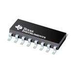
| 描述 | IC SONAR RANGING CONTROL 16-SOIC |
| 产品分类 | |
| 品牌 | Texas Instruments |
| 数据手册 | |
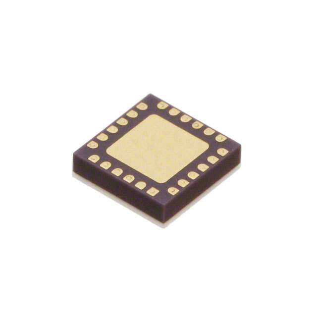
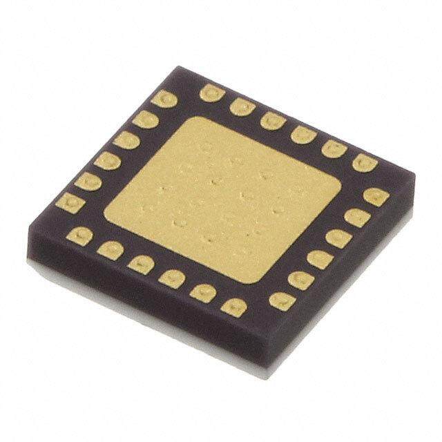
| 产品图片 |
|
| 产品型号 | TL851CDR |
| RF类型 | 声纳控制 |
| rohs | 无铅 / 符合限制有害物质指令(RoHS)规范要求 |
| 产品系列 | - |
| 产品培训模块 | http://www.digikey.cn/PTM/IndividualPTM.page?site=cn&lang=zhs&ptm=26085 |
| 产品目录页面 | |
| 供应商器件封装 | 16-SOIC N |
| 其它名称 | 296-18895-6 |
| 制造商产品页 | http://www.ti.com/general/docs/suppproductinfo.tsp?distId=10&orderablePartNumber=TL851CDR |
| 功能 | 声纳测距接收器 |
| 包装 | Digi-Reel® |
| 封装/外壳 | 16-SOIC(0.154",3.90mm 宽) |
| 标准包装 | 1 |
| 辅助属性 | TTL 兼容 |
| 频率 | 20kHz ~ 90kHz |


- 商务部:美国ITC正式对集成电路等产品启动337调查
- 曝三星4nm工艺存在良率问题 高通将骁龙8 Gen1或转产台积电
- 太阳诱电将投资9.5亿元在常州建新厂生产MLCC 预计2023年完工
- 英特尔发布欧洲新工厂建设计划 深化IDM 2.0 战略
- 台积电先进制程称霸业界 有大客户加持明年业绩稳了
- 达到5530亿美元!SIA预计今年全球半导体销售额将创下新高
- 英特尔拟将自动驾驶子公司Mobileye上市 估值或超500亿美元
- 三星加码芯片和SET,合并消费电子和移动部门,撤换高东真等 CEO
- 三星电子宣布重大人事变动 还合并消费电子和移动部门
- 海关总署:前11个月进口集成电路产品价值2.52万亿元 增长14.8%


PDF Datasheet 数据手册内容提取
TL851 SONAR RANGING CONTROL SLSS004 – SEPTEMBER 1983 – REVISED MARCH 1988 (cid:1) Designed for Use With the TL852 in Sonar N PACKAGE Ranging Modules Like the SN28827 (TOP VIEW) (cid:1) Operates With Single Supply (cid:1) VCC 1 16 BLNK Accurate Clock Output for External Use XMIT 2 15 BINH (cid:1) Synchronous 4-Bit Gain Control Output GND 3 14 INIT (cid:1) Internal 1.2-V Level Detector for Receive GCD 4 13 FILT (cid:1) TTL-Compatible GCA 5 12 XTAL2 (cid:1) GCB 6 11 XTAL1 Interfaces to Electrostatic or Piezoelectric GCC 7 10 OSC Transducers REC 8 9 ECHO description The TL851 is an economical digital I2L ranging control integrated circuit designed for use with the Texas Instruments TL852 sonar ranging receiver integrated circuit. The TL851 is designed for distance measurement from six inches to 35 feet. The device has an internal oscillator that uses a low-cost external ceramic resonator. With a simple interface and a 420-kHz ceramic resonator, the device will drive a 50-kHz electrostatic transducer. The device cycle begins when Initiate (INIT) is taken to the high logic level. There must be at least 5 ms from initial power-up (V ) to the first initiate signal in order for all the device internal latches to reset and for the CC ceramic-resonator-controlled oscillator to stabilize. The device will transmit a burst of 16 pulses each time INIT is taken high. The oscillator output (OSC) is enabled by INIT. The oscillator frequency is the ceramic resonator frequency divided by 8.5 for the first 16 cycles (during transmit) and then the oscillator frequency changes to the ceramic resonator frequency divided by 4.5 for the remainder of the device cycle. When used with an external 420-kHz ceramic resonator, the device internal blanking disables the receive input (REC) for 3.8 ms after initiate to exclude false receive inputs that may be caused by transducer ringing. The internal blanking feature also eliminates echos from objects closer than 1.3 feet from the transducer. If it is necessary to detect objects closer than 1.3 feet, then the internal blanking may be shortened by taking the blanking inhibit (BINH) high, enabling the receive input. The blanking input (BLNK) may be used to disable the receive input and reset ECHO to a low logic level at any time during the device cycle for selective echo exclusion or for a multiple-echo mode of operation. The device provides a synchronous 4-bit gain control output (12 steps) designed to control the gain of the TL852 sonar ranging receiver integrated circuit. The digital gain control waveforms are shown in Figure 2 with the nominal transition times from INIT listed in the Gain Control Output Table. The threshold of the internal receive level detector is 1.2 V. The TL851 operates over a supply voltage range of 4.5 V to 6.8 V and is characterized for operation from 0°C to 40°C. PRODUCTION DATA information is current as of publication date. Copyright 1988, Texas Instruments Incorporated Products conform to specifications per the terms of Texas Instruments standard warranty. Production processing does not necessarily include testing of all parameters. POST OFFICE BOX 655303 • DALLAS, TEXAS 75265 1
TL851 SONAR RANGING CONTROL SLSS004 – SEPTEMBER 1983 – REVISED MARCH 1988 GAIN CONTROL OUTPUT TABLE STEP TIME (ms) GCD GCC GCB GCA NUMBER FROM INITIATE↑† 0 L L L L 2.38 ms 1 L L L H 5.12 ms 2 L L L L 7.87 ms 3 L L H H 10.61 ms 4 L H L L 13.35 ms 5 L H L H 16.09 ms 6 L H H L 18.84 ms 7 L H H H 21.58 ms 8 H L L L 27.07 ms 9 H L L H 32.55 ms 10 H L H L 38.04 ms 11 H L H H INIT ↓ †This is the time to the end of the indicated step and assumes a nominal 420-kHz ceramic resonator. functional block diagram FILT VCC 13 1 Filtered Supply 10 OSC 420-kHz Frequency Gain Step 2 Oscillator Divider Counter XMIT G 11 CT≤16 Transmit Enable XTAL1 5 GCA 6 + 8.5 GCB 12 7 XTAL2 + 4.5 + GCC 4 CLR GCD CT ≥ 208 14 INIT CLR CT > 16 Internal Blanking Blanking Latch 15 S BINH Echo 16 R BLNK Latch R 8 9 REC ECHO S 1.2 V 3 GND 2 POST OFFICE BOX 655303 • DALLAS, TEXAS 75265
TL851 SONAR RANGING CONTROL SLSS004 – SEPTEMBER 1983 – REVISED MARCH 1988 absolute maximum ratings over operating free-air temperature range (unless otherwise noted)† Voltage range at any pin with respect to GND . . . . . . . . . . . . . . . . . . . . . . . . . . . . . . . . . . . . . . . . . . – 0.5 V to 7 V Voltage range at any pin with respect to V . . . . . . . . . . . . . . . . . . . . . . . . . . . . . . . . . . . . . . . . . . – 7 V to 0.5 V CC Continuous total dissipation at (or below) 25°C free-air temperature (see Note 1) . . . . . . . . . . . . . . . 1150 mW Operating free-air temperature range . . . . . . . . . . . . . . . . . . . . . . . . . . . . . . . . . . . . . . . . . . . . . . . . . . 0°C to 40°C Storage temperature range . . . . . . . . . . . . . . . . . . . . . . . . . . . . . . . . . . . . . . . . . . . . . . . . . . . . . . . – 65°C to 150°C Lead temperature 1,6 mm (1/16 inch) from case for 10 seconds . . . . . . . . . . . . . . . . . . . . . . . . . . . . . . . 260°C †Stresses beyond those listed under absolute maximum ratings may cause permanent damage to the device. This is a stress rating only, and functional operation of the device at these or any other conditions beyond those indicated in the recommended operating conditions section of this specification is not implied. Exposure to absolute-maximum-rated conditions for extended periods may affect device reliability. NOTE 1: For operation above 25°C, derate linearly at the rate of 9.2 mW/°C. recommended operating conditions MIN MAX UNIT Supply voltage, VCC 4.5 6.8 V High-level input voltage, VIH BLNK, BINH, INIT 2.1 V Low-level input voltage, VIL BLNK, BINH, INIT 0.6 V Delay time, power up to INIT high 5 ms Operating free-air temperature, TA 0 40 °C electrical characteristics over recommended ranges of supply voltage and operating free-air temperature PARAMETER TEST CONDITIONS MIN TYP‡ MAX UNIT Input current BLNK, BINH, INIT VI = 2.1 V 1 mA High-level output current, IOH ECHO, OSC, GCA, GCB, GCC, GCD VOH = 5.5 V 100 m A Low-level output current, IOH ECHO, OSC, GCA, GCB, GCC, GCD IOL = 1.6 mA 0.4 V On-state output current SMIT output VO = 1 V –140 mA Internal blanking interval REC input 2.38§ ms OSC output 49.4§ FFrreeqquueennccyy dduurriinngg 1166-ppuullssee ttrraannssmmiitt ppeerriioodd kkHHzz XMIT output 49.4§ OSC output 93.3§ FFrreeqquueennccyy aafftteerr 1166-ppuullssee ttrraannssmmiitt ppeerriioodd kkHHzz XMIT output 0 During transmit period 260 SSuuppppllyy ccuurrrreenntt, IICCCC mmAA After transmit period 55 ‡Typical values are at VCC = 5 V and TA = 25°C. §These typical values apply for a 420-kHz ceramic resonator. POST OFFICE BOX 655303 • DALLAS, TEXAS 75265 3
TL851 SONAR RANGING CONTROL SLSS004 – SEPTEMBER 1983 – REVISED MARCH 1988 schematics of inputs and outputs EQUIVALENT OF BLNK, BINH AND TYPICAL OF ECHO, OSC, GCA, GCB, XMIT OUTPUTS INIT INPUTS GCC, AND GCD OUTPUTS VCC Ref Input Output 5 W Output 500 W Step No. 0 1 2 3 4 5 6 7 8 9 10 11 INIT GCA GCB GCC GCD Figure 1. Digital Gain Control Waveforms 4 POST OFFICE BOX 655303 • DALLAS, TEXAS 75265
TL851 SONAR RANGING CONTROL SLSS004 – SEPTEMBER 1983 – REVISED MARCH 1988 VCC INIT 16 Pulses XMIT (L) BINH (L) BLNK Internal Blanking ≈2.38 ms ≈1.2 V REC (Input from TL852) ECHO Figure 2. Example of Single-Echo-Mode Cycle When Used With the TL852 Receiver and 420-kHz Ceramic Resonator POST OFFICE BOX 655303 • DALLAS, TEXAS 75265 5
PACKAGE OPTION ADDENDUM www.ti.com 6-Feb-2020 PACKAGING INFORMATION Orderable Device Status Package Type Package Pins Package Eco Plan Lead/Ball Finish MSL Peak Temp Op Temp (°C) Device Marking Samples (1) Drawing Qty (2) (6) (3) (4/5) TL851CD ACTIVE SOIC D 16 40 Green (RoHS NIPDAU Level-1-260C-UNLIM TL851C & no Sb/Br) TL851CDR ACTIVE SOIC D 16 2500 Green (RoHS NIPDAU Level-1-260C-UNLIM TL851C & no Sb/Br) TL851CDR ACTIVE SOIC D 16 2500 Green (RoHS NIPDAU Level-1-260C-UNLIM TL851C & no Sb/Br) TL851CDRG4 ACTIVE SOIC D 16 2500 Green (RoHS NIPDAU Level-1-260C-UNLIM TL851C & no Sb/Br) TL851CDRG4 ACTIVE SOIC D 16 2500 Green (RoHS NIPDAU Level-1-260C-UNLIM TL851C & no Sb/Br) TL851CN ACTIVE PDIP N 16 25 Green (RoHS NIPDAU N / A for Pkg Type TL851CN & no Sb/Br) TL851CN ACTIVE PDIP N 16 25 Green (RoHS NIPDAU N / A for Pkg Type TL851CN & no Sb/Br) TL851CNE4 ACTIVE PDIP N 16 25 Green (RoHS NIPDAU N / A for Pkg Type TL851CN & no Sb/Br) TL851CNE4 ACTIVE PDIP N 16 25 Green (RoHS NIPDAU N / A for Pkg Type TL851CN & no Sb/Br) (1) The marketing status values are defined as follows: ACTIVE: Product device recommended for new designs. LIFEBUY: TI has announced that the device will be discontinued, and a lifetime-buy period is in effect. NRND: Not recommended for new designs. Device is in production to support existing customers, but TI does not recommend using this part in a new design. PREVIEW: Device has been announced but is not in production. Samples may or may not be available. OBSOLETE: TI has discontinued the production of the device. (2) RoHS: TI defines "RoHS" to mean semiconductor products that are compliant with the current EU RoHS requirements for all 10 RoHS substances, including the requirement that RoHS substance do not exceed 0.1% by weight in homogeneous materials. Where designed to be soldered at high temperatures, "RoHS" products are suitable for use in specified lead-free processes. TI may reference these types of products as "Pb-Free". RoHS Exempt: TI defines "RoHS Exempt" to mean products that contain lead but are compliant with EU RoHS pursuant to a specific EU RoHS exemption. Green: TI defines "Green" to mean the content of Chlorine (Cl) and Bromine (Br) based flame retardants meet JS709B low halogen requirements of <=1000ppm threshold. Antimony trioxide based flame retardants must also meet the <=1000ppm threshold requirement. (3) MSL, Peak Temp. - The Moisture Sensitivity Level rating according to the JEDEC industry standard classifications, and peak solder temperature. Addendum-Page 1
PACKAGE OPTION ADDENDUM www.ti.com 6-Feb-2020 (4) There may be additional marking, which relates to the logo, the lot trace code information, or the environmental category on the device. (5) Multiple Device Markings will be inside parentheses. Only one Device Marking contained in parentheses and separated by a "~" will appear on a device. If a line is indented then it is a continuation of the previous line and the two combined represent the entire Device Marking for that device. (6) Lead/Ball Finish - Orderable Devices may have multiple material finish options. Finish options are separated by a vertical ruled line. Lead/Ball Finish values may wrap to two lines if the finish value exceeds the maximum column width. Important Information and Disclaimer:The information provided on this page represents TI's knowledge and belief as of the date that it is provided. TI bases its knowledge and belief on information provided by third parties, and makes no representation or warranty as to the accuracy of such information. Efforts are underway to better integrate information from third parties. TI has taken and continues to take reasonable steps to provide representative and accurate information but may not have conducted destructive testing or chemical analysis on incoming materials and chemicals. TI and TI suppliers consider certain information to be proprietary, and thus CAS numbers and other limited information may not be available for release. In no event shall TI's liability arising out of such information exceed the total purchase price of the TI part(s) at issue in this document sold by TI to Customer on an annual basis. Addendum-Page 2
PACKAGE MATERIALS INFORMATION www.ti.com 26-Feb-2019 TAPE AND REEL INFORMATION *Alldimensionsarenominal Device Package Package Pins SPQ Reel Reel A0 B0 K0 P1 W Pin1 Type Drawing Diameter Width (mm) (mm) (mm) (mm) (mm) Quadrant (mm) W1(mm) TL851CDR SOIC D 16 2500 330.0 16.4 6.5 10.3 2.1 8.0 16.0 Q1 PackMaterials-Page1
PACKAGE MATERIALS INFORMATION www.ti.com 26-Feb-2019 *Alldimensionsarenominal Device PackageType PackageDrawing Pins SPQ Length(mm) Width(mm) Height(mm) TL851CDR SOIC D 16 2500 350.0 350.0 43.0 PackMaterials-Page2
None
None
None
IMPORTANTNOTICEANDDISCLAIMER TI PROVIDES TECHNICAL AND RELIABILITY DATA (INCLUDING DATASHEETS), DESIGN RESOURCES (INCLUDING REFERENCE DESIGNS), APPLICATION OR OTHER DESIGN ADVICE, WEB TOOLS, SAFETY INFORMATION, AND OTHER RESOURCES “AS IS” AND WITH ALL FAULTS, AND DISCLAIMS ALL WARRANTIES, EXPRESS AND IMPLIED, INCLUDING WITHOUT LIMITATION ANY IMPLIED WARRANTIES OF MERCHANTABILITY, FITNESS FOR A PARTICULAR PURPOSE OR NON-INFRINGEMENT OF THIRD PARTY INTELLECTUAL PROPERTY RIGHTS. These resources are intended for skilled developers designing with TI products. You are solely responsible for (1) selecting the appropriate TI products for your application, (2) designing, validating and testing your application, and (3) ensuring your application meets applicable standards, and any other safety, security, or other requirements. These resources are subject to change without notice. TI grants you permission to use these resources only for development of an application that uses the TI products described in the resource. Other reproduction and display of these resources is prohibited. No license is granted to any other TI intellectual property right or to any third party intellectual property right. TI disclaims responsibility for, and you will fully indemnify TI and its representatives against, any claims, damages, costs, losses, and liabilities arising out of your use of these resources. TI’s products are provided subject to TI’s Terms of Sale (www.ti.com/legal/termsofsale.html) or other applicable terms available either on ti.com or provided in conjunction with such TI products. TI’s provision of these resources does not expand or otherwise alter TI’s applicable warranties or warranty disclaimers for TI products. Mailing Address: Texas Instruments, Post Office Box 655303, Dallas, Texas 75265 Copyright © 2020, Texas Instruments Incorporated