ICGOO在线商城 > 射频/IF 和 RFID > RF 其它 IC 和模块 > AD6643BCPZ-250
 Datasheet下载
- 型号: AD6643BCPZ-250
- 制造商: Analog
- 库位|库存: xxxx|xxxx
- 要求:
| 数量阶梯 | 香港交货 | 国内含税 |
| +xxxx | $xxxx | ¥xxxx |
查看当月历史价格
查看今年历史价格
AD6643BCPZ-250产品简介:
ICGOO电子元器件商城为您提供AD6643BCPZ-250由Analog设计生产,在icgoo商城现货销售,并且可以通过原厂、代理商等渠道进行代购。 AD6643BCPZ-250价格参考¥610.54-¥706.65。AnalogAD6643BCPZ-250封装/规格:RF 其它 IC 和模块, RF IC IF Receiver CDMA, CDMA2000, LTE, WiMAX Sample Rates to 250MSPS 64-LFCSP-VQ (9x9)。您可以下载AD6643BCPZ-250参考资料、Datasheet数据手册功能说明书,资料中有AD6643BCPZ-250 详细功能的应用电路图电压和使用方法及教程。
AD6643BCPZ-250 是由 Analog Devices Inc.(现为 ADI,亚德诺半导体)生产的一款高性能射频 (RF) 和中频 (IF) 模拟信号处理芯片,属于 RF 其他 IC 和模块类别。其主要应用场景包括:

1. 通信系统:
   - 适用于无线通信基站、软件定义无线电(SDR)、卫星通信等场景。
   - 支持高速数据采集和信号处理,满足现代通信系统对高带宽和低延迟的需求。

2. 雷达与电子战系统:
   - 用于脉冲雷达、连续波雷达以及电子对抗设备中,提供快速信号采样和精确的信号分析能力。
   - 能够处理复杂的调制信号,提升目标检测精度和抗干扰能力。

3. 测试与测量设备:
   - 在频谱分析仪、矢量信号分析仪和其他高端测试仪器中应用广泛。
   - 提供高采样率和动态范围,确保测试结果的准确性和可靠性。

4. 医疗成像:
   - 应用于超声成像、核磁共振(MRI)等医疗设备中,支持实时信号采集和处理。
   - 高分辨率特性有助于生成更清晰的图像,提高诊断准确性。

5. 航空航天与国防:
   - 用于导航系统、飞行器通信链路以及遥感技术中。
   - 具备优异的环境适应性,能够在极端条件下稳定运行。

AD6643BCPZ-250 的核心优势在于其高达 250 MSPS 的采样速率、12 位分辨率以及出色的信噪比(SNR)性能,使其成为需要高精度和高速度信号处理的应用的理想选择。
| 参数 | 数值 |
| 产品目录 | |
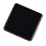
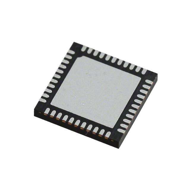
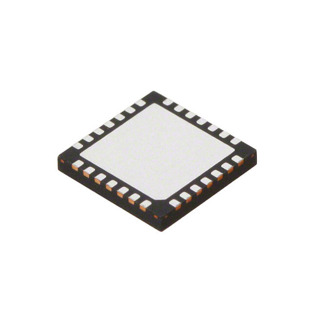
| 描述 | IC IF RCVR 11BIT 250MSPS 64LFCSP模数转换器 - ADC IC 11 Bit IF Diversity 3G Rcvr |
| 产品分类 | |
| 品牌 | Analog Devices |
| 产品手册 | |
| 产品图片 |
|
| rohs | 符合RoHS无铅 / 符合限制有害物质指令(RoHS)规范要求 |
| 产品系列 | 数据转换器IC,模数转换器 - ADC,Analog Devices AD6643BCPZ-250- |
| 数据手册 | |
| 产品型号 | AD6643BCPZ-250 |
| RF类型 | CDMA,CDMA2000,LTE,WiMAX |
| 产品种类 | 模数转换器 - ADC |
| 供应商器件封装 | 64-LFCSP-VQ(9x9) |
| 信噪比 | 74.8 dB |
| 其它名称 | AD6643BCPZ250 |
| 分辨率 | 11 bit |
| 功能 | IF 接收器 |
| 包装 | 托盘 |
| 商标 | Analog Devices |
| 安装风格 | SMD/SMT |
| 封装 | Tray |
| 封装/外壳 | 64-VFQFN 裸露焊盘,CSP |
| 封装/箱体 | LFCSP-64 |
| 工作电源电压 | 1.7 V to 1.9 V |
| 工厂包装数量 | 260 |
| 接口类型 | SPI |
| 最大功率耗散 | 853 mW |
| 最大工作温度 | + 85 C |
| 最小工作温度 | - 40 C |
| 标准包装 | 1 |
| 系列 | AD6643 |
| 结构 | Pipeline |
| 视频文件 | http://www.digikey.cn/classic/video.aspx?PlayerID=1364138032001&width=640&height=505&videoID=2245193150001 |
| 转换速率 | 250 MS/s |
| 辅助属性 | 采样率达 250MSPS |
| 输入类型 | Single-Ended/Differential |
| 通道数量 | 2 Channel |
| 频率 | - |


- 商务部:美国ITC正式对集成电路等产品启动337调查
- 曝三星4nm工艺存在良率问题 高通将骁龙8 Gen1或转产台积电
- 太阳诱电将投资9.5亿元在常州建新厂生产MLCC 预计2023年完工
- 英特尔发布欧洲新工厂建设计划 深化IDM 2.0 战略
- 台积电先进制程称霸业界 有大客户加持明年业绩稳了
- 达到5530亿美元!SIA预计今年全球半导体销售额将创下新高
- 英特尔拟将自动驾驶子公司Mobileye上市 估值或超500亿美元
- 三星加码芯片和SET,合并消费电子和移动部门,撤换高东真等 CEO
- 三星电子宣布重大人事变动 还合并消费电子和移动部门
- 海关总署:前11个月进口集成电路产品价值2.52万亿元 增长14.8%


PDF Datasheet 数据手册内容提取
Dual IF Receiver Data Sheet AD6643 FEATURES FUNCTIONAL BLOCK DIAGRAM 11-bit, 250 MSPS output data rate per channel AVDD AGND DRVDD Performance with NSR enabled AD6643 SNR: 74.5 dBFS in a 55 MHz band to 90 MHz at 250 MSPS DCO± RS PeSrfNoRrm: 7a2n.0ce d wBFitSh iNn SaR 8 d2i sMaHbzle bda nd to 90 MHz at 250 MSPS VVIINN+–AA PIPAEDLCINE 14 NROEIQSEU ASNHTAIPZIENRG 11 PLEXERIVER D0± SNR: 66.2 dBFS up to 90 MHz at 250 MSPS VCM ULTIDS D ToStaFlD pRo:w 8e5r d cBocn usupm top t1i8o5n :M 7H06z amtW 25 a0t M20S0P SM SPS VVIINN+–BB PIPAEDLCINE 14 NROEIQSEU ASNHTAIPZIENRG 11 DATA MAND LV D10± 1.8 V supply voltages OEB LVDS (ANSI-644 levels) outputs REFERENCE CLOCK SYNC Integer 1-to-8 input clock divider (625 MHz maximum input) DIVIDER Internal ADC voltage reference SERIAL PORT PDWN Flexible analog input range 1.4 V p-p to 2.0 V p-p (1.75 V p-p nominal) SCLK SDIO CSB CLK+ CLK– D95if fdeBr ecnhtainaln aenl aisloolga tiniopnu/tcsr owsisttha 4lk0 0 MHz bandwidth N1 . O TATHNEEDS DC0H±A TNON EDL1 0B± LPVINDSS ROEUPTRPEUSTE DNATT BAO.TH THE CHANNEL A 09638-001 Figure 1. Serial port control Energy saving power-down modes APPLICATIONS Communications Diversity radio and smart antenna (MIMO) systems Multimode digital receivers (3G) WCDMA, LTE, CDMA2000 WiMAX, TD-SCDMA I/Q demodulation systems General-purpose software radios GENERAL DESCRIPTION The AD6643 is an 11-bit, 200 MSPS/250 MSPS, dual-channel Each ADC output is connected internally to an NSR block. The intermediate frequency (IF) receiver specifically designed to integrated NSR circuitry allows for improved SNR performance in support multi-antenna systems in telecommunication a smaller frequency band within the Nyquist bandwidth. The applications where high dynamic range performance, low power, device supports two different output modes selectable via the SPI. and small size are desired. With the NSR feature enabled, the outputs of the ADCs are processed such that the AD6643 supports enhanced SNR per- The device consists of two high performance analog-to-digital formance within a limited portion of the Nyquist bandwidth converters (ADCs) and noise shaping requantizer (NSR) digital while maintaining an 11-bit output resolution. blocks. Each ADC consists of a multistage, differential pipelined architecture with integrated output error correction logic, and The NSR block can be programmed to provide a bandwidth each ADC features a wide bandwidth switched capacitor sampling of either 22% or 33% of the sample clock. For example, with a network within the first stage of the differential pipeline. An sample clock rate of 185 MSPS, the AD6643 can achieve up to integrated voltage reference eases design considerations. A duty 75.5 dBFS SNR for a 40 MHz bandwidth in the 22% mode and cycle stabilizer (DCS) compensates for variations in the ADC up to 73.7 dBFS SNR for a 60 MHz bandwidth in the 33% mode. clock duty cycle, allowing the converters to maintain excellent (continued on Page 3) performance. Rev. C Document Feedback Information furnished by Analog Devices is believed to be accurate and reliable. However, no responsibility is assumed by Analog Devices for its use, nor for any infringements of patents or other One Technology Way, P.O. Box 9106, Norwood, MA 02062-9106, U.S.A. rights of third parties that may result from its use. Specifications subject to change without notice. No license is granted by implication or otherwise under any patent or patent rights of Analog Devices. Tel: 781.329.4700 ©2011–2012 Analog Devices, Inc. All rights reserved. Trademarks and registered trademarks are the property of their respective owners. Technical Support www.analog.com
AD6643 Data Sheet TABLE OF CONTENTS Features .............................................................................................. 1 Voltage Reference ....................................................................... 23 Applications ....................................................................................... 1 Clock Input Considerations ...................................................... 23 General Description ......................................................................... 1 Power Dissipation and Standby Mode .................................... 24 Functional Block Diagram .............................................................. 1 Digital Outputs ........................................................................... 25 Revision History ............................................................................... 2 ADC Overrange (OR) ................................................................ 25 Product Highlights ........................................................................... 3 Noise Shaping Requantizer (NSR) ............................................... 26 Specifications ..................................................................................... 4 22% BW Mode (>40 MHz at 184.32 MSPS) ........................... 26 ADC DC Specifications ................................................................. 4 33% BW Mode (>60 MHz at 184.32 MSPS) ........................... 27 ADC AC Specifications ................................................................. 5 Channel/Chip Synchronization .................................................... 28 Digital Specifications—AD6643-200/AD6643-250 ..................... 6 Serial Port Interface (SPI) .............................................................. 29 Switching Specifications ................................................................ 8 Configuration Using the SPI ..................................................... 29 Timing Specifications—AD6643-200/AD6643-250 ................ 8 Hardware Interface ..................................................................... 29 Absolute Maximum Ratings .......................................................... 10 SPI Accessible Features .............................................................. 30 Thermal Characteristics ............................................................ 10 Memory Map .................................................................................. 31 ESD Caution ................................................................................ 10 Reading the Memory Map Register Table ............................... 31 Pin Configurations and Function Descriptions ......................... 11 Memory Map Register Table ..................................................... 32 Typical Performance Characteristics ........................................... 15 Memory Map Register Description ......................................... 35 Equivalent Circuits ......................................................................... 20 Applications Information .............................................................. 36 Theory of Operation ...................................................................... 21 Design Guidelines ...................................................................... 36 ADC Architecture ...................................................................... 21 Outline Dimensions ....................................................................... 37 Analog Input Considerations .................................................... 21 Ordering Guide .......................................................................... 37 REVISION HISTORY 11/12—Rev. B to Rev. C Changes to Figure 2 ........................................................................... 9 Change to OEB Pin Description, Table 8 .................................... 12 Changes to Features Section............................................................. 1 Changes Figure 5 and Table 9 ....................................................... 13 Change to Table 1 ................................................................................ Changes to Typical Performance Characteristics Conditions Changes to Table 4 ............................................................................. 8 Summary ......................................................................................... 15 Changes to Reading the Memory Map Register Table Added AD6643-200 Throughout ................................................. 15 Section ............................................................................................... 31 Changes to Figure 24 and Figure 25 ............................................ 18 Deleted Registers 0x0E, 0x24, and 0x25, Table 14 ....................... 33 Changes to Theory of Operation Section.................................... 19 Change to Memory Map Register Description Section.............. 36 Changes to Timing Section ........................................................... 23 Updated Outline Dimensions ........................................................ 37 Added ADC Overrange (OR) Section ......................................... 23 6/12—Rev. A to Rev. B Changed Frequency (Hz) to Frequency (MHz) in Figure 39, Changes to Features .......................................................................... 1 Figure 40, and Figure 41 ................................................................ 24 Changes to Full Power Bandwidth Parameter, Deleted Noise Changed Frequency (Hz) to Frequency (MHz) in Figure 42, Bandwidth Parameter, Changes to Endnote 3; Table 2 ............... 6 Figure 43, and Figure 44 ................................................................ 25 Added Figure 20 to Figure 33; Renumbered Sequentially ........ 17 Changes to Channel/Chip Synchronization Section ................. 26 Changes to Figure 52 ...................................................................... 24 Changed 0x59 to 0x3E Throughout ............................................. 29 Updated Outline Dimensions ....................................................... 35 Changes to 0x02, Bits[5:4] and 0x16, Bit 5 in Table 14 ............. 30 Deleted 0x59, Table 14 ................................................................... 32 9/11—Rev. 0 to Rev. A Deleted SYNC Pin Control (Register 0x59) Section .................. 33 Added 250 MSPS Speed Grade Throughout................................. 1 Changes to Ordering Guide .......................................................... 35 Changes to Table 1 ............................................................................ 4 4/11—Revision 0: Initial Version Changes to Table 2 ............................................................................ 5 Changes to Table 4 ............................................................................ 8 Rev. C | Page 2 of 40
Data Sheet AD6643 When the NSR block is disabled, the ADC data is provided directly The AD6643 is available in a Pb-free, RoHS-compliant, 64-lead, to the output at a resolution of 11 bits. The AD6643 can achieve 9 mm × 9 mm lead frame chip scale package (LFCSP_VQ) and is up to 66.5 dBFS SNR for the entire Nyquist bandwidth when specified over the industrial temperature range of −40°C to +85°C. operated in this mode. This allows the AD6643 to be used in This product is protected by a U.S. patent. telecommunication applications such as a digital predistortion PRODUCT HIGHLIGHTS observation path where wider bandwidths are required. 1. Two ADCs are contained in a small, space-saving, After digital signal processing, multiplexed output data is 9 mm × 9 mm × 0.85 mm, 64-lead LFCSP package. routed into two 11-bit output ports such that the maximum 2. Pin selectable noise shaping requantizer (NSR) function data rate is 400 Mbps (DDR). These outputs are LVDS and that allows for improved SNR within a reduced bandwidth support ANSI-644 levels. of up to 60 MHz at 185 MSPS. The AD6643 receiver digitizes a wide spectrum of IF frequencies. 3. LVDS digital output interface configured for low cost Each receiver is designed for simultaneous reception of a separate FPGA families. antenna. This IF sampling architecture greatly reduces compo- 4. Operation from a single 1.8 V supply. nent cost and complexity compared with traditional analog 5. Standard serial port interface (SPI) that supports various techniques or less integrated digital methods. product features and functions, such as data formatting (offset binary or twos complement), NSR, power-down, Flexible power-down options allow significant power savings. test modes, and voltage reference mode. Programming for device setup and control is accomplished using a 3-wire SPI-compatible serial interface with numerous 6. On-chip integer 1-to-8 input clock divider and multichip sync function to support a wide range of clocking schemes modes to support board level system testing. and multichannel subsystems. Rev. C | Page 3 of 40
AD6643 Data Sheet SPECIFICATIONS ADC DC SPECIFICATIONS AVDD = 1.8 V, DRVDD = 1.8 V, maximum sample rate, VIN = −1.0 dBFS differential input, 1.75 V p-p full-scale input range, default SPI, unless otherwise noted. Table 1. AD6643-200 AD6643-250 Parameter Temperature Min Typ Max Min Typ Max Unit RESOLUTION Full 11 11 Bits ACCURACY No Missing Codes Full Guaranteed Guaranteed Offset Error Full ±10 ±10 mV Gain Error Full +2/−6 −5/+3 % FSR Differential Nonlinearity (DNL)1 Full ±0.1 ±0.25 ±0.1 ±0.4 LSB Integral Nonlinearity (INL)1 Full ±0.2 ±0.25 ±0.2 ±0.4 LSB MATCHING CHARACTERISTIC Offset Error 25°C ±13 ±13 mV Gain Error 25°C −2/+3.5 −2.5/+3.5 % FSR TEMPERATURE DRIFT Offset Error Full ±15 ±15 ppm/°C Gain Error Full ±87 ±87 ppm/°C INPUT REFERRED NOISE VREF = 1.75 V 25°C 0.614 0.614 LSB rms ANALOG INPUT Input Span Full 1.75 1.75 V p-p Input Capacitance2 Full 2.5 2.5 pF Input Resistance3 Full 20 20 kΩ Input Common-Mode Voltage Full 0.9 0.9 V POWER SUPPLIES Supply Voltage AVDD Full 1.7 1.8 1.9 1.7 1.8 1.9 V DRVDD Full 1.7 1.8 1.9 1.7 1.8 1.9 V Supply Current I 1 Full 238 260 256 275 mA AVDD I 1 (NSR Disabled) Full 154 215 180 215 mA DRVDD I 1 (NSR Enabled—22% Mode) Full 172 206 mA DRVDD I 1 (NSR Enabled—33% Mode) Full 186 218 mA DRVDD POWER CONSUMPTION Sine Wave Input1 (DRVDD = 1.8 V, Full 706 855 785 873 mW NSR Disabled) Sine Wave Input1 (DRVDD = 1.8 V, Full 738 832 mW NSR Enabled—22% Mode) Sine Wave Input1 (DRVDD = 1.8 V, Full 765 853 mW NSR Enabled—33% Mode) Standby Power4 Full 90 90 mW Power-Down Power Full 10 10 mW 1 Measured using a 10 MHz, 0 dBFS sine wave, and 100 Ω termination on each LVDS output pair. 2 Input capacitance refers to the effective capacitance between one differential input pin and its complement. 3 Input resistance refers to the effective resistance between one differential input pin and its complement. 4 Standby power is measured using a dc input and the CLK± pins inactive (set to AVDD or AGND). Rev. C | Page 4 of 40
Data Sheet AD6643 ADC AC SPECIFICATIONS AVDD = 1.8 V, DRVDD = 1.8 V, maximum sample rate, VIN = −1.0 dBFS differential input, 1.75 V p-p full-scale input range, default SPI, unless otherwise noted. Table 2. AD6643-200 AD6643-250 Parameter1 Temperature Min Typ Max Min Typ Max Unit SIGNAL-TO-NOISE-RATIO (SNR) NSR Disabled f = 30 MHz 25°C 66.6 66.4 dBFS IN f = 90 MHz 25°C 66.5 66.2 dBFS IN Full 66.2 dBFS f = 140 MHz 25°C 66.4 66.1 dBFS IN f = 185 MHz 25°C 66.2 65.9 dBFS IN Full 65.3 dBFS f = 220 MHz 25°C 66.0 65.6 dBFS IN NSR Enabled 22% BW Mode f = 30 MHz 25°C 76.1 74.8 dBFS IN f = 90 MHz 25°C 76.1 74.5 dBFS IN Full 74.5 dBFS f = 140 MHz 25°C 75.5 74.2 dBFS IN f = 185 MHz 25°C 74.7 73.7 dBFS IN Full 72.6 dBFS f = 220 MHz 25°C 74.2 73.4 dBFS IN 33% BW Mode f = 30 MHz 25°C 76.1 72.3 dBFS IN f = 90 MHz 25°C 73.6 72.0 dBFS IN Full 72.0 dBFS f = 140 MHz 25°C 73.1 71.7 dBFS IN f = 185 MHz 25°C 72.6 71.2 dBFS IN Full 70.1 dBFS f = 220 MHz 25°C 72.1 70.9 dBFS IN SIGNAL-TO-NOISE-AND-DISTORTION (SINAD) f = 30 MHz 25°C 65.6 65.4 dBFS IN f = 90 MHz 25°C 65.5 65.2 dBFS IN Full 65.1 dBFS f = 140 MHz 25°C 65.3 65.1 dBFS IN f = 185 MHz 25°C 65.1 64.9 dBFS IN Full 64.3 dBFS f = 220 MHz 25°C 64.9 64.6 dBFS IN WORST SECOND OR THIRD HARMONIC f = 30 MHz 25°C −92 −90 dBc IN f = 90 MHz 25°C −91 −88 dBc IN Full −80 dBc f = 140 MHz 25°C −88 −86 dBc IN f = 185 MHz 25°C −88 −85 dBc IN Full −80 dBc f = 220 MHz 25°C −84 −85 dBc IN Rev. C | Page 5 of 40
AD6643 Data Sheet AD6643-200 AD6643-250 Parameter1 Temperature Min Typ Max Min Typ Max Unit SPURIOUS-FREE DYNAMIC RANGE (SFDR) f = 30 MHz 25°C 92 90 dBc IN f = 90 MHz 25°C 91 88 dBc IN Full 80 dBc f = 140 MHz 25°C 88 86 dBc IN f = 185 MHz 25°C 88 85 dBc IN Full 79 dBc f = 220 MHz 25°C 84 85 dBc IN WORST OTHER HARMONIC OR SPUR f = 30 MHz 25°C −94 −94 dBc IN f = 90 MHz 25°C −94 −93 dBc IN Full −80 dBc f = 140 MHz 25°C −95 −92 dBc IN f = 185 MHz 25°C −94 −92 dBc IN Full −80 dBc f = 220 MHz 25°C −93 −88 dBc IN TWO TONE SFDR f = 184.12 MHz, 187.12 MHz (−7 dBFS) 25°C 88 88 dBc IN CROSSTALK2 Full 95 95 dB FULL POWER BANDWIDTH3 25°C 1000 1000 MHz 1 For a complete set of definitions, see the AN-835 Application Note, Understanding High Speed ADC Testing and Evaluation. 2 Crosstalk is measured at 100 MHz with −1 dBFS on one channel and with no input on the alternate channel. 3 Full power bandwidth is the bandwidth for the ADC inputs at which the spectral power of the fundamental frequency is reduced by 3 dB. DIGITAL SPECIFICATIONS—AD6643-200/AD6643-250 AVDD = 1.8 V, DRVDD = 1.8 V, maximum sample rate, VIN = −1.0 dBFS differential input, 1.75 V p-p full-scale input range, DCS enabled, default SPI, unless otherwise noted. Table 3. Parameter Temperature Min Typ Max Unit DIFFERENTIAL CLOCK INPUTS (CLK+, CLK−) Logic Compliance CMOS/LVDS/LVPECL Internal Common-Mode Bias Full 0.9 V Differential Input Voltage Full 0.3 3.6 V p-p Input Voltage Range Full AGND AVDD V Input Common-Mode Range Full 0.9 1.4 V Input Current Level High Full 10 22 µA Low Full −22 −10 µA Input Capacitance Full 4 pF Input Resistance Full 8 10 12 kΩ SYNC INPUT Logic Compliance CMOS/LVDS Internal Bias Full 0.9 V Input Voltage Range Full AGND AVDD V Input Voltage Level High Full 1.2 AVDD V Low Full AGND 0.6 V Rev. C | Page 6 of 40
Data Sheet AD6643 Parameter Temperature Min Typ Max Unit Input Current Level High Full −5 +5 µA Low Full −100 +100 µA Input Capacitance Full 1 pF Input Resistance Full 12 16 20 kΩ LOGIC INPUT (CSB)1 Input Voltage Level High Full 1.22 2.1 V Low Full 0 0.6 V Input Current Level High Full −5 +5 µA Low Full −80 −45 µA Input Resistance Full 26 kΩ Input Capacitance Full 2 pF LOGIC INPUT (SCLK)2 Input Voltage Level High Full 1.22 2.1 V Low Full 0 0.6 V Input Current Level High Full 45 70 µA Low Full −5 +5 µA Input Resistance Full 26 kΩ Input Capacitance Full 2 pF LOGIC INPUTS (SDIO)1 Input Voltage Level High Full 1.22 2.1 V Low Full 0 0.6 V Input Current Level High Full 45 70 µA Low Full −5 +5 µA Input Resistance Full 26 kΩ Input Capacitance Full 5 pF LOGIC INPUTS (OEB, PDWN)2 Input Voltage Level High Full 1.22 2.1 V Low Full 0 0.6 V Input Current Level High Full 45 70 µA Low Full −5 +5 µA Input Resistance Full 26 kΩ Input Capacitance Full 5 pF DIGITAL OUTPUTS LVDS Data and OR Outputs Differential Output Voltage (VOD) ANSI Mode Full 250 350 450 mV Reduced Swing Mode Full 150 200 280 mV Output Offset Voltage (VOS) ANSI Mode Full 1.15 1.25 1.35 V Reduced Swing Mode Full 1.15 1.25 1.35 V 1 Pull up. 2 Pull down. Rev. C | Page 7 of 40
AD6643 Data Sheet SWITCHING SPECIFICATIONS Table 4. AD6643-200 AD6643-250 Parameter Symbol Temperature Min Typ Max Min Typ Max Unit CLOCK INPUT PARAMETERS Input Clock Rate Full 625 625 MHz Conversion Rate1 Full 40 200 40 250 MSPS CLK Period—Divide-by-1 Mode2 t Full 4.0 4 ns CLK CLK Pulse Width High2 t CH Divide-by-1 Mode, DCS Enabled Full 2.25 2.5 2.75 1.8 2.0 2.2 ns Divide-by-1 Mode, DCS Disabled Full 2.375 2.5 2.625 1.9 2.0 2.1 ns Divide-by-2 Through Divide-by-8 Modes, DCS Full 0.8 0.8 ns Enabled DATA OUTPUT PARAMETERS (DATA, OR) 1.0 LVDS Mode 0.1 Data Propagation Delay2 t Full 6.0 6.0 ns PD DCO Propagation Delay2 t Full 6.7 6.7 ns DCO DCO to Data Skew2 tSKEW Full 0.4 0.7 1.0 0.4 0.7 1.0 ns Pipeline Delay (Latency) Full 10 10 Cycles3 NSR Enabled Full 13 13 Cycles3 Aperture Delay4 t Full 1.0 1.0 ns A Aperture Uncertainty (Jitter)4 t Full 0.1 0.1 ps rms J Wake-Up Time (from Standby) Full 10 10 μs Wake-Up Time (from Power-Down) Full 250 250 μs OUT-OF-RANGE RECOVERY TIME Full 3 3 Cycles 1 Conversion rate is the clock rate after the divider. 2 See Figure 2 for timing diagram. 3 Cycles refers to ADC input sample rate cycles. 4 Not shown in timing diagrams. TIMING SPECIFICATIONS—AD6643-200/AD6643-250 Table 5. Parameter Conditions Min Typ Max Unit SYNC TIMING REQUIREMENTS See Figure 3 for timing details t SYNC to the rising edge of CLK setup time 0.3 ns SSYNC t SYNC to the rising edge of CLK hold time 0.4 ns HSYNC SPI TIMING REQUIREMENTS See Figure 59 for SPI timing diagram t Setup time between the data and the rising edge of SCLK 2 ns DS t Hold time between the data and the rising edge of SCLK 2 ns DH t Period of the SCLK 40 ns CLK t Setup time between CSB and SCLK 2 ns S t Hold time between CSB and SCLK 2 ns H t Minimum period that SCLK should be in a logic high state 10 ns HIGH t Minimum period that SCLK should be in a logic low state 10 ns LOW t Time required for the SDIO pin to switch from an input to an output 10 ns EN_SDIO relative to the SCLK falling edge (not shown in Figure 59) t Time required for the SDIO pin to switch from an output to an input 10 ns DIS_SDIO relative to the SCLK rising edge (not shown in Figure 59) Rev. C | Page 8 of 40
Data Sheet AD6643 Timing Diagrams tA N – 1 N + 4 N + 5 N N + 3 VIN N + 1 N + 2 tCH tCLK CLK+ CLK– tDCO DCO– DCO+ tSKEW tPD PARALLEL INTERLEAVED D0 CH A CH B CH A CH B CH A CH B CH A CH B CH A (LSB) N – 10 N – 10 N – 9 N – 9 N – 8 N – 8 N – 7 N – 7 N – 6 . CHANNEL AAND . CHANNEL B . D11 CH A CH B CH A CH B CH A CH B CH A CH B CH A (MSB) N – 10 N – 10 N – 9 N – 9 N – 8 N – 8 N – 7 N – 7 N – 6 CHANNEL MULTIPLEXED 0/D0± 0 CHA0 0 CHA0 0 CHA0 0 CHA0 0 (ODD/EVEN) MODE (LSB) N – 10 N – 10 N – 9 N – 9 N – 8 N – 8 N – 7 N – 7 N – 6 . . CHANNEL A . D9/D10± CHA9 CHA10 CHA9 CHA10 CHA9 CHA10 CHA9 CHA10 CHA9 (MSB) N – 10 N – 10 N – 9 N – 9 N – 8 N – 8 N – 7 N – 7 N – 6 CHANNEL MULTIPLEXED 0/D0± 0 CH B0 0 CH B0 0 CH B0 0 CH B0 0 (ODD/EVEN) MODE (LSB) N – 10 N – 10 N – 9 N – 9 N – 8 N – 8 N – 7 N – 7 N – 6 . . CHANNEL B . D9(/MDS10B±) CNH – B109 CNH – B 1100 CNH – B 99 CNH –B 190 CNH – B 89 CNH –B 180 CNH – B 79 CNH –B 170 CNH – B 69 09638-002 Figure 2. LVDS Modes for Data Output Timing Latency. NSR Disabled (Enabling NSR Adds an Additional Three Clock Cycles of Latency) CLK+ tSSYNC tHSYNC SYNC 09638-003 Figure 3. SYNC Timing Inputs Rev. C | Page 9 of 40
AD6643 Data Sheet ABSOLUTE MAXIMUM RATINGS THERMAL CHARACTERISTICS Table 6. Parameter Rating The exposed paddle must be soldered to the ground plane for Electrical the LFCSP package. Soldering the exposed paddle to the printed AVDD to AGND −0.3 V to +2.0 V circuit board (PCB) increases the reliability of the solder joints, DRVDD to AGND −0.3 V to +2.0 V maximizing the thermal capability of the package. VIN+A/VIN+B, VIN−A/VIN−B to AGND −0.3 V to AVDD + 0.2 V Typical θ is specified for a 4-layer PCB that uses a solid ground JA CLK+, CLK− to AGND −0.3 V to AVDD + 0.2 V plane. As listed in Table 7, airflow increases heat dissipation, SYNC to AGND −0.3 V to AVDD + 0.2 V which reduces θ . In addition, metal in direct contact with the JA VCM to AGND −0.3 V to AVDD + 0.2 V package leads from metal traces, through holes, ground, and CSB to AGND −0.3 V to DRVDD + 0.3 V power planes, reduces the θ . JA SCLK to AGND −0.3 V to DRVDD + 0.3 V SDIO to AGND −0.3 V to DRVDD + 0.3 V Table 7. Thermal Resistance OEB to AGND −0.3 V to DRVDD + 0.3 V Airflow PDWN to AGND −0.3 V to DRVDD + 0.3 V Velocity Package Type (m/sec) θ 1, 2 θ 1, 3 θ 1, 4 Unit OR+/OR− to AGND −0.3 V to DRVDD + 0.3 V JA JC JB 64-Lead LFCSP 0 26.8 1.14 10.4 °C/W D0−/D0+ Through D10−/D10+ −0.3 V to DRVDD + 0.3 V to AGND 9 mm × 9 mm 1.0 21.6 °C/W (CP-64-4) DCO+/DCO− to AGND −0.3 V to DRVDD + 0.3 V 2.0 20.2 °C/W Environmental 1 Per JEDEC 51-7, plus JEDEC 25-5 2S2P test board. Operating Temperature Range −40°C to +85°C 2 Per JEDEC JESD51-2 (still air) or JEDEC JESD51-6 (moving air). 3 Per MIL-Std 883, Method 1012.1. (Ambient) 4 Per JEDEC JESD51-8 (still air). Maximum Junction Temperature 150°C Under Bias ESD CAUTION Storage Temperature Range −65°C to +125°C (Ambient) Stresses above those listed under Absolute Maximum Ratings may cause permanent damage to the device. This is a stress rating only; functional operation of the device at these or any other conditions above those indicated in the operational section of this specification is not implied. Exposure to absolute maximum rating conditions for extended periods may affect device reliability. Rev. C | Page 10 of 40
Data Sheet AD6643 PIN CONFIGURATIONS AND FUNCTION DESCRIPTIONS DDBBDD DDAADD AVDAVDVIN+VIN–AVDAVDDNCVCMDNCDNCAVDAVDVIN–VIN+AVDAVD 4321098765432109 PIN 1 6666655555555554 INDICATOR CLK+ 1 48PDWN CLK– 2 47OEB SYNC 3 46CSB DNC 4 45SCLK DNC 5 44SDIO DNC 6 AD6643 43OR+ DNC 7 INTERLEAVED 42OR– DNC 8 PARALLEL 41D10+ (MSB) DNC 9 LVDS 40D10– (MSB) DRVDD10 TOP VIEW 39D9+ DNC11 (Not to Scale) 38D9– DNC12 37DRVDD DNC13 36D8+ DNC14 35D8– D0– (LSB)15 34D7+ D0+ (LSB)16 33D7– 7890123456789012 1112222222222333 –+D–+–+–+–+D–+–+ D1D1VDD2D2D3D3COCOD4D4VDD5D5D6D6 R DD R D D NOTES 1. DNC = DO NOT CONNECT. DO NOT CONNECT TO THIS PIN. 2 . TPMHRUEOS VTE IXBDPEEO SCS TOEHNDEN T EAHCNETARELMDOA GTLO GP GRARODODULUNEND D OF NOFO RTR HT EHP ERB OOPPATETRROT .MO T P HOEISFR ATETHXIEPO ONPSA.ECDK APGADEDLE 09638-004 Figure 4. Pin Configuration (Top View), LFCSP Interleaved Parallel LVDS Table 8. Pin Function Descriptions for the Interleaved Parallel LVDS Mode Pin No. Mnemonic Type Description ADC Power Supplies 10, 19, 28, 37 DRVDD Supply Digital Output Driver Supply (1.8 V Nominal). 49, 50, 53, 54, 59, 60, 63, 64 AVDD Supply Analog Power Supply (1.8 V Nominal). 4 to 9, 11 to 14, 55, 56, 58 DNC Do Not Connect. Do not connect to these pins. 0 AGND, Ground Analog Ground. The exposed thermal paddle on the bottom of the Exposed package provides the analog ground for the device. This exposed paddle Paddle must be connected to ground for proper operation. ADC Analog 51 VIN+A Input Differential Analog Input Pin (+) for Channel A. 52 VIN−A Input Differential Analog Input Pin (−) for Channel A. 62 VIN+B Input Differential Analog Input Pin (+) for Channel B. 61 VIN−B Input Differential Analog Input Pin (−) for Channel B. 57 VCM Output Common-Mode Level Bias Output for Analog Inputs. This pin should be decoupled to ground using a 0.1 μF capacitor. 1 CLK+ Input ADC Clock Input—True. 2 CLK− Input ADC Clock Input—Complement. Digital Input 3 SYNC Input Digital Synchronization Pin. Slave mode only. Digital Outputs 15 D0− (LSB) Output Channel A/Channel B LVDS Output Data 0—True. 16 D0+ (LSB) Output Channel A/Channel B LVDS Output Data 0—Complement. 18 D1+ Output Channel A/Channel B LVDS Output Data 1—True. 17 D1− Output Channel A/Channel B LVDS Output Data 1—Complement. 21 D2+ Output Channel A/Channel B LVDS Output Data 2—True. 20 D2− Output Channel A/Channel B LVDS Output Data 2—Complement. 23 D3+ Output Channel A/Channel B LVDS Output Data 3—True. 22 D3− Output Channel A/Channel B LVDS Output Data 3—Complement. 27 D4+ Output Channel A/Channel B LVDS Output Data 4—True. Rev. C | Page 11 of 40
AD6643 Data Sheet Pin No. Mnemonic Type Description 26 D4− Output Channel A/Channel B LVDS Output Data 4—Complement. 30 D5+ Output Channel A/Channel B LVDS Output Data 5—True. 29 D5− Output Channel A/Channel B LVDS Output Data 5—Complement. 32 D6+ Output Channel A/Channel B LVDS Output Data 6—True. 31 D6− Output Channel A/Channel B LVDS Output Data 6—Complement. 34 D7+ Output Channel A/Channel B LVDS Output Data 7—True. 33 D7− Output Channel A/Channel B LVDS Output Data 7—Complement. 36 D8+ Output Channel A/Channel B LVDS Output Data 8—True. 35 D8− Output Channel A/Channel B LVDS Output Data 8—Complement. 39 D9+ Output Channel A/Channel B LVDS Output Data 9—True. 38 D9− Output Channel A/Channel B LVDS Output Data 9—Complement. 41 D10+ (MSB) Output Channel A/Channel B LVDS Output Data 10—True. 40 D10− (MSB) Output Channel A/Channel B LVDS Output Data 10—Complement. 43 OR+ Output Channel A/Channel B LVDS Overrange—True. 42 OR− Output Channel A/Channel B LVDS Overrange—Complement. 25 DCO+ Output Channel A/Channel B LVDS Data Clock Output—True. 24 DCO− Output Channel A/Channel B LVDS Data Clock Output—Complement. SPI Control 45 SCLK Input SPI Serial Clock. The serial shift clock input, which is used to synchronize serial interface reads and writes. 44 SDIO Input/Output SPI Serial Data I/O. A dual purpose pin that typically serves as an input or an output, depending on the instruction being sent and the relative position in the timing frame. 46 CSB Input Chip Select Bar (Active Low). CSB gates the read and write cycles. Output Enable Bar and Power-Down 47 OEB Input/Output Output Enable Bar Input (Active Low). 48 PDWN Input/Output Power-Down Input (Active High). The operation of this pin depends on the SPI mode and can be configured as power-down or standby (see Table 14). Rev. C | Page 12 of 40
Data Sheet AD6643 AVDDAVDDVIN+BVIN–BAVDDAVDDDNCVCMDNCDNCAVDDAVDDVIN–AVIN+AAVDDAVDD 4321098765432109 PIN1 6666655555555554 INDICATOR CLK+ 1 48PDWN CLK– 2 47OEB SYNC 3 46CSB DNC 4 45SCLK DNC 5 44SDIO ORB– 6 AD6643 43ORA+ ORB+ 7 CHANNEL 42ORA– DNC 8 MULTIPLEXED 41AD9+/D10+(MSB) DNC 9 (EVEN/ODD) 40AD9–/D10–(MSB) DRVDD10 LVDSMODE 39AD7+/D8+ B0/D0–(LSB)11 TOPVIEW 38AD7–/D8– B0/D0+(LSB)12 (NottoScale) 37DRVDD BD1–/D2–13 36AD5+/D6+ BD1+/D2+14 35AD5–/D6– BD3–/D4–15 34AD3+/D4+ BD3+/D4+16 33AD3–/D4– 7890123456789012 1112222222222333 B D5–/D6–B D5+/D6+DRVDDB D7–/D8–B D7+/D8+D9–/D10– (MSB)D9+/D10+ (MSB)DCO–DCO+DNCDNCDRVDDA 0/D0– (LSB)A 0/D0+ (LSB)A D1–/D2–A D1+/D2+ B B NOTES 1.DNC=DONOTCONNECT.DONOTCONNECTTOTHISPIN. 2 . TAGHNREAOLEUOXNGPDO GFSOREORDUPTNRHDOEPFREOMRRA OLTHPPEEARDPADATLRIEOT .NOT.NHITSHEEXBPOOTSTEODMP AODFDTLHEEMPUASCTKBAEGCEOPNRNOEVCIDTEESDTTHOE 09638-005 Figure 5. Pin Configuration (Top View), LFCSP Channel Multiplexed (Even/Odd) LVDS Table 9. Pin Function Descriptions for the Channel Multiplexed (Even/Odd) LVDS Mode Pin No. Mnemonic Type Description ADC Power Supplies 10, 19, 28, 37 DRVDD Supply Digital Output Driver Supply (1.8 V Nominal). 49, 50, 53, 54, 59, AVDD Supply Analog Power Supply (1.8 V Nominal). 60, 63, 64 4, 5, 8, 9, 26, 27, DNC Do Not Connect. Do not connect to these pins. 55, 56, 58 0 AGND, Exposed Ground The exposed thermal paddle on the bottom of the package provides the Paddle analog ground for the part. This exposed paddle must be connected to ground for proper operation. ADC Analog 51 VIN+A Input Differential Analog Input Pin (+) for Channel A. 52 VIN−A Input Differential Analog Input Pin (−) for Channel A. 62 VIN+B Input Differential Analog Input Pin (+) for Channel B. 61 VIN−B Input Differential Analog Input Pin (−) for Channel B. 57 VCM Output Common-Mode Level Bias Output for Analog Inputs. This pin should be decoupled to ground using a 0.1 μF capacitor. 1 CLK+ Input ADC Clock Input—True. 2 CLK− Input ADC Clock Input—Complement. Digital Input 3 SYNC Input Digital Synchronization Pin. Slave mode only. Digital Outputs 7 ORB+ Output Channel B LVDS Overrange Output—True. The overrange indication is valid on the rising edge of the DCO. 6 ORB− Output Channel B LVDS Overrange Output—Complement. The overrange indication is valid on the rising edge of the DCO. 11 B 0/D0− (LSB) Output Channel B LVDS Output 0/Data 0—Complement. The output bit on the rising edge of the data clock output (DCO) from this output is always a Logic 0. 12 B 0/D0+ (LSB) Output Channel B LVDS Output 0/Data 0—True. The output bit on the rising edge of the data clock output (DCO) from this output is always a Logic 0. Rev. C | Page 13 of 40
AD6643 Data Sheet Pin No. Mnemonic Type Description 13 B D1−/D2− Output Channel B LVDS Output Data 1/Data 2—Complement. 14 B D1+/D2+ Output Channel B LVDS Output Data 1/Data 2—True. 15 B D3−/D4− Output Channel B LVDS Output Data 3/Data 4—Complement. 16 B D3+/D4+ Output Channel B LVDS Output Data 3/Data 4—True. 17 B D5−/D6− Output Channel B LVDS Output Data 5/Data 6—Complement. 18 B D5+/D6+ Output Channel B LVDS Output Data 5/Data 6—True. 20 B D7−/D8− Output Channel B LVDS Output Data 7/Data 8—Complement. 21 B D7+/D8+ Output Channel B LVDS Output Data 7/Data 8—True. 22 B D9−/D10− (MSB) Output Channel B LVDS Output Data 9/Data 10—Complement. 23 B D9+/D10+ (MSB) Output Channel B LVDS Output Data 9/Data 10—True. 29 A 0/D0− (LSB) Output Channel B LVDS Output 0/Data 1—Complement. The first output bit from this output is always a Logic 0. 30 A 0/D0+ (LSB) Output Channel B LVDS Output 0/Data 1—True. The first output bit from this output is always a Logic 0. 31 A D1−/D2− Output Channel A LVDS Output Data 1/Data 0—Complement. 32 A D1+/D2+ Output Channel A LVDS Output Data 1/Data 0—True. 33 A D3−/D4− Output Channel A LVDS Output Data 3/Data 2—Complement. 34 A D3+/D4+ Output Channel A LVDS Output Data 3/Data 2—True. 35 A D5−/D6− Output Channel A LVDS Output Data 5/Data 4—Complement. 36 A D5+/D6+ Output Channel A LVDS Output Data 5/Data 4—True. 38 A D7−/D8− Output Channel A LVDS Output Data 7/Data 6—Complement. 39 A D7+/D8+ Output Channel A LVDS Output Data 7/Data 6—True. 40 A D9−/D10− (MSB) Output Channel A LVDS Output Data 9/Data 8—Complement. 41 A D9+/D10+ (MSB) Output Channel A LVDS Output Data 9/Data 8—True. 43 ORA+ Output Channel A LVDS Overrange Output—True. The overrange indication is valid on the rising edge of the DCO. 42 ORA− Output Channel A LVDS Overrange Output—Complement. The overrange indication is valid on the rising edge of the DCO. 25 DCO+ Output Channel A/Channel B LVDS Data Clock Output—True. 24 DCO− Output Channel A/Channel B LVDS Data Clock Output—Complement. SPI Control 45 SCLK Input SPI Serial Clock (SCKL). The serial shift clock input, which is used to synchronize serial interface reads and writes. 44 SDIO Input/Output SPI Serial Data Input/Output (SDIO). A dual purpose pin that typically serves as an input or an output, depending on the instruction being sent and the relative position in the timing frame. 46 CSB Input SPI Chip Select Bar (Active Low). An active low control that gates the read and write cycles. Output Enable Bar and Power-Down 47 OEB Input Output Enable Bar Input (Active Low). 48 PDWN Input Power-Down Input (Active High). The operation of this pin depends on the SPI mode and can be configured as power-down or standby (see Table 14). Rev. C | Page 14 of 40
Data Sheet AD6643 TYPICAL PERFORMANCE CHARACTERISTICS AVDD = 1.8 V, DRVDD = 1.8 V, sample rate = maximum sample rate per speed grade, DCS enabled, 1.75 V p-p differential input, VIN = −1.0 dBFS, 32k sample, T = 25°C, unless otherwise noted. A 0 0 200MSPS 200MSPS 30.1MHz @ –1dBFS 185.1MHz @ –1dBFS –20 SNR = 65.8dB (66.8dBFS) –20 SNR = 65.2dB (66.2dBFS) SFDR = 88dBc SFDR = 87.5dBc –40 –40 S) S) BF BF E (d –60 E (d –60 THIRD HARMONIC D D U U PLIT –80 PLIT –80 M M A A –100 –100 –120 –120 –1400 10 20 30 FR4E0QUE5N0CY (M60Hz) 70 80 90 100 09638-006 –1400 10 20 30 FR4E0QUE5N0CY (M60Hz) 70 80 90 100 09638-009 Figure 6. AD6643-200 Single Tone FFT, fIN = 30.1 MHz Figure 9. AD6643-200 Single Tone FFT, fIN = 185.1 MHz 0 0 200MSPS 200MSPS 90.1MHz @ –1dBFS 220.1MHz @ –1dBFS –20 SNR = 65.5dB (66.5dBFS) –20 SNR = 65dB (66dBFS) SFDR = 88dBc SFDR = 84dBc –40 –40 S) S) BF BF E (d –60 E (d –60 THIRD HARMONIC D D PLITU –80 PLITU –80 SECOND HARMONIC M M A A –100 –100 –120 –120 –1400 10 20 30 FR4E0QUE5N0CY (M60Hz) 70 80 90 100 09638-007 –1400 10 20 30 FR4E0QUE5N0CY (M60Hz) 70 80 90 100 09638-010 Figure 7. AD6643-200 Single Tone FFT, fIN = 90.1 MHz Figure 10. AD6643-200 Single Tone FFT, fIN = 220.1 MHz 0 0 200MSPS 200MSPS 140.1MHz @ –1dBFS 305.1MHz @ –1dBFS –20 SNR = 65.4dB (66.4dBFS) –20 SNR = 64.4dB (65.4dBFS) SFDR = 87.5dBc SFDR = 79dBc –40 –40 S) S) BF BF E (d –60 THIRD HARMONIC E (d –60 THIRD HARMONIC D D U U PLIT –80 PLIT –80 M M A A –100 –100 –120 –120 –1400 10 20 30 FR4E0QUE5N0CY (M60Hz) 70 80 90 100 09638-008 –1400 10 20 30 FR4E0QUE5N0CY (M60Hz) 70 80 90 100 09638-011 Figure 8. AD6643-200 Single Tone FFT, fIN = 140.1 MHz Figure 11. AD6643-200 Single Tone FFT, fIN = 305.1 MHz Rev. C | Page 15 of 40
AD6643 Data Sheet 120 0 100 SNR (dBFS) –20 BFS) BFS) SFDR (dBc) D d 80 D d –40 N SFDR (dBFS) N A A FDR (dBc 60 MD3 (dBc –60 IMD3 (dBc) SNR/S 40 SFDR (dBc) SFDR/I –80 SFDR (dBFS) 20 SNR (dBc) –100 IMD3 (dBFS) –0100 –90 –80 –I7N0PUT– 6A0MPL–5IT0UDE–4 (0dBF–S3)0 –20 –10 0 09638-012 –12–090.0 –78.5 –67I.N0PUT– A5M5.P5LITU–D44E. 0(dBF–S3)2.5 –21.0 –7.0 09638-015 Figure 12. AD6643-200 Single Tone SNR/SFDR vs. Input Amplitude (AIN), fIN = Figure 15. AD6643-200 Two Tone SFDR/IMD3 vs. Input Amplitude (AIN) with 90.1 MHz fIN1 = 184.12 MHz, fIN2 = 187.12 MHz 100 0 200MSPS 89.12MHz @ –7dBFS 95 SFDR (dBc) –20 92.12MHz @ –7dBFS SFDR = 89dBc (96dBFS) S) 90 F –40 D dB 85 BFS) dBc AN 80 UDE (d –60 FDR ( 75 MPLIT –80 R/S A–100 SN 70 SNR (dBFS) –120 65 6065 75 85 95 105 1F1R5EQ12U5EN1C35Y (1M4H5z1)55 165 175 185 195 09638-013 –1400 10 20 30 FR4E0QUE5N0CY (M60Hz) 70 80 90 100 09638-016 Figure 13. AD6643-200 Single Tone SNR/SFDR vs. Input Frequency (fIN) Figure 16. AD6643-200 Two Tone FFT with fIN1 = 89.12 MHz, fIN2 = 92.12 MHz 0 0 200MSPS 184.12MHz @ –7dBFS –20 –20 187.12MHz @ –7dBFS SFDR = 86dBc (93dBFS) S) dBF –40 SFDR (dBc) S) –40 ND BF c A IMD3 (dBc) E (d –60 D3 (dB –60 LITUD –80 M P R/I –80 AM FD SFDR (dBFS) –100 S –100 –120 IMD3 (dBFS) –12–090.0 –78.5 –67I.N0PUT– A5M5.P5LITU–D44E. 0(dBF–S3)2.5 –21.0 –7.0 09638-014 –1400 10 20 30 FR4E0QUE5N0CY (M60Hz) 70 80 90 100 09638-017 Figure 14. AD6643-200 Two Tone SFDR/IMD3 vs. Input Amplitude (AIN) with Figure 17. AD6643-200 Two Tone FFT with fIN1 = 184.12 MHz, fIN2 = 187.12 MHz fIN1 = 89.12 MHz, fIN2 = 92.12 MHz Rev. C | Page 16 of 40
Data Sheet AD6643 100 0 250MSPS 90.1MHz @ –1.0dBFS 95 –20 SNR = 65.2dB (66.2dBFS) SFDR = 88dBc S) 90 dBF S) –40 c AND 85 E (dBF –60 THIRD HARMONIC SECOND HARMONIC B 80 D SFDR (d 75 SSSNFNDRRR,, CC, CHHHAAANNNNNNEEELL LAB B MPLITU –80 SNR/ 70 SFDR, CHANNEL A A–100 65 –120 6040 50 60 70 80 90SA1M00P1L1E0 R1A20TE13 (0M1S4P0S1)50160170180190200 09638-018 –1400 10 20 30 40FR5E0QUE60NCY7 0(MH8z0) 90 100 110 120 09638-121 Figure 18. AD6643-200 Single Tone SNR/SFDR vs. Sample Rate (fS) Figure 21. AD6643-250 Single Tone FFT, fIN = 90.1 MHz with fIN = 90.1 MHz 12,000 0 250MSPS 0.614LSB rms 140.1MHz @ –1.0dBFS 16,384 TOTAL HITS 10,000 –20 SNR = 65.1dB (66.1dBFS) SFDR = 87dBc –40 S 8000 S) HIT BF R OF 6000 DE (d –60 MBE LITU –80 SECOND HARMONIC THIRD HARMONIC U P N 4000 M A –100 2000 –120 0 OUTPUNT CON D+E 1 09638-019 –1400 10 20 30 40FR5E0QUE60NCY7 0(MH8z0) 90 100 110 120 09638-122 Figure 19. AD6643-200 Grounded Input Histogram Figure 22. AD6643-250 Single Tone FFT, fIN = 140.1 MHz 0 0 250MSPS 250MSPS 30.1MHz @ –1.0dBFS 185.1MHz @ –1.0dBFS –20 SNR = 65.4dB (66.4dBFS) –20 SNR = 64.9dB (65.9dBFS) SFDR = 88dBc SFDR = 85dBc –40 –40 S) S) F F B B E (d –60 SECOND HARMONIC THIRD HARMONIC E (d –60 D D LITU –80 LITU –80 SECOND HARMONIC THIRD HARMONIC P P M M A A –100 –100 –120 –120 –1400 10 20 30 40FR5E0QUE60NCY7 0(MH8z0) 90 100 110 120 09638-120 –1400 10 20 30 40FR5E0QUE60NCY7 0(MH8z0) 90 100 110 120 09638-123 Figure 20. AD6643-250 Single Tone FFT, fIN = 30.1 MHz Figure 23. AD6643-250 Single Tone FFT, fIN = 185.1 MHz Rev. C | Page 17 of 40
AD6643 Data Sheet 0 100 250MSPS 220.1MHz @ –1.0dBFS –20 SNR = 64.6dB (65.6dBFS) 95 SFDR = 85dBc S) 90 S) –40 dBF SFDR (dBc) E (dBF –60 c AND 85 D B 80 MPLITU –80 SECOND HARMONIC THIRD HARMONIC SFDR (d 75 A–100 SNR/ 70 SNR (dBFS) –120 65 –1400 10 20 30 40FR5E0QUE60NCY7 0(MH8z0) 90 100 110 120 09638-124 6060 90 120 150 18F0REQ21U0EN2C4Y0 (M2H7z0) 300 330 360 390 09638-127 Figure 24. AD6643-250 Single Tone FFT, fIN = 220.1 MHz Figure 27. AD6643-250 Single Tone SNR/SFDR vs. Input Frequency (fIN), VREF = 1.75 V p-p 0 0 250MSPS 305.1MHz @ –1.0dBFS –20 SNR = 64.4dB (65.4dBFS) SFDR = 80dBc –20 –40 BFS) SFDR (dBc) FS) D d–40 LITUDE (dB ––6800 THIRD HARMSOENCIOCND HARMONIC D3 (dBc AN–60 IMD3 (dBc) P M AM R/I–80 –100 FD SFDR (dBFS) S –100 –120 IMD3 (dBFS) –1400 10 20 30 40FR5E0QUE60NCY7 0(MH8z0) 90 100 110 120 09638-125 –120–90 –80 –70 INP–U6T0 AMP–L50ITUDE– 4(0dBFS–)30 –20 –10 09638-128 Figure 25. AD6643-250 Single Tone FFT, fIN = 305.1 MHz Figure 28. AD6643-250 Two Tone SFDR/IMD3 vs. Input Amplitude (AIN) with fIN1 = 89.12 MHz, fIN2 = 92.12 MHz 120 0 100 –20 BFS) SFDR (dBFS) BFS) SFDR (dBc) AND d 80 AND d–40 IMD3 (dBc) Bc 60 SNR (dBFS) Bc –60 NR/SFDR (d 40 SFDR (dBc) FDR/IMD3 (d–80 SFDR (dBFS) S SNR (dBc) S 20 –100 IMD3 (dBFS) –0100 –90 –80 –I7N0PUT– 6A0MPL–5IT0UDE–4 (0dBF–S3)0 –20 –10 0 09638-126 –120–90 –80 –70 INP–U6T0 AMP–L50ITUDE– 4(0dBFS–)30 –20 –10 09638-129 Figure 26. AD6643-250 Single Tone SNR/SFDR vs. Input Amplitude (AIN) with Figure 29. AD6643-250 Two Tone SFDR/IMD3 vs. Input Amplitude (AIN) with fIN = 90.1 MHz fIN1 = 184.12 MHz, fIN2 = 187.12 MHz Rev. C | Page 18 of 40
Data Sheet AD6643 0 100 250MSPS 89.12MHz @ –7.0dBFS SFDR, CHANNEL B –20 92.12MHz @ –7.0dBFS 95 SFDR = 86dBc (93dBFS) S) 90 –40 F S) dB DE (dBF –60 Bc AND 8805 SFDR, CHANNEL A U d AMPLIT–1–0800 R/SFDR ( 75 SNR, CHANNEL A SN 70 –120 65 SNR, CHANNEL B –1400 10 20 30 40FR5E0QUE60NCY7 0(MH8z0) 90 100 110 120 09638-130 6040 60 80 100SA1M20PLE1 R40ATE1 6(M0SP1S8)0 200 220 240 09638-132 Figure 30. AD6643-250 Two Tone FFT with fIN1 = 89.12 MHz, fIN2 = 92.12 MHz Figure 32. AD6643-250 Single Tone SNR/SFDR vs. Sample Rate (fS) with fIN = 90.1 MHz 0 35,000 250MSPS 0.995LSB rms 184.12MHz @ –7.0dBFS 32,768TOTAL HITS –20 187.12MHz @ –7.0dBFS 30,000 SFDR = 84dBc (91dBFS) –40 25,000 S) S F T B HI E (d –60 OF 20,000 UD ER LIT –80 MB15,000 P U M N A–100 10,000 –120 5000 –1400 10 20 30 40FR5E0QUE60NCY7 0(MH8z0) 90 100 110 120 09638-131 0 N – 1 OUTPUNT CODE N + 1 09638-133 Figure 31. AD6643-250 Two Tone FFT with fIN1 = 184.12 MHz, fIN2 = 187.12 MHz Figure 33. AD6643-250 Grounded Input Histogram Rev. C | Page 19 of 40
AD6643 Data Sheet EQUIVALENT CIRCUITS AVDD SCLK OR 350Ω PDWN VIN OR 26kΩ OEB 09638-027 09638-031 Figure 34. Equivalent Analog Input Circuit Figure 38. Equivalent SCLK or PDWN or OEB Input Circuit AVDD AVDD AVDD AVDD 26kΩ 0.9V 350Ω CSB 15kΩ 15kΩ CLK+ CLK– 09638-028 09638-032 Figure 35. Equivalent Clock lnput Circuit Figure 39. Equivalent CSB Input Circuit DRVDD AVDD AVDD V+ V– DATAOUT– DATAOUT+ SYNC 0.9V V– V+ 16kΩ 09638-053 0.9V 09638-033 Figure 36. Equivalent LVDS Output Circuit Figure 40. Equivalent SYNC Input Circuit DRVDD 350Ω SDIO 26kΩ 09638-030 Figure 37. Equivalent SDIO Circuit Rev. C | Page 20 of 40
Data Sheet AD6643 THEORY OF OPERATION ANALOG INPUT CONSIDERATIONS The AD6643 has two analog input channels and two digital output channels. The intermediate frequency (IF) input signal The analog input to the AD6643 is a differential switched capacitor passes through several stages before appearing at the output circuit designed for optimum performance in differential signal port(s). processing. ADC ARCHITECTURE The clock signal alternatively switches the input between sample mode and hold mode (see Figure 41). When the input is switched The AD6643 architecture consists of dual front-end sample- into sample mode, the signal source must be capable of charging and-hold circuits, followed by pipelined, switched capacitor the sample capacitors and settling within 1/2 of a clock cycle. ADCs. The quantized outputs from each stage are combined into a final 11-bit result in the digital correction logic. Alternately, A small resistor in series with each input can help reduce the peak the 11-bit result can be processed through the noise shaping transient current required from the output stage of the driving requantizer (NSR) block before it is sent to the digital correc- source. A shunt capacitor can be placed across the inputs to tion logic. provide dynamic charging currents. This passive network creates a low-pass filter at the ADC input; therefore, the precise values The pipelined architecture permits the first stage to operate on are dependent on the application. a new input sample and the remaining stages to operate on the preceding samples. Sampling occurs on the rising edge of the clock. In intermediate frequency (IF) undersampling applications, any shunt capacitors placed across the inputs should be reduced. In Each stage of the pipeline, excluding the last, consists of a low combination with the driving source impedance, the shunt capa- resolution flash ADC connected to a switched capacitor digital- citors limit the input bandwidth. For more information, refer to to-analog converter (DAC) and an interstage residue amplifier the AN-742 Application Note, Frequency Domain Response of (MDAC). The residue amplifier magnifies the difference between Switched-Capacitor ADCs; the AN-827 Application Note, A the reconstructed DAC output and the flash input for the next Resonant Approach to Interfacing Amplifiers to Switched-Capacitor stage in the pipeline. One bit of redundancy is used in each stage ADCs; and the Analog Dialogue article, “Transformer-Coupled to facilitate digital correction of flash errors. The last stage simply Front-End for Wideband A/D Converters,” available at consists of a flash ADC. www.analog.com. The input stage of each channel contains a differential sampling BIAS circuit that can be ac- or dc-coupled in differential or single-ended modes. The output staging block aligns the data, corrects errors, S S and passes the data to the output buffers. The output buffers are CS CFB VIN+ powered from a separate supply, allowing adjustment of the out- CPAR1 CPAR2 put drive current. During power-down, the output buffers enter a high impedance state. H S S The AD6643 dual IF receiver can simultaneously digitize two CS VIN– channels, making it ideal for diversity reception and digital pre- dTihsteo drtuioanl I(FD rPeDce)i ovebrs edrevsaitgionn c panat hbse iuns teedle fcoorm dmivuenrsicitayt iroenc esypsttieomn s. CPAR1 S CPAR2 BIAS S CFB 09638-034 Figure 41. Switched Capacitor Input of signals, whereas the ADCs operate identically on the same carrier but from two separate antennae. The ADCs can also be For best dynamic performance, match the source impedances operated with independent analog inputs. The user can input driving VIN+ and VIN− and differentially balance the inputs. frequencies from dc to 300 MHz using appropriate low-pass or Input Common Mode band-pass filtering at the ADC inputs with little loss in The analog inputs of the AD6643 are not internally dc biased. performance. Operation to 400 MHz analog input is permitted In ac-coupled applications, the user must provide this bias exter- but occurs at the expense of increased ADC noise and distortion. nally. Setting the device so that V = 0.5 × AVDD (or 0.9 V) CM Synchronization capability is provided to allow synchronized is recommended for optimum performance. timing between multiple devices. An on-board common-mode voltage reference is included in the Programming and control of the AD6643 are accomplished design and is available from the VCM pin. Using the VCM output using a 3-wire SPI-compatible serial interface. to set the input common mode is recommended. Optimum perfor- mance is achieved when the common-mode voltage of the analog input is set by the VCM pin voltage (typically 0.5 × AVDD). The VCM pin must be decoupled to ground by a 0.1 µF capacitor, as described in the Applications Information section. Place this Rev. C | Page 21 of 40
AD6643 Data Sheet decoupling capacitor close to the VCM pin to minimize series The signal characteristics must be considered when selecting resistance and inductance between the device and this capacitor. a transformer. Most RF transformers saturate at frequencies Differential Input Configurations below a few megahertz (MHz). Excessive signal power can also cause core saturation, which leads to distortion. Optimum performance is achieved by driving the AD6643 in a At input frequencies in the second Nyquist zone and above, the differential input configuration. For baseband applications, the noise performance of most amplifiers is not adequate to achieve AD8138, ADA4937-2, ADA4930-2, and ADA4938-2 differential the true SNR performance of the AD6643. For applications where drivers provide excellent performance and a flexible interface to SNR is a key parameter, differential double balun coupling is the ADC. the recommended input configuration (see Figure 44). In this The output common-mode voltage of the ADA4938-2 is easily configuration, the input is ac-coupled, and the CML is provided set with the VCM pin of the AD6643 (see Figure 42), and the to each input through a 33 Ω resistor. These resistors compensate driver can be configured in a Sallen-Key filter topology to for losses in the input baluns to provide a 50 Ω impedance to provide band limiting of the input signal. the driver. 15pF In the double balun and transformer configurations, the value of 200Ω the input capacitors and resistors is dependent on the input fre- 33Ω 15Ω VIN 76.8Ω 90Ω VIN– AVDD quency and source impedance. Based on these parameters the 5pF value of the input resistors and capacitors may need to be adjusted, ADA4930-2 ADC or some components may need to be removed. Table 10 lists 0.1µF 120Ω 33Ω 15Ω VIN+ VCM recommended values to set the RC network for different input 15pF frequency ranges. However, because these values are dependent 200Ω on the input signal and bandwidth, they are to be used as a 33Ω 0.1µF 09638-035 sfotarr etiancgh gRu1i,d Re 2o,n Cly2. ,N anotde Rth3a ct otmhep voanluenets sghivoewnn i nin T Faibglue r1e0 4 a3r ea nd Figure 42. Differential Input Configuration Using the ADA4930-2 Figure 44. For baseband applications where SNR is a key parameter, differential transformer coupling is the recommended input Table 10. Example RC Network configuration, as shown in Figure 43. To bias the analog input, Frequency C1 C2 R3 Range R1 Series Differential R2 Series Shunt Shunt the VCM voltage can be connected to the center tap of the (MHz) (Ω) (pF) (Ω) (pF) (Ω) secondary winding of the transformer. 0 to 100 33 8.2 0 15 49.9 100 to 300 15 3.9 0 8.2 49.9 C2 R3 An alternative to using a transformer-coupled input at frequencies R2 VIN+ in the second Nyquist zone is to use an amplifier with variable R1 2V p-p 49.9Ω C1 ADC gain. The AD8375 or AD8376 digital variable gain amplifiers (DVGAs) provide good performance for driving the AD6643. R1 R2 VIN– VCM Figure 45 shows an example of the AD8376 driving the AD6643 through a band-pass antialiasing filter. 0.1µF R3 33Ω 0.1µF C2 09638-036 Figure 43. Differential Transformer-Coupled Configuration C2 R3 0.1µF 0.1µF R1 R2 VIN+ 2V p-p 33Ω PA S S P C1 ADC 33Ω 0.1µF 0.1µF R1 R2 VIN– VCM R3 33Ω 0.1µF C2 09638-037 Figure 44. Differential Double Balun Input Configuration Rev. C | Page 22 of 40
Data Sheet AD6643 1000pF 180nH 220nH 1µH 165Ω 15pF AD8376 VPOS 301Ω 5.1pF 3.9pF VCM AD6643 1µH 1nF 165Ω 1nF 68nH 2.5kΩ║2pF 1000pF 180nH 220nH NOTES 1.ALL INDUCTORSARE COILCRAFT 0603CS COMPONENTS 2 . FWCIELITTNHET RETRHVEEAD LEUAXETCS E1 4PS0THMIOOHWNz. NOAF RTEH EF O1RµH A C 2H0MOKHEz BINADNUDCWTOIDRTSH (F0I6L0T3ELRS). 09638-038 Figure 45. Differential Input Configuration Using the AD8376 VOLTAGE REFERENCE clock from feeding through to other portions of the AD6643, yet A stable and accurate voltage reference is built into the AD6643. preserves the fast rise and fall times of the signal, which are critical The full-scale input range can be adjusted by varying the reference to low jitter performance. voltage via the SPI. The input span of the ADC tracks reference voltage changes linearly. Mini-Circuits® ADC ADT1-1WT, 1:1Z CLOCK INPUT CONSIDERATIONS 390pF 390pF CLOCK XFMR CLK+ For optimum performance, clock the AD6643 sample clock INPUT 50Ω 100Ω 390pF inputs (CLK+ and CLK−) by using a differential signal. The CLK– asi gtrnaanls ifso trympeicra ollry c aacp-accoiutoprlse.d T ihnetose t hpein Cs LaKre+ b aiansde dC iLnKte−rn pailnlys via SHDCSIHMOOSDT2ET8SK2:2Y 09638-040 (see Figure 46) and require no external bias. If the inputs are Figure 47. Transformer-Coupled Differential Clock (Up to 200 MHz) floated, the CLK− pin is pulled low to prevent spurious clocking. AVDD ADC 25Ω 390pF 390pF CLOCK 0.9V INPUT CLK+ 390pF CLK+ CLK– CLK– 4pF 4pF 25Ω SHDCSIHMOOSDT2ET8SK2:2Y 09638-041 09638-039 Figure 48. Balun-Coupled Differential Clock (Up to 625 MHz) Figure 46. Equivalent Clock Input Circuit If a low jitter clock source is not available, another option is to ac couple a differential PECL signal to the sample clock input Clock Input Options pins, as shown in Figure 49. The AD9510, AD9511, AD9512, The AD6643 has a very flexible clock input structure. Clock AD9513, AD9514, AD9515, AD9516, AD9517, AD9518, AD9520, input can be a CMOS, LVDS, LVPECL, or sine wave signal. AD9522, and the ADCLK905/ADCLK907/ADCLK925, clock Regardless of the type of signal being used, clock source jitter drivers offer excellent jitter performance. is of the most concern, as described in the Jitter Considerations section. 0.1µF 0.1µF ADC Figure 47 and Figure 48 show two preferred methods for clocking CLOCK CLK+ INPUT the AD6643 (at clock rates of up to 625 MHz). A low jitter clock AD95xx 100Ω source is converted from a single-ended signal to a differential 0.1µF PECL DRIVER 0.1µF CLOCK CLK– Tsihgen aRlF u bsianlgu na nc oRnFf ibgaulruanti oonr RisF r etrcaonmsfmoremndeer.d for clock frequencies INPUT 50kΩ 50kΩ 240Ω 240Ω 09638-042 between 125 MHz and 625 MHz, and the RF transformer is recom- Figure 49. Differential PECL Sample Clock (Up to 625 MHz) mended for clock frequencies from 10 MHz to 200 MHz. The A third option is to ac couple a differential LVDS signal to the back-to-back Schottky diodes across the transformer secondary sample clock input pins, as shown in Figure 50. The AD9510, limit clock excursions into the AD6643 to approximately 0.8 V p-p AD9511, AD9512, AD9513, AD9514, AD9515, AD9516, differential. This limit helps prevent the large voltage swings of the AD9517, AD9518, AD9520, AD9522, AD9523, and AD9524 clock drivers offer excellent jitter performance. Rev. C | Page 23 of 40
AD6643 Data Sheet undersampling applications are particularly sensitive to jitter, 0.1µF 0.1µF ADC as shown in Figure 51. CILNOPCUKT CLK+ 80 0.05ps AD95xx 100Ω 0.20ps 0.1µF PECL DRIVER 0.1µF 0.50ps CLOCK CLK– 75 1.00ps INPUT 50kΩ 50kΩ 09638-043 70 1M.E50ApSsURED Figure 50. Differential LVDS Sample Clock (Up to 625 MHz) c) B d Input Clock Divider R ( 65 N S The AD6643 contains an input clock divider with the ability to 60 divide the input clock by integer values between 1 and 8. The duty cycle stabilizer (DCS) is enabled by default on power-up. 55 The AD6643 clock divider can be synchronized using the external SdYivNidCer i ntop ubte. rBeisty 1n acnhdro Bniitz e2d o of nR eegviesrtye rS 0YxN3AC sailglonwal tohre ocnlolyc ko n 501 IN1P0UT FREQUENCY (M1H00z) 1k 09638-044 the first SYNC signal after the register is written. A valid SYNC Figure 51. SNR vs. Input Frequency and Jitter causes the clock divider to reset to its initial state. This synchro- In cases where aperture jitter may affect the dynamic range of the nization feature allows multiple parts to have their clock dividers AD6643, treat the clock input as an analog signal. Separate aligned to guarantee simultaneous input sampling. power supplies for clock drivers from the ADC output driver Clock Duty Cycle supplies to avoid modulating the clock signal with digital noise. Typical high speed ADCs use both clock edges to generate a Low jitter, crystal controlled oscillators make the best clock variety of internal timing signals and, as a result, may be sensitive to sources. If the clock is generated from another type of source (by clock duty cycle. Commonly, a ±5% tolerance is required on the gating, dividing, or another method), it should be retimed by the clock duty cycle to maintain dynamic performance characteristics. original clock at the last step. The AD6643 contains a duty cycle stabilizer (DCS) that retimes Refer to the AN-501 Application Note, Aperture Uncertainty and the nonsampling (falling) edge, thereby providing an internal ADC System Performance, and the AN-756 Application Note, clock signal with a nominal 50% duty cycle. This allows the user Sample Systems and the Effects of Clock Phase Noise and Jitter, to provide a wide range of clock input duty cycles without affecting for more information about jitter performance as it relates to ADCs the performance of the AD6643. (see www.analog.com). Jitter on the rising edge of the input clock is of paramount concern POWER DISSIPATION AND STANDBY MODE and is not reduced by the duty cycle stabilizer. The duty cycle As shown in Figure 52, the power dissipated by the AD6643 is control loop does not function for clock rates of less than 40 MHz proportional to its sample rate. The data in Figure 52 was taken nominally. The loop has a time constant associated with it that using the same operating conditions as those used for the Typical must be considered when the clock rate can change dynamically. Performance Characteristics. A wait time of 1.5 µs to 5 µs is required after a dynamic clock 0.8 0.30 frequency increase or decrease before the DCS loop is relocked TOTAL POWER to the input signal. During the time period that the loop is not 0.7 0.25 locked, the DCS loop is bypassed, and internal device timing is 0.6 adappeppplleiinccaadtteiioonnnt sso,,n eit nt mhaeba ldyin ubgtey t ahcpyepc Drleo CporfS i tachtieer ctionu pidtu iists ac brleolecc okthm sei mgDneCanlS.d .I enInd s uatolcl h o ther WER (W) 0.5 IDRVDD IAVDD 0.20 RRENT (A) O 0.4 0.15 U Jmitatxeirm Cizoen asci dpeerrafotrimonasn ce. TOTAL P 0.3 0.10 UPPLY C S High speed, high resolution ADCs are sensitive to the quality of 0.2 the clock input. The degradation in SNR at a given input frequency 0.05 0.1 (f ) due to jitter (t) can be calculated by IN J SNRHF = −10 log[(2π × fIN × tJRMS)2 + 10(/SNRLF/10)] 040 60 80 E10N0COD12E0 FR1E4Q0UE1N6C0Y (M18S0PS)200 220 240 0 09638-157 In the equation, the rms aperture jitter represents the root mean Figure 52. AD6643 Power and Current vs. Sample Rate square of all jitter sources, which include the clock input, the By asserting PDWN (either through the SPI port or by asserting analog input signal, and the ADC aperture jitter specification. IF the PDWN pin high), the AD6643 is placed in power-down mode. In this state, the ADC typically dissipates 10 mW. During Rev. C | Page 24 of 40
Data Sheet AD6643 power-down, the output drivers are placed in a high impedance is not intended for rapid access to the data bus. Note that OEB state. Asserting the PDWN pin low returns the AD6643 to its is referenced to the digital output driver supply (DRVDD) and normal operating mode. Note that PDWN is referenced to the should not exceed that supply voltage. digital output driver supply (DRVDD) and should not exceed When using the SPI interface, the data outputs of each channel that supply voltage. can be independently three-stated by using the output disable Low power dissipation in power-down mode is achieved by bar bit (Bit 4) in Register 0x14. Because the output data is inter- shutting down the reference, reference buffer, biasing networks, leaved, if only one of the two channels is disabled, the data from and clock. Internal capacitors are discharged when entering power- the remaining channel is repeated in both the rising and falling down mode and then must be recharged when returning to normal output clock cycles. operation. As a result, wake-up time is related to the time spent Timing in power-down mode, and shorter power-down cycles result in The AD6643 provides latched data with a pipeline delay of 10 input proportionally shorter wake-up times. sample clock cycles (13 input sample clock cycles when NSR is When using the SPI port interface, the user can place the ADC enabled). Data outputs are available one propagation delay (t ) PD in power-down mode or standby mode. Standby mode allows after the rising edge of the clock signal. the user to keep the internal reference circuitry powered when To reduce transients within the AD6643, minimize the length of faster wake-up times are required. See the Memory Map Register the output data lines and loads that are placed on them. These Description section and the AN-877 Application Note, Interfacing transients can degrade converter dynamic performance. to High Speed ADCs via SPI, available at www.analog.com for additional details. The lowest typical conversion rate of the AD6643 is 40 MSPS. At clock rates below 40 MSPS, dynamic performance can degrade. DIGITAL OUTPUTS Data Clock Output (DCO) The AD6643 output drivers can be configured for either ANSI LVDS or reduced drive LVDS using a 1.8 V DRVDD supply. The AD6643 also provides data clock output (DCO) intended for capturing the data in an external register. Figure 2 shows a As detailed in the AN-877 Application Note, Interfacing to High graphical timing diagram of the AD6643 output modes. Speed ADCs via SPI, the data format can be selected for offset ADC OVERRANGE (OR) binary, twos complement, or gray code when using the SPI control. The ADC overrange indicator is asserted when an overrange is Digital Output Enable Function (OEB) detected on the input of the ADC. The overrange condition is determined at the output of the ADC pipeline and, therefore, is The AD6643 has a flexible three-state ability for the digital subject to a latency of 10 ADC clock cycles (13 ADC clock cycles output pins. The three-state mode is enabled using the OEB pin with NSR enabled). An overrange at the input is indicated by this or through the SPI interface. If the OEB pin is low, the output bit 10 clock cycles after it occurs (13 clock cycles with NSR data drivers are enabled. If the OEB pin is high, the output data enabled). drivers are placed in a high impedance state. This OEB function Table 11. Output Data Format VIN+ − VIN−, Input (V) Input Span = 1.75 V p-p (V) Offset Binary Output Mode Twos Complement Mode (Default) OR VIN+ − VIN− Less than −0.875 000 0000 0000 100 0000 0000 1 VIN+ − VIN− −0.875 000 0000 0000 100 0000 0000 0 VIN+ − VIN− 0 100 0000 0000 000 0000 0000 0 VIN+ − VIN− + 0.875 111 1111 1111 011 1111 1111 0 VIN+ − VIN− Greater than + 0.875 111 1111 1111 011 1111 1111 1 Rev. C | Page 25 of 40
AD6643 Data Sheet NOISE SHAPING REQUANTIZER (NSR) The AD6643 features a noise shaping requantizer (NSR) to 0 200MSPS allow higher than 11-bit SNR to be maintained in a subset of 140.1MHz @ –1.6dBFS –20 SNR = 73.4dB (75dBFS) the Nyquist band. The harmonic performance of the receiver SFDR = 86dBc (IN BAND) is unaffected by the NSR feature. When enabled, the NSR –40 contributes an additional 0.6 dB of loss to the input signal, such FS) B that a 0 dBFS input is reduced to −0.6 dBFS at the output pins. E (d –60 D The NSR feature can be independently controlled per channel LITU –80 via the SPI. MP A –100 Two different bandwidth modes are provided; the mode can be selected from the SPI port. In each of the two modes, the center –120 frequency of the band can be tuned such that IFs can be placed 2an2y%wh BerWe i nM thOeD NEy q(u>i4st0 b aMndH. Z AT 184.32 MSPS) –1400 10 20 30FREQ40UENC5Y0 (MHz6)0 70 80 90 09638-047 Figure 54. 22% BW Mode, Tuning Word = 28 (fS/4 Tuning) The first bandwidth mode offers excellent noise performance 0 over 22% of the ADC sample rate (44% of the Nyquist band) 200MSPS and can be centered by setting the NSR mode bits in the NSR 140.1MHz @ –1.6dBFS –20 SNR = 73.5dB (75.1dBFS) control register (Address 0x3C) to 000. In this mode, the useful SFDR = 86dBc (IN BAND) frequency range can be set using the 6-bit tuning word in the –40 S) NSR tuning register (Address 0x3E). There are 57 possible F B tuning words (TW); each step is 0.5% of the ADC sample rate. E (d –60 D The following three equations describe the left band edge (f), U 0 LIT –80 the channel center (fCENTER), and the right band edge (f1), MP respectively: A–100 f = f × .005 × TW 0 ADC –120 f = f + 0.11 × f CENTER 0 ADC f1 = f0 + 0.22 × fADC –1400 10 20 30FREQ40UENC5Y0 (MHz6)0 70 80 90 09638-048 Figure 53 to Figure 55 show the typical spectrum that can be Figure 55. 22% BW Mode, Tuning Word = 41 expected from the AD6643 in the 22% BW mode for three different tuning words. 0 200MSPS 140.1MHz @ –1.6dBFS –20 SNR = 73.6dB (75.2dBFS) SFDR = 86dBc (IN BAND) –40 S) F B E (d –60 D U LIT –80 P M A –100 –120 –1400 10 20 30FREQ40UENC5Y0 (MHz6)0 70 80 90 09638-046 Figure 53. 22% BW Mode, Tuning Word = 13 Rev. C | Page 26 of 40
Data Sheet AD6643 33% BW MODE (>60 MHZ AT 184.32 MSPS) 0 200MSPS The second bandwidth mode offers excellent noise performance –20 1S4N0R.1 =M 7H1z. 4@d B– 1(7.63ddBBFFSS) over 33% of the ADC sample rate (66% of the Nyquist band) SFDR = 86dBc (IN BAND) and can be centered by setting the NSR mode bits in the NSR –40 S) control register (Address 0x3C) to 001. In this mode, the useful BF frequency range can be set using the 6-bit tuning word in the E (d –60 D U NSR tuning register (Address 0x3E). There are 34 possible LIT –80 tuning words (TW); each step is 0.5% of the ADC sample rate. MP A The following three equations describe the left band edge (f), –100 0 the channel center (f ), and the right band edge (f), CENTER 1 –120 respectively: ff0C E=N TfEARD =C ×f0 .+00 05. 1×6 5T W× f ADC –1400 10 20 30FREQ40UENC5Y0 (MHz6)0 70 80 90 09638-050 Figure 57. 33% BW Mode, Tuning Word = 17 (fS/4 Tuning) f = f + 0.33 × f 1 0 ADC 0 Figure 56 to Figure 58 show the typical spectrum that can be 200MSPS 140.1MHz @ –1.6dBFS expected from the AD6643 in the 33% BW mode for three –20 SNR = 71.2dB (72.8dBFS) different tuning words. SFDR = 86dBc (IN BAND) –40 0 S) 200MSPS BF –20 1S4N0R.1 =M 7H1z. 3@d B– 1(7.62d.9BdFBSFS) DE (d –60 SFDR = 86dBc (IN BAND) U –40 PLIT –80 S) M F A B –100 E (d –60 D U –120 LIT –80 P M A–100 –1400 10 20 30FREQ40UENC5Y0 (MHz6)0 70 80 90 09638-051 –120 Figure 58. 33% BW Mode, Tuning Word = 27 –1400 10 20 30FREQ40UENC5Y0 (MHz6)0 70 80 90 09638-049 Figure 56. 33% BW Mode, Tuning Word = 5 Rev. C | Page 27 of 40
AD6643 Data Sheet CHANNEL/CHIP SYNCHRONIZATION The AD6643 has a SYNC input that allows the user flexible The SYNC input is internally synchronized to the sample clock. synchronization options for synchronizing the internal blocks. However, to ensure that there is no timing uncertainty between The sync feature is useful for guaranteeing synchronized operation multiple parts, synchronize the SYNC input signal to the input across multiple ADCs. The input clock divider can be synchronized clock signal. Drive the SYNC input using a single-ended CMOS using the SYNC input. The divider can be enabled to synchronize type signal. on a single occurrence of the SYNC signal or on every occurrence by setting the appropriate bits in Register 0x3A. Rev. C | Page 28 of 40
Data Sheet AD6643 SERIAL PORT INTERFACE (SPI) The AD6643 serial port interface (SPI) allows the user to configure All data is composed of 8-bit words. The first bit of each individual the converter for specific functions or operations through a byte of serial data indicates whether a read or write command is structured register space provided inside the ADC. The SPI issued. This allows the serial data input/output (SDIO) pin to gives the user added flexibility and customization, depending on change direction from an input to an output. the application. Addresses are accessed via the serial port and In addition to word length, the instruction phase determines can be written to or read from via the port. Memory is organized whether the serial frame is a read or write operation, allowing into bytes that can be further divided into fields. These fields are the serial port to be used both to program the chip and to read documented in the Memory Map section. For detailed operational the contents of the on-chip memory. If the instruction is a readback information, see the AN-877 Application Note, Interfacing to operation, performing a readback causes the serial data input/ High Speed ADCs via SPI. output (SDIO) pin to change direction from an input to an output CONFIGURATION USING THE SPI at the appropriate point in the serial frame. Three pins define the SPI of this ADC: the SCLK pin, the SDIO Data can be sent in MSB-first mode or in LSB-first mode. MSB pin, and the CSB pin (see Table 12). The SCLK (serial clock) pin first is the default on power-up and can be changed via the SPI is used to synchronize the read and write data presented from/to port configuration register. For more information about this the ADC. The SDIO (serial data input/output) pin is a dual pur- and other features, see the AN-877 Application Note, Interfacing pose pin that allows data to be sent and read from the internal to High Speed ADCs via SPI, available at www.analog.com. ADC memory map registers. The CSB (chip select bar) pin is an HARDWARE INTERFACE active low control that enables or disables the read and write cycles. The pins described in Table 12 comprise the physical interface Table 12. Serial Port Interface Pins between the user’s programming device and the serial port of Pin Function the AD6643. Both the SCLK pin and the CSB pin function as SCLK Serial clock. The serial shift clock input, which is used to inputs when using the SPI interface. The SDIO pin is bidirectional, synchronize serial interface reads and writes. functioning as an input during write phases and as an output SDIO Serial data input/output. A dual purpose pin that during readback. typically serves as an input or an output, depending on the instruction being sent and the relative position in the The SPI interface is flexible enough to be controlled by either timing frame. FPGAs or microcontrollers. One method for SPI configuration CSB Chip select bar. An active low control that gates the read is described in detail in the AN-812 Application Note, Microcon- and write cycles. troller-Based Serial Port Interface (SPI) Boot Circuit. The falling edge of the CSB, in conjunction with the rising edge The SPI port should not be active during periods when the full of the SCLK, determines the start of the framing. An example of dynamic performance of the converter is required. Because the the serial timing and its definitions can be found in Figure 59 SCLK signal, the CSB signal, and the SDIO signal are typically and Table 5. asynchronous to the ADC clock, noise from these signals can Other modes involving the CSB are available. The CSB can be degrade converter performance. If the on-board SPI bus is used for held low indefinitely, which permanently enables the device; other devices, it may be necessary to provide buffers between this is called streaming. The CSB can stall high between bytes this bus and the AD6643 to prevent these signals from transi- to allow for additional external timing. When CSB is tied high, tioning at the converter inputs during critical sampling periods. SPI functions are placed in a high impedance mode. This mode Some pins serve a dual function when the SPI interface is not turns on any SPI pin secondary functions. being used. When the pins are strapped to AVDD or ground During an instruction phase, a 16-bit instruction is transmitted. during device power-on, they are associated with a specific Data follows the instruction phase, and its length is determined function. The Digital Outputs section describes the strappable by the W0 bit and the W1 bit. functions supported on the AD6643. Rev. C | Page 29 of 40
AD6643 Data Sheet SPI ACCESSIBLE FEATURES Table 13. Features Accessible Using the SPI Table 13 provides a brief description of the general features that Feature Name Description are accessible via the SPI. These features are described in detail Power Mode Allows the user to set either power-down in the AN-877 Application Note, Interfacing to High Speed ADCs mode or standby mode via SPI (available at www.analog.com). The AD6643 part- Clock Allows the user to access the DCS via the SPI specific features are described in the Memory Map Register Offset Allows the user to digitally adjust the Description section. converter offset Test I/O Allows the user to set test modes to have known data on output bits Output Mode Allows the user to set up outputs Output Phase Allows the user to set the output clock polarity Output Delay Allows the user to vary the DCO delay VREF Allows the user to set the reference voltage Digital Processing Allows the user to enable the synchroniza- tion features tDS tHIGH tCLK tH tS tDH tLOW CSB SCLK DON’T CARE DON’T CARE SDIO DON’T CARE R/W W1 W0 A12 A11 A10 A9 A8 A7 D5 D4 D3 D2 D1 D0 DON’T CARE 09638-052 Figure 59. Serial Port Interface Timing Diagram Rev. C | Page 30 of 40
Data Sheet AD6643 MEMORY MAP READING THE MEMORY MAP REGISTER TABLE Logic Levels Each row in the memory map register table has eight bit locations. An explanation of logic level terminology follows: The memory map is roughly divided into four sections: the chip • “Bit is set” is synonymous with “bit is set to Logic 1” or configuration registers (Address 0x00 to Address 0x02); the “writing Logic 1 for the bit.” channel index and transfer registers (Address 0x05 and • “Clear a bit” is synonymous with “bit is set to Logic 0” or Address 0xFF); the ADC functions registers, including setup, “writing Logic 0 for the bit.” control, and test (Address 0x08 to Address 0x20); and the digital Transfer Register Map feature control registers (Address 0x3A to Address 0x3E). The memory map register table (see Table 14) documents the Address 0x08 to Address 0x20, and Address 0x3A to Address 0x3E default hexadecimal value for each hexadecimal address listed. are shadowed. Writes to these addresses do not affect device The column with the heading Bit 7 (MSB) is the start of the operation until a transfer command is issued by writing 0x01 to default hexadecimal value given. For example, Address 0x14, Address 0xFF, setting the transfer bit. This allows these registers the output mode register, has a hexadecimal default value of to be updated internally and simultaneously when the transfer 0x05. This means that Bit 0 = 1, and the remaining bits are 0s. bit is set. The internal update takes place when the transfer bit is This setting is the default output format value, which is twos set, and then the bit autoclears. complement. For more information on this function and others, Channel Specific Registers see the AN-877 Application Note, Interfacing to High Speed Some channel setup functions, such as the signal monitor ADCs via SPI. This document details the functions controlled thresholds, can be programmed to a different value for each by Register 0x00 to Register 0x20. The remaining registers, from channel. In these cases, channel address locations are internally Register 0x3A to Register 0x3E, are documented in the Memory duplicated for each channel. These registers and bits are desig- Map Register Description section. nated in Table 14 as local. These local registers and bits can be Open Locations accessed by setting the appropriate Channel A or Channel B bits All address and bit locations that are not included in Table 14 in Register 0x05. are not currently supported for this device. Unused bits of a If both bits are set, the subsequent write affects the registers of valid address location should be written with 0s. Writing to these both channels. In a read cycle, only Channel A or Channel B locations is required only when part of an address location is should be set to read one of the two registers. If both bits are set open (for example, Address 0x18). If the entire address location during an SPI read cycle, the part returns the value for Channel A. is open (for example, Address 0x13), this address location should Registers and bits designated as global in Table 14 affect the entire not be written. device or the channel features where independent settings are not Default Values allowed between channels. The settings in Register 0x05 do not After the AD6643 is reset, critical registers are loaded with affect the global registers and bits. default values. The default values for the registers are given in the memory map register table, Table 14. Rev. C | Page 31 of 40
AD6643 Data Sheet MEMORY MAP REGISTER TABLE All address and bit locations that are not included in Table 14 are not currently supported for this device. Table 14. Memory Map Registers Default Addr Register Bit 7 Bit 0 Value Default Notes/ (Hex) Name (MSB) Bit 6 Bit 5 Bit 4 Bit 3 Bit 2 Bit 1 (LSB) (Hex) Comments Chip Configuration Registers 0x00 SPI port 0 LSB Soft reset 1 1 Soft reset LSB first 0 0x18 The nibbles configuration first are mirrored so (global)1 LSB-first mode or MSB-first mode registers correctly, regardless of shift mode 0x01 Chip ID 8-Bit Chip ID[7:0] 0x84 Read only (global) (AD6643 = 0x84) (default) 0x02 Chip grade Open Open Speed grade ID Open Open Open Open Speed grade ID (global) 00 = 250 MSPS used to 10 = 200 MSPS differentiate devices; read only Channel Index and Transfer Registers 0x05 Channel Open Open Open Open Open Open ADC B ADC A 0x03 Bits are set index (default) (default) to determine (global) which device on the chip receives the next write command; applies to local registers only 0xFF Transfer Open Open Open Open Open Open Open Transfer 0x00 Synchronously (global) transfers data from the master shift register to the slave ADC Functions 0x08 Power Open Open External Open Open Open Internal power-down 0x00 Determines modes (local) power- mode (local) various generic down pin 00 = normal operation modes of chip function 01 = full power-down operation (local) 10 = standby 0 = power- 11 = reserved down 1 = standby 0x09 Global clock Open Open Open Open Open Open Open Duty cycle 0x01 (global) stabilizer (default) 0x0B Clock divide Open Open Input clock divider Clock divide ratio 0x00 Clock divide (global) phase adjust 000 = divide by 1 values other 000 = no delay 001 = divide by 2 than 000 auto- 001 = 1 input clock cycle 010 = divide by 3 matically cause 010 = 2 input clock cycles 011 = divide by 4 the duty cycle 011 = 3 input clock cycles 100 = divide by 5 stabilizer to 100 = 4 input clock cycles 101 = divide by 6 become active 101 = 5 input clock cycles 110 = divide by 7 110 = 6 input clock cycles 111 = divide by 8 111 = 7 input clock cycles Rev. C | Page 32 of 40
Data Sheet AD6643 Default Addr Register Bit 7 Bit 0 Value Default Notes/ (Hex) Name (MSB) Bit 6 Bit 5 Bit 4 Bit 3 Bit 2 Bit 1 (LSB) (Hex) Comments 0x0D Test mode User test Open Reset PN Reset Output test mode 0x00 When this (local) mode long gen PN 0000 = off (default) register is set, control short 0001 = midscale short the test data 0 = gen 0010 = positive FS is placed on the continuous/ 0011 = negative FS output pins in repeat 0100 = alternating checkerboard place of normal pattern 0101 = PN long sequence data 1 = single 0110 = PN short sequence pattern then 0111 = one/zero word toggle zeros 1000 = user test mode 1001 to 1110 = unused 1111 = ramp output 0x10 Offset adjust Open Open Offset adjust in LSBs from +31 to −32 0x00 (local) (twos complement format) 0x14 Output Open Open Open Output Open Output invert (local) Output format 0x05 Configures the mode disable 1 = normal (default) 00 = offset outputs and (local) 0 = inverted binary the format of the 01 = twos data complement (default) 10 = gray code 11 = reserved (local) 0x15 Output Open Open Open Open LVDS output drive current adjust 0x01 adjust 0000 = 3.72 mA output drive current (global) 0001 = 3.5 mA output drive current (default) 0010 = 3.30 mA output drive current 0011 = 2.96 mA output drive current 0100 = 2.82 mA output drive current 0101 = 2.57 mA output drive current 0110 = 2.27 mA output drive current 0111 = 2.0 mA output drive current (reduced range) 1000 to 1111 = reserved 0x16 Clock phase Invert DCO Open Odd/Even Open Open Open Open Open 0x00 control clock mode (global) output enable 0 = disabled 1 = enabled 0x17 DCO output Enable DCO Open Open DCO clock delay 0x00 delay clock delay [delay = (3100 ps × register value/31 +100)] (global) 00000 = 100 ps 00001 = 200 ps 00010 = 300 ps … 11110 = 3100 ps 11111 = 3200 ps 0x18 Input span Open Open Open Full-scale input voltage selection 0x00 Full-scale input select 01111 = 2.087 V p-p adjustment in (global) … 0.022 V steps 00001 = 1.772 V p-p 00000 = 1.75 V p-p (default) 11111 = 1.727 V p-p … 10000 = 1.383 V p-p 0x19 User Test User Test Pattern 1[7:0] 0x00 Pattern 1 LSB (global) 0x1A User Test User Test Pattern 1[15:8] 0x00 Pattern 1 MSB (global) Rev. C | Page 33 of 40
AD6643 Data Sheet Default Addr Register Bit 7 Bit 0 Value Default Notes/ (Hex) Name (MSB) Bit 6 Bit 5 Bit 4 Bit 3 Bit 2 Bit 1 (LSB) (Hex) Comments 0x1B User Test User Test Pattern 2[7:0] 0x00 Pattern 2 LSB (global) 0x1C User Test User Test Pattern 2[15:8] 0x00 Pattern 2 MSB (global) 0x1D User Test User Test Pattern 3[7:0] 0x00 Pattern 3 LSB (global) 0x1E User Test User Test Pattern 3[15:8] 0x00 Pattern 3 MSB (global) 0x1F User Test User Test Pattern 4[7:0] 0x00 Pattern 4 LSB (global) 0x20 User Test User Test Pattern 4[15:8] 0x00 Pattern 4 MSB (global) Digital Feature Control Registers 0x3A Sync control Open Open Open Open Open Open Clock Master 0x00 Control register (global) divider sync to synchronize sync enable enable the clock divider 0 = off 0 = off 1 = on 1 = on 0x3C NSR control Open Open Open Open NSR mode NSR 0x00 Noise shaping (local) 000 = 22% BW mode enable requantizer (NSR) 001 = 33% BW mode 0 = off controls 1 = on 0x3E NSR tuning Open Open NSR tuning word 0x1C NSR word (local) See the Noise Shaping Requantizer (NSR) section frequency Equations for the tuning word are dependent on the NSR mode tuning word 1 The channel index register at Address 0x05 should be set to 0x03 (default) when writing to Address 0x00. Rev. C | Page 34 of 40
Data Sheet AD6643 MEMORY MAP REGISTER DESCRIPTION NSR Control (Register 0x3C) Bits[7:4]—Reserved For more information on functions controlled in Register 0x00 to Register 0x20, see the AN-877 Application Note, Interfacing Bits[3:1]—NSR Mode to High Speed ADCs via SPI, available at www.analog.com. Bits[3:1] determine the bandwidth mode of the NSR. When Sync Control (Register 0x3A) Bits[3:1] are set to 000, the NSR is configured for a 22% BW Bits[7:3]—Reserved mode that provides enhanced SNR performance over 22% of the sample rate. When Bits[3:1] are set to 001, the NSR is con- Bit 2—Clock Divider Next Sync Only figured for a 33% BW mode that provides enhanced SNR If the master sync enable buffer bit (Address 0x3A, Bit0) and performance over 33% of the sample rate. the clock divider sync enable bit (Address 0x3A, Bit 1) are high, Bit 0—NSR Enable Bit 2 allows the clock divider to sync to the first sync pulse it receives and to ignore the rest. The clock divider sync enable bit The NSR is enabled when Bit 0 is high and disabled when Bit 0 (Address 0x3A, Bit 1) resets after it syncs. is low. NSR Tuning Word (Register 0x3E) Bit 1—Clock Divider Sync Enable Bits[7:6]—Reserved Bit 1 gates the sync pulse to the clock divider. The sync signal is Bits[5:0]—NSR Tuning Word enabled when Bit 1 is high and Bit 0 is high. This is continuous sync mode. The NSR tuning word sets the band edges of the NSR band. In 22% BW mode, there are 57 possible tuning words; in 33% BW Bit 0—Master Sync Buffer Enable mode, there are 34 possible tuning words. For either mode, each Bit 0 must be set high to enable any of the sync functions. If the step represents 0.5% of the ADC sample rate. For the equations sync capability is not used this bit should remain low to that are used to calculate the tuning word based on the BW conserve power. mode of operation, see the Noise Shaping Requantizer (NSR) section. Rev. C | Page 35 of 40
AD6643 Data Sheet APPLICATIONS INFORMATION DESIGN GUIDELINES To maximize the coverage and adhesion between the ADC and the PCB, overlay a silkscreen to partition the continuous Before starting system level design and layout of the AD6643, plane on the PCB into several uniform sections. This provides it is recommended that the designer become familiar with these several tie points between the ADC and the PCB during the guidelines, which discuss the special circuit connections and reflow process. Using one continuous plane with no partitions layout requirements needed for certain pins. guarantees only one tie point between the ADC and the PCB. Power and Ground Recommendations See the evaluation board for a PCB layout example. For detailed When connecting power to the AD6643, it is recommended information about packaging and PCB layout of chip scale that two separate 1.8 V supplies be used: one supply for analog packages, refer to the AN-772 Application Note, A Design and (AVDD) and a separate supply for the digital outputs (DRVDD). Manufacturing Guide for the Lead Frame Chip Scale Package The designer can employ several different decoupling capacitors (LFCSP). to cover both high and low frequencies. Locate these capacitors VCM close to the point of entry at the PCB level and close to the pins Decouple the VCM pin to ground with a 0.1 μF capacitor, as of the device using minimal trace length. shown in Figure 43. For optimal channel-to-channel isolation, a A single PCB ground plane should be sufficient when using the 33 Ω resistor should be included between the AD6643 VCM pin AD6643. With proper decoupling and smart partitioning of the and the Channel A analog input network connection and between PCB analog, digital, and clock sections, optimum performance the AD6643 VCM pin and the Channel B analog input network is easily achieved. connection. Exposed Paddle Thermal Heat Slug Recommendations SPI Port It is mandatory that the exposed paddle on the underside of the The SPI port should not be active during periods when the full ADC be connected to analog ground (AGND) to achieve the dynamic performance of the converter is required. Because the best electrical and thermal performance. A continuous, exposed SCLK, CSB, and SDIO signals are typically asynchronous to the (no solder mask) copper plane on the PCB should mate to the ADC clock, noise from these signals can degrade converter per- AD6643 exposed paddle, Pin 0. formance. If the on-board SPI bus is used for other devices, it may be necessary to provide buffers between this bus and the The copper plane should have several vias to achieve the lowest AD6643 to keep these signals from transitioning at the converter possible resistive thermal path for heat dissipation to flow through inputs during critical sampling periods. the bottom of the PCB. Fill or plug these vias with nonconduc- tive epoxy. Rev. C | Page 36 of 40
Data Sheet AD6643 OUTLINE DIMENSIONS 9.10 0.30 9.00 SQ 0.60 MAX 0.25 8.90 0.60 0.18 MAX PIN 1 INDICATOR 49 64 1 48 PIN 1 INDICATOR 8.85 0.50 EXPOSED 6.35 8.75 SQ BSC PAD 6.20 SQ 8.65 6.05 0.50 0.40 33 16 32 17 0.30 TOP VIEW BOTTOM VIEW 0.25 MIN 7.50 REF 1.00 12° MAX 0.80 MAX 0.65 TYP 0.85 0.05 MAX FOR PROPER CONNECTION OF 0.80 0.02 NOM THE EXPOSED PAD, REFER TO THE PIN CONFIGURATION AND SEATING FUNCTION DESCRIPTIONS PLANE 0.20 REF SECTION OF THIS DATA SHEET. COMPLIANT TO JEDEC STANDARDS MO-220-VMMD-4 06-12-2012-B Figure 60. 64-Lead Lead Frame Chip Scale Package [LFCSP_VQ] 9 mm × 9 mm Body, Very Thin Quad (CP-64-4) Dimensions shown in millimeters ORDERING GUIDE Model1 Temperature Range Package Description Package Option AD6643BCPZ-200 −40°C to +85°C 64-Lead Lead Frame Chip Scale Package [LFCSP_VQ] CP-64-4 AD6643BCPZRL7-200 −40°C to +85°C 64-Lead Lead Frame Chip Scale Package [LFCSP_VQ] CP-64-4 AD6643BCPZ-250 −40°C to +85°C 64-Lead Lead Frame Chip Scale Package [LFCSP_VQ] CP-64-4 AD6643BCPZRL7-250 −40°C to +85°C 64-Lead Lead Frame Chip Scale Package [LFCSP_VQ] CP-64-4 AD6643-200EBZ Evaluation Board with AD6643-200 AD6643-250EBZ Evaluation Board with AD6643-250 1 Z = RoHS Compliant Part. Rev. C | Page 37 of 40
AD6643 Data Sheet NOTES Rev. C | Page 38 of 40
Data Sheet AD6643 NOTES Rev. C | Page 39 of 40
AD6643 Data Sheet NOTES ©2011–2012 Analog Devices, Inc. All rights reserved. Trademarks and registered trademarks are the property of their respective owners. D09638-0-11/12(C) Rev. C | Page 40 of 40
Mouser Electronics Authorized Distributor Click to View Pricing, Inventory, Delivery & Lifecycle Information: A nalog Devices Inc.: AD6643-200EBZ AD6643-250EBZ AD6643BCPZ-200 AD6643BCPZ-250 AD6643BCPZRL7-200 AD6643BCPZRL7-250