ICGOO在线商城 > 射频/IF 和 RFID > RF 其它 IC 和模块 > MAX2010ETI+

 Datasheet下载
- 型号: MAX2010ETI+
- 制造商: Maxim
- 库位|库存: xxxx|xxxx
- 要求:
| 数量阶梯 | 香港交货 | 国内含税 |
| +xxxx | $xxxx | ¥xxxx |
查看当月历史价格
查看今年历史价格
MAX2010ETI+产品简介:
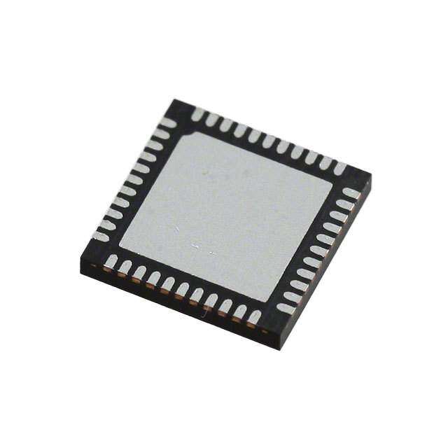
ICGOO电子元器件商城为您提供MAX2010ETI+由Maxim设计生产,在icgoo商城现货销售,并且可以通过原厂、代理商等渠道进行代购。 MAX2010ETI+价格参考。MaximMAX2010ETI+封装/规格:RF 其它 IC 和模块, RF IC RF Predistorter CDMA2000, GSM/EDGE 500MHz ~ 1.1GHz Up to 12dB ACPR Improvement 28-TQFN (5x5)。您可以下载MAX2010ETI+参考资料、Datasheet数据手册功能说明书,资料中有MAX2010ETI+ 详细功能的应用电路图电压和使用方法及教程。
Maxim Integrated的MAX2010ETI+是一款RF系统级封装(SiP)模块,广泛应用于需要高性能射频接收和处理的通信系统中。该器件主要面向450 MHz至4000 MHz的高频段,适用于无线基础设施、微波回传、测试设备、军事通信以及工业控制系统等场景。

MAX2010ETI+集成了下变频混频器、可变增益放大器(VGA)、滤波器和ADC驱动功能,能够将高频RF信号转换为中频(IF)信号,并提供可调增益和出色的线性性能,适合用于多频段、多标准无线接收机设计。其高集成度减少了外围元件需求,简化了系统设计,提高了可靠性。

在具体应用中,该模块常用于软件定义无线电(SDR)、基站收发信机、点对点微波通信、频谱分析仪、信号监测设备等高性能射频接收系统中。此外,由于其良好的温度稳定性和抗干扰能力,也适用于环境复杂、可靠性要求高的工业和军事通信设备。

综上,MAX2010ETI+是一款面向高性能射频接收应用的集成模块,适用于多种高频通信系统,具备高集成度、宽频带、优异性能等特点。
| 参数 | 数值 |
| 产品目录 | |
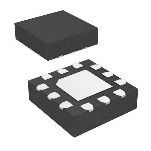
| 描述 | IC RF PREDISTORT ADJ 28-TQFN射频前端 0.5-1.1GHz Adj RF Predistorter |
| 产品分类 | |
| 品牌 | Maxim Integrated |
| 产品手册 | |
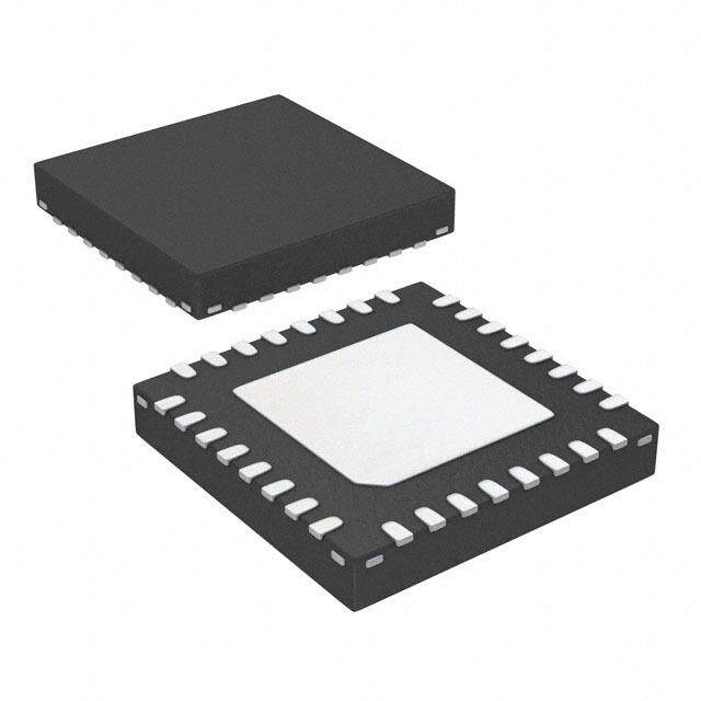
| 产品图片 |
|
| rohs | 符合RoHS无铅 / 符合限制有害物质指令(RoHS)规范要求 |
| 产品系列 | RF集成电路,射频前端,Maxim Integrated MAX2010ETI+- |
| 数据手册 | |
| 产品型号 | MAX2010ETI+ |
| RF类型 | CDMA2000,GSM/EDGE |
| 产品培训模块 | http://www.digikey.cn/PTM/IndividualPTM.page?site=cn&lang=zhs&ptm=25703http://www.digikey.cn/PTM/IndividualPTM.page?site=cn&lang=zhs&ptm=25705 |
| 产品种类 | 射频前端 |
| 供应商器件封装 | 28-TQFN (5x5) |
| 功能 | RF 前置补偿器 |
| 包装 | 管件 |
| 商标 | Maxim Integrated |
| 噪声系数 | 5.5 dB |
| 安装风格 | SMD/SMT |
| 封装 | Tube |
| 封装/外壳 | 28-WFQFN 裸露焊盘 |
| 封装/箱体 | TQFN-EP-28 |
| 工作电源电压 | 4.75 V to 5.25 V |
| 工作频率 | 500 MHz to 1100 MHz |
| 工厂包装数量 | 60 |
| 应用说明 | 点击此处下载产品Datasheet点击此处下载产品Datasheet点击此处下载产品Datasheet点击此处下载产品Datasheet |
| 最大工作温度 | + 85 C |
| 最小工作温度 | - 40 C |
| 标准包装 | 1 |
| 电源电流 | 5.8 mA |
| 系列 | MAX2010 |
| 辅助属性 | 高达 12dB ACPR 性能改善 |
| 零件号别名 | MAX2010 |
| 频率 | 500MHz ~ 1.1GHz |

.jpg)


- 商务部:美国ITC正式对集成电路等产品启动337调查
- 曝三星4nm工艺存在良率问题 高通将骁龙8 Gen1或转产台积电
- 太阳诱电将投资9.5亿元在常州建新厂生产MLCC 预计2023年完工
- 英特尔发布欧洲新工厂建设计划 深化IDM 2.0 战略
- 台积电先进制程称霸业界 有大客户加持明年业绩稳了
- 达到5530亿美元!SIA预计今年全球半导体销售额将创下新高
- 英特尔拟将自动驾驶子公司Mobileye上市 估值或超500亿美元
- 三星加码芯片和SET,合并消费电子和移动部门,撤换高东真等 CEO
- 三星电子宣布重大人事变动 还合并消费电子和移动部门
- 海关总署:前11个月进口集成电路产品价值2.52万亿元 增长14.8%


PDF Datasheet 数据手册内容提取
19-2930; Rev 0; 8/03 500MHz to 1100MHz Adjustable RF Predistorter General Description Features M The MAX2010 adjustable RF predistorter is designed to (cid:2) Up to 12dB ACPR Improvement* A improve power amplifier (PA) adjacent-channel power (cid:2) Independent Gain and Phase Expansion Controls X rejection (ACPR) by introducing gain and phase expan- sion in a PA chain to compensate for the PA’s gain and (cid:2) Gain Expansion Up to 6dB 2 phase compression. With its +23dBm maximum input (cid:2) Phase Expansion Up to 21° 0 power level and wide adjustable range, the MAX2010 (cid:2) 500MHz to 1100MHz Frequency Range 1 can provide up to 12dB of ACPR improvement for (cid:2) Exceptional Gain and Phase Flatness 0 power amplifiers operating in the 500MHz to 1100MHz frequency band. Higher frequencies of operation can (cid:2) Group Delay <2.4ns (Gain and Phase Sections be achieved with this IC’s counterpart, the MAX2009. Combined) The MAX2010 is unique in that it provides up to 6dB of (cid:2) ±0.03ns Group Delay Ripple Over a 100MHz Band gain expansion and 21°of phase expansion as the input (cid:2) Capable of Handling Input Drives Up to +23dBm power is increased. The amount of expansion is config- (cid:2) On-Chip Temperature Variation Compensation urable through two independent sets of control: one set adjusts the gain expansion breakpoint and slope, while (cid:2) Single +5V Supply the second set controls the same parameters for phase. (cid:2) Low Power Consumption: 75mW (typ) With these settings in place, the linearization circuit can (cid:2) Fully Integrated into Small 28-Pin Thin QFN be run in either a static set-and-forget mode, or a more Package sophisticated closed-loop implementation can be *Performance dependent on amplifier, bias, and modulation. employed with real-time software-controlled distortion correction. Hybrid correction modes are also possible Ordering Information using simple lookup tables to compensate for factors such as PA temperature drift or PA loading. PART TEMP RANGE PIN-PACKAGE The MAX2010 comes in a 28-pin thin QFN exposed MAX2010ETI-T -40°C to +85°C 28 Thin QFN-EP* pad (EP) package (5mm x 5mm) and is specified for *EP = Exposed paddle. the extended (-40°C to +85°C) temperature range. Applications Functional Diagram/ Pin Configuration cdma2000™, GSM/EDGE, and iDEN Base Stations Feed-Forward PA Architectures ND* UTG ND* CS FS BP ND* G O G G G G G Digital Baseband Predistortion Architectures 28 27 26 25 24 23 22 Military Applications GND* 1 21 VCCG GAIN GND* 2 CONTROL 20 GND* ING 3 19 PBRAW GND* 4 18 PBEXP MAX2010 GND* 5 17 PBIN OUTP 6 PHASE 16 GND* CONTROL GND* 7 15 VCCP 8 9 10 11 12 13 14 D* NP D* S1 S2 S1 S2 cdma2000 is a trademark of Telecommunications Industry GN I GN PF PF DC DC P P Assoc. *INTERNALLY CONNECTED TO EXPOSED GROUND PADDLE. ________________________________________________________________Maxim Integrated Products 1 For pricing, delivery, and ordering information,please contact Maxim/Dallas Direct!at 1-888-629-4642, or visit Maxim’s website at www.maxim-ic.com.
500MHz to 1100MHz Adjustable RF Predistorter 0 ABSOLUTE MAXIMUM RATINGS 1 VCCG, VCCPto GND..............................................-0.3V to +5.5V Continuous Power Dissipation (TA= +70°C) 0 ING, OUTG, GCS, GFS, GBP to GND......-0.3V to (VCCG+ 0.3V) 28-Pin Thin QFN-EP INP, OUTP, PFS_, PDCS_, PBRAW, (derate 21mW/°C above +70°C)...............................1667mW 2 PBEXP, PBIN to GND............................-0.3V to (VCCP+ 0.3V) Operating Temperature Range...........................-40°C to +85°C X Input (ING, INP, OUTP, OUTG) Level............................+23dBm Junction Temperature......................................................+150°C PBEXP Output Current........................................................±1mA Storage Temperature Range.............................-65°C to +150°C A Lead Temperature (soldering 10s)..................................+300°C M Stresses beyond those listed under “Absolute Maximum Ratings” may cause permanent damage to the device. These are stress ratings only, and functional operation of the device at these or any other conditions beyond those indicated in the operational sections of the specifications is not implied. Exposure to absolute maximum rating conditions for extended periods may affect device reliability. DC ELECTRICAL CHARACTERISTICS (MAX2010 EV kit; VCCG= VCCP= +4.75V to +5.25V; no RF signal applied; INP, ING, OUTP, OUTG are AC-coupled and terminated to 50Ω. VPF_S1= open; PBEXP shorted to PBRAW; VPDCS1= VPDCS2= 0.8V; VPBIN= VGBP= VGCS= GND; VGFS= VCCG;TA= -40°C to +85°C. Typical values are at VCCG= VCCP= +5.0V, TA= +25°C, unless otherwise noted.) PARAMETER CONDITIONS MIN TYP MAX UNITS Supply Voltage VCCG, VCCP 4.75 5.25 V VCCP 5.8 7 Supply Current mA VCCG 10 12.1 PBIN, PBRAW 0 VCCP Analog Input Voltage Range V GBP, GFS, GCS 0 VCCG VGFS = VGCS = VPBRAW = 0V -2 +2 Analog Input Current VGBP = 0 to +5V -100 +170 µA VPBIN = 0 to +5V -100 +220 Logic-Input High Voltage PDCS1, PDCS2 (Note 1) 2.0 V Logic-Input Low Voltage PDCS1, PDCS2 (Note 1) 0.8 V Logic Input Current -2 +2 µA 2 _______________________________________________________________________________________
500MHz to 1100MHz Adjustable RF Predistorter AC ELECTRICAL CHARACTERISTICS M (MAX2010 EV kit, VCCG = VCCP = +4.75V to +5.25V, 50Ω environment, PIN = -20dBm, fIN = 500MHz to 1100MHz, VGCS = +1.0V, A VGFS= +5.0V, VGBP= +1.2V, VPBIN= VPDCS1= VPDCS2= 0V, VPF_S1= +5V, VPBRAW= VPBEXP,TA= -40°C to +85°C. Typical val- ues are at fIN= 880MHz, VCCG= VCCP= +5V, TA= +25°C, unless otherwise noted.) (Notes 1, 2) X 2 PARAMETER CONDITIONS MIN TYP MAX UNITS 0 Operating Frequency Range 500 1100 MHz 1 VSWR ING, INP, OUTG, OUTP 1.3:1 0 PHASE CONTROL SECTION Nominal Gain -5.5 dB Gain Variation Over Temperature TA = -40°C to +85°C -1.7 dB Gain Flatness Over a 100MHz band ±0.1 dB Phase-Expansion Breakpoint VPBIN = +5V 23 dBm Maximum Phase-Expansion Breakpoint VPBIN = 0V 0.7 dBm Minimum Phase-Expansion Breakpoint TA = -40°C to +85°C ±1.5 dB Variation Over Temperature VPF_S1 = +5V, VPDCS1 = VPDCS2 = 0V, 21 PIN = -20 dBm to +23 dBm VPDCS1 = 5V, VPDCS2 = 0V, 16 VPF_S1 = +1.5V Phase Expansion Degrees VPDCS1 = 0V, VPDCS2 = 5V, 14 VPF_S1 = +1.5V VPF_S1 = 0V, VPDCS1 = VPDCS2 = +5V, 6 PIN = -20dBm to +23dBm Phase-Expansion Slope Degrees PIN = +9dBm 1.4 Maximum /dB VPF_S1 = 0V, Degrees Phase-Expansion Slope Minimum VPDCS1 = VPDCS2 = +5V, 0.6 /dB PIN = +9dBm Phase-Slope Variation Over Degrees PIN = +9dBm, TA = -40°C to +85°C 0.05 Temperature /dB Phase Ripple Over a 100MHz band, deviation from linear phase ±0.02 Degrees Noise Figure 5.5 dB Absolute Group Delay Interconnects de-embedded 1.3 ns Group Delay Ripple Over a 100MHz band ±0.01 ns Parasitic Gain Expansion PIN = -20dBm to +23dBm +0.4 dB _______________________________________________________________________________________ 3
500MHz to 1100MHz Adjustable RF Predistorter 0 AC ELECTRICAL CHARACTERISTICS (continued) 1 (MAX2010 EV kit, VCCG = VCCP = +4.75V to +5.25V, 50Ω environment, PIN = -20dBm, fIN = 500MHz to 1100MHz, VGCS = +1.0V, 0 VGFS= +5.0V, VGBP= +1.2V, VPBIN= VPDCS1= VPDCS2= 0V, VPF_S1= +5V, VPBRAW= VPBEXP,TA= -40°C to +85°C. Typical val- 2 ues are at fIN= 880MHz, VCCG= VCCP= +5V, TA= +25°C, unless otherwise noted.) (Notes 1, 2) X PARAMETER CONDITIONS MIN TYP MAX UNITS A GAIN CONTROL SECTION -14.9 M Nominal Gain VGCS = 0V, VGFS = +5V -24.3 dB VGCS = +5V, VGFS = 0V -7.6 Gain Variation Over Temperature TA = -40°C to +85°C -1.4 dB Gain Flatness Over a 100MHz band ±0.2 dB Gain-Expansion Breakpoint VGBP = +5V 23 dBm Maximum Gain-Expansion Breakpoint VGBP = +0.5V -2.5 dBm Minimum Gain-Expansion Breakpoint TA = -40°C to +85°C -0.5 dB Variation Over Temperature VGFS = +5V, PIN = -20dBm to +23dBm 5.3 Gain-Expansion dB VGFS = 0V, PIN = -20dBm to +23dBm 3.1 VGFS = +5V, PIN = +15dBm 0.43 Gain-Expansion Slope dB/dB VGFS = +0V, PIN = +15dBm 0.23 Gain-Slope Variation Over PIN = +15dBm, TA = -40°C to +85°C -0.01 dB/dB Temperature Noise Figure 14.9 dB Absolute Group Delay Interconnects de-embedded 1.12 ns Group Delay Ripple Over a 100MHz band ±0.02 ns Phase Ripple Over a 100MHz band, deviation from linear phase ±0.09 Degrees Parasitic Phase Expansion PIN = -20dBm to +23dBm +3 Degrees Note 1: Guaranteed by design and characterization. Note 2: All limits reflect losses and characteristics of external components shown in the Typical Application Circuit, unless otherwise noted. 4 _______________________________________________________________________________________
500MHz to 1100MHz Adjustable RF Predistorter Typical Operating Characteristics M Phase Control Section A (MAX2010 EV kit, VCCP= +5.0V, PIN= -20dBm, VPBIN= 0V, VPF_S1 = +5.0V, VPDCS1= VPDCS2= 0V, fIN= 880MHz, TA= +25°C X unless otherwise noted.) 2 SUPPLY CURRENT SMALL-SIGNAL INPUT RETURN LOSS SMALL-SIGNAL OUTPUT RETURN LOSS 0 vs. SUPPLY VOLTAGE vs. FREQUENCY vs. FREQUENCY 1 666...456 MAX2010 toc01 100 MAX2010 toc02 100 MAX2010 toc03 0 SUPPLY CURRENT (mA) 556666......980123 TA = +85°C TA = +T2A5 =° C-40°C INPUT RETURN LOSS (dB) 423000 D C OUTPUT RETURN LOSS (dB) 423000 A D BC 5.7 B A 5.6 50 50 4.75 4.85 4.95 5.05 5.15 5.25 0.5 0.6 0.7 0.8 0.9 1.0 1.1 0.5 0.6 0.7 0.8 0.9 1.0 1.1 SUPPLY VOLTAGE (V) FREQUENCY (GHz) FREQUENCY (GHz) A = VPDCS1 = VPDCS2 = VPF_S1 = 0V A = VPDCS1 = VPDCS2 = VPF_S1 = 0V B = VPDCS1 = VPDCS2 = 0V, VPF_S1 = 5V B = VPDCS1 = VPDCS2 = 0V, VPF_S1 = 5V C = VPDCS1 = VPDCS2 = 5V, VPF_S1 = 0V C = VPDCS1 = VPDCS2 = 5V, VPF_S1 = 0V D = VPDCS1 = VPDCS2 = VPF_S1 = 5V D = VPDCS1 = VPDCS2 = VPF_S1 = 5V LARGE-SIGNAL INPUT RETURN LOSS LARGE-SIGNAL OUTPUT RETURN LOSS SMALL-SIGNAL GAIN vs. FREQUENCY vs. FREQUENCY vs. FREQUENCY 100 MAX2010 toc04 100 MAX2010 toc05 --44..50 MAX2010 toc06 S (dB) B A SS (dB) B A -5.0 TA = -40°C T RETURN LOS 2300 UT RETURN LO 2300 D C GAIN (dB) --65..05 TTAA = = + +8255°°CC PU D TP N U I 40 O 40 -6.5 C 50 50 -7.0 0.5 0.6 0.7 0.8 0.9 1.0 1.1 0.5 0.6 0.7 0.8 0.9 1.0 1.1 0.5 0.6 0.7 0.8 0.9 1.0 1.1 FREQUENCY (GHz) FREQUENCY (GHz) FREQUENCY (GHz) PIN = +15dBm PIN = +15dBm A = VPDCS1 = VPDCS2 = VPF_S1 = 0V A = VPDCS1 = VPDCS2 = VPF_S1 = 0V B = VPDCS1 = VPDCS2 = 0V, VPF_S1 = 5V B = VPDCS1 = VPDCS2 = 0V, VPF_S1 = 5V C = VPDCS1 = VPDCS2 = 5V, VPF_S1 = 0V C = VPDCS1 = VPDCS2 = 5V, VPF_S1 = 0V D = VPDCS1 = VPDCS2 = VPF_S1 = 5V D = VPDCS1 = VPDCS2 = VPF_S1 = 5V _______________________________________________________________________________________ 5
500MHz to 1100MHz Adjustable RF Predistorter 0 Typical Operating Characteristics (continued) 1 Phase Control Section (continued) 0 2 (MAX2010 EV kit, VCCP= +5.0V, PIN= -20dBm, VPBIN= 0V, VPF_S1 = +5.0V, VPDCS1= VPDCS2= 0V, fIN= 880MHz, TA= +25°C unless otherwise noted.) X A SMALL-SIGNAL GAIN SMALL-SIGNAL GAIN SMALL-SIGNAL GAIN vs. FREQUENCY vs. COARSE SLOPE vs. COARSE SLOPE M -4.0 -4.0 -4.0 -4.5 MAX2010 toc07 -4.5 VPF_S1 = 1.5V VPF_S1 = 0V MAX2010 toc08 -4.5 TA = -40°C MAX2010 toc09 -5.0 -5.0 -5.0 TA = +25°C N (dB) -5.5 VCCP = 4.75V, 5.0V, 5.25V N (dB) -5.5 N (dB) -5.5 TA = +85°C AI AI AI G G VPF_S1 = 5V G -6.0 -6.0 -6.0 -6.5 -6.5 -6.5 -7.0 -7.0 -7.0 0.5 0.6 0.7 0.8 0.9 1.0 1.1 PDCS1 = 0 PDCS1 = 5 PDCS1 = 0 PDCS1 = 5 PDCS1 = 0 PDCS1 = 5 PDCS1 = 0 PDCS1 = 5 FREQUENCY (GHz) PDCS2 = 0 PDCS2 = 0 PDCS2 = 5 PDCS2 = 5 PDCS2 = 0 PDCS2 = 0 PDCS2 = 5 PDCS2 = 5 COARSE SLOPE (V) COARSE SLOPE (V) GROUP DELAY vs. FREQUENCY NOISE FIGURE vs. FREQUENCY SUPPLY CURRENT vs. INPUT POWER 11..4550 MAX2010 toc10 667...680 MAX2010 toc11 56..9050 MAX2010 toc12 A) B DELAY (ns) 111...334050 C A NOISE FIGURE (dB) 55666.....68024 D B SUPPLY CURRENT (m555...889050 A CD 1.25 5.4 5.75 5.2 E D B A C 1.20 5.0 5.70 0.5 0.6 0.7 0.8 0.9 1.0 1.1 0.5 0.6 0.7 0.8 0.9 1.0 1.1 0 4 8 12 16 20 24 FREQUENCY (GHz) FREQUENCY (GHz) INPUT POWER (dBm) A = VPDCS1 = VPDCS2 = VPF_S1 = 0V A = VPDCS1 = VPDCS2 = VPF_S1 = 0V A = VPBIN = 0V D = VPBIN = 1.5V B = VPDCS1 = VPDCS2 = 0V, VPF_S1 = 5V B = VPDCS1 = VPDCS2 = 0V, VPF_S1 = 5V B = VPBIN = 0.5V E = VPBIN = 3.0V C = VPDCS1 = VPDCS2 = 5V, VPF_S1 = 0V C = VPDCS1 = VPDCS2 = 5V, VPF_S1 = 0V C = VPBIN = 1.0V D = VPDCS1 = VPDCS2 = VPF_S1 = 5V D = VPDCS1 = VPDCS2 = VPF_S1 = 5V INTERCONNECTS DE-EMBEDDED 6 _______________________________________________________________________________________
500MHz to 1100MHz Adjustable RF Predistorter Typical Operating Characteristics (continued) M Phase Control Section (continued) A (MAX2010 EV kit, VCCP= +5.0V, PIN= -20dBm, VPBIN= 0V, VPF_S1 = +5.0V, VPDCS1= VPDCS2= 0V, fIN= 880MHz, TA= +25°C X unless otherwise noted.) 2 0 GAIN EXPANSION vs. INPUT POWER PHASE EXPANSION vs. INPUT POWER GAIN EXPANSION vs. INPUT POWER 1 --44..75 D E F MAX2010 toc13 1105 C MAX2010 toc14 --44..75 MAX2010 toc15 0 5 -4.9 S) B -4.9 GAIN (dB)-5.1 CB ASE (DEGREE -50 A GAIN (dB)-5.1 A BC -5.3 H -5.3 A P -10 D D -5.5 E -5.5 -15 -5.7 F -5.7 -7 -2 3 8 13 18 23 -20 -7 -2 3 8 13 18 23 -7 -2 3 8 13 18 23 INPUT POWER (dBm) INPUT POWER (dBm) A = VPBIN = 0V D = VPBIN = 1.5V INPUT POWER (dBm) A = VPDCS1 = VPDCS2 = 0V C = VPDCS1 = 0V, VPDCS2 = 5V B = VPBIN = 0.5V E = VPBIN = 2.0V A = VPBIN = 0V D = VPBIN = 1.5V B = VPDCS1 = 5V, VPDCS2 = 0V D = VPDCS1 = VPDCS2 = 5V C = VPBIN = 1.0V F = VPBIN = 2.5V B = VPBIN = 0.5V E = VPBIN = 2.0V C = VPBIN = 1.0V F = VPBIN = 2.5V GAIN EXPANSION vs. INPUT POWER PHASE EXPANSION vs. INPUT POWER PHASE EXPANSION vs. INPUT POWER -4.5 MAX2010 toc16 1105 F MAX2010 toc17 1105 MAX2010 toc18 -4.8 5 5 S) S) EE E EE B GAIN (dB)-5.1 SE (DEGR -50 D SE (DEGR -50 A D C B PHA PHA D E -10 -10 -5.4 F B A C -15 -15 A C -5.7 -20 -20 -7 -2 3 8 13 18 23 -7 -2 3 8 13 18 23 -7 -2 3 8 13 18 23 INPUT POWER (dBm) INPUT POWER (dBm) INPUT POWER (dBm) A = VPF_S1 = 0V E = VPF_S1 = 2.0V A = VPF_S1 = 0V D = VPF_S1 = 1.5V A = VPDCS1 = VPDCS2 = 0V B = VPF_S1 = 0.5V F = VPF_S1 = 5.0V B = VPF_S1 = 0.5V E = VPF_S1 = 2.0V B = VPDCS1 = 5V, VPDCS2 = 0V C = VPF_S1 = 1.0V VPDCS1 = 5.0V C = VPF_S1 = 1.0V F = VPF_S1 = 5.0V C = VPDCS1 = 0V, VPDCS2 = 5V D = VPF_S1 = 1.5V VPDCS1 = 5.0V D = VPDCS1 = VPDCS2 = 5V _______________________________________________________________________________________ 7
500MHz to 1100MHz Adjustable RF Predistorter 0 Typical Operating Characteristics (continued) 1 Phase Control Section (continued) 0 (MAX2010 EV kit, VCCP= +5.0V, PIN= -20dBm, VPBIN= 0V, VPF_S1 = +5.0V, VPDCS1= VPDCS2= 0V, fIN= 880MHz, TA= +25°C 2 unless otherwise noted.) X A GAIN EXPANSION vs. INPUT POWER PHASE EXPANSION vs. INPUT POWER M ---444...420 VPDCS1 = 5.0, VPF_S1 = 1.5V MAX2010 toc19 -05 VPDCS1 = 5.0, VPF_S1 = 1.5V MAX2010 toc20 -4.6 TA = -40°C ES) GAIN (dB) --54..08 TA = +25°C SE (DEGRE -10 TA = +25°C A -15 -5.2 PH TA = +85°C -5.4 TA = +85°C -20 TA = -40°C -5.6 -5.8 -25 -7 -2 3 8 13 18 23 -7 -2 3 8 13 18 23 INPUT POWER (dBm) INPUT POWER (dBm) Typical Operating Characteristics Gain Control Section (MAX2010 EV kit, VCCG= +5.0V, PIN= -20dBm, VGBP= +1.2V, VGFS= +5.0V, VGCS= +1.0V, fIN= 880MHz, TA= +25°C, unless otherwise noted.) SMALL-SIGNAL INPUT RETURN LOSS SMALL-SIGNAL OUTPUT RETURN LOSS SUPPLY CURRENT vs. SUPPLY VOLTAGE vs. FREQUENCY vs. FREQUENCY SUPPLY CURRENT (mA) 66566666........65914320 TA = +8T5A° =C +25°C TA = -40°C MAX2010 toc21 INPUT RETURN LOSS (dB) 3210000 A, B C, D MAX2010 toc22 OUTPUT RETURN LOSS (dB) 3210000 A, B C, D MAX2010 toc23 5.8 40 40 5.7 5.6 50 50 4.75 4.85 4.95 5.05 5.15 5.25 0.5 0.6 0.7 0.8 0.9 1.0 1.1 0.5 0.6 0.7 0.8 0.9 1.0 1.1 SUPPLY VOLTAGE (V) FREQUENCY (GHz) FREQUENCY (GHz) A = VGCS = 0V, VGFS = 0V C = VGCS = 5V, VGFS = 0V A = VGCS = 0V, VGFS = 0V C = VGCS = 5V, VGFS = 0V B = VGCS = 0V, VGFS = 5V D = VGCS = 5V, VGFS = 5V B = VGCS = 0V, VGFS = 5V D = VGCS = 5V, VGFS = 5V 8 _______________________________________________________________________________________
500MHz to 1100MHz Adjustable RF Predistorter Typical Operating Characteristics (continued) M Gain Control Section (continued) A (MAX2010 EV kit, VCCP= +5.0V, PIN= -20dBm, VPBIN= 0V, VPF_S1 = +5.0V, VPDCS1= VPDCS2= 0V, fIN= 880MHz, TA= +25°C X unless otherwise noted.) 2 LARGE-SIGNAL INPUT RETURN LOSS LARGE-SIGNAL OUTPUT RETURN LOSS 0 vs. FREQUENCY vs. FREQUENCY SMALL-SIGNAL GAIN vs. FREQUENCY 1 INPUT RETURN LOSS (dB) 3210000 PIN = +A15dBm D C MAX2010 toc24 OUTPUT RETURN LOSS (dB) 3210000 PIN = +1A5dBm D C B MAX2010 toc25 GAIN (dB) -------11111118674352 TA = +85°C TAT =A +=2 -54°0C°C MAX2010 toc26 0 40 B 40 -19 50 50 -20 0.5 0.6 0.7 0.8 0.9 1.0 1.1 0.5 0.6 0.7 0.8 0.9 1.0 1.1 0.5 0.6 0.7 0.8 0.9 1.0 1.1 FREQUENCY (GHz) FREQUENCY (GHz) FREQUENCY (GHz) A = VGCS = 0V, VGFS = 0V C = VGCS = 5V, VGFS = 0V A = VGCS = 0V, VGFS = 0V C = VGCS = 5V, VGFS = 0V B = VGCS = 0V, VGFS = 5V D = VGCS = 5V, VGFS = 5V B = VGCS = 0V, VGFS = 5V D = VGCS = 5V, VGFS = 5V SMALL-SIGNAL GAIN vs. FREQUENCY SMALL-SIGNAL GAIN vs. VGCS SMALL-SIGNAL GAIN vs. VGCS --1132 VCCG = 4.75V, 5.0V, 5.25V MAX2010 toc27 -05 VGFS = 0V, 1.5V, 5.0V MAX2010 toc28 -05 TA = -40°C MAX2010 toc29 -14 -10 -10 GAIN (dB) --1165 GAIN (dB) -15 GAIN (dB) -15 TA = +25°C TA = +85°C -17 -20 -20 -18 -25 -25 -19 VGFS = +1.5V -20 -30 -30 0.5 0.6 0.7 0.8 0.9 1.0 1.1 0 1 2 3 4 5 0 1 2 3 4 5 FREQUENCY (GHz) VGCS (V) VGCS (V) _______________________________________________________________________________________ 9
500MHz to 1100MHz Adjustable RF Predistorter 0 Typical Operating Characteristics (continued) 1 Gain Control Section (continued) 0 (MAX2010 EV kit, VCCP= +5.0V, PIN= -20dBm, VPBIN= 0V, VPF_S1 = +5.0V, VPDCS1= VPDCS2= 0V, fIN= 880MHz, TA= +25°C 2 unless otherwise noted.) X A GROUP DELAY vs. FREQUENCY NOISE FIGURE vs. FREQUENCY SUPPLY CURRENT vs. INPUT POWER M 11..45 MAX2010 toc30 2350 A MAX2010 toc31 2350 MAX2010 toc32 B 1.3 A) DELAY (ns) 11..12 C, D A OISE FIGURE (dB) 1250 B C PLY CURRENT (m 2105 C A N P 1.0 SU E 10 10 E 0.9 D B D 0.8 5 5 0.5 0.6 0.7 0.8 0.9 1.0 1.1 0.5 0.6 0.7 0.8 0.9 1.0 1.1 0 4 8 12 16 20 24 FREQUENCY (GHz) FREQUENCY (GHz) INPUT POWER (dBm) A = VGCS = 0V, VGFS = 0V C = VGCS = 5V, VGFS = 0V A = VGCS = 0V, VGFS = 0V D = VGCS = 5V, VGFS = 0V A = VGBP = 0V D = VGBP = 1.5V B = VGCS = 0V, VGFS = 5V D = VGCS = 5V, VGFS = 5V B = VGCS = 0V, VGFS = 5V E = VGCS = 5V, VGFS = 5V B = VGBP = 0.5V E = VGBP = 3.0V INTERCONNECTS DE-EMBEDDED C = VGCS = 1.5V, VGFS = 5V C = VGBP = 1.0V GAIN EXPANSION vs. INPUT POWER PHASE EXPANSION vs. INPUT POWER -5 -5 -8 B C MAX2010 toc33 -7 B MAX2010 toc34 A E GAIN (dB) --1114 A D ASE (DEGREES) -1-91 C H P D G F -17 F H -13 H G E -20 -15 -7 -2 3 8 13 18 23 -7 -2 3 8 13 18 23 INPUT POWER (dBm) INPUT POWER (dBm) A = VGBP = 0V E = VGBP = 2.0V A = VGBP = 0V E = VGBP = 2.0V B = VGBP = 0.5V F = VGBP = 2.5V B = VGBP = 0.5V F = VGBP = 2.5V C = VGBP = 1.0V G = VGBP = 3.5V C = VGBP = 1.0V G = VGBP = 3.5V D = VGBP = 1.5V H = VGBP = 5.0V D = VGBP = 1.5V H = VGBP = 5.0V 10 ______________________________________________________________________________________
500MHz to 1100MHz Adjustable RF Predistorter Typical Operating Characteristics (continued) M Gain Control Section (continued) A (MAX2010 EV kit, VCCP= +5.0V, PIN= -20dBm, VPBIN= 0V, VPF_S1 = +5.0V, VPDCS1= VPDCS2= 0V, fIN= 880MHz, TA= +25°C X unless otherwise noted.) 2 0 GAIN EXPANSION vs. INPUT POWER GAIN EXPANSION vs. INPUT POWER PHASE EXPANSION vs. INPUT POWER -5 -5 30 1 -8 E MAX2010 toc35 --79 F E MAX2010 toc36 20 MAX2010 toc37 0 F -11 A, B S) GAIN (dB) --1114 C D A, B GAIN (dB) ----11113759 D C PHASE (DEGREE 100 C E A, B D -17 -21 -10 -23 F -20 -25 -20 -7 -2 3 8 13 18 23 -7 -2 3 8 13 18 23 -7 -2 3 8 13 18 23 INPUT POWER (dBm) INPUT POWER (dBm) INPUT POWER (dBm) A = VGFS = 0V D = VGFS = 1.5V A = VGCS = 0V D = VGCS = 1.5V A = VGCS = 0V D = VGCS = 1.5V B = VGFS = 0.5V E = VGFS = 2.0V B = VGCS = 0.5V E = VGCS = 2.0V B = VGCS = 0.5V E = VGCS = 2.0V C = VGFS = 1.0V F = VGFS = 5.0V C = VGCS = 1.0V F = VGCS = 2.5V C = VGCS = 1.0V F = VGCS = 5.0V PHASE EXPANSION vs. INPUT POWER GAIN EXPANSION vs. INPUT POWER PHASE EXPANSION vs. INPUT POWER -5 -8 -5 --76 F MAX2010 toc38 -1-90 MAX2010 toc39 --67 MAX2010 toc40 E -8 -8 S) -11 S) PHASE (DEGREE ---111-0129 C D GAIN (dB) ---111432 TTAA == +-4205°°CC PHASE (DEGREE ---111-2091 TTAA == -+4205°°CC -13 A, B -15 TA = +85°C -13 TA = +85°C -14 -16 -14 -15 -17 -15 -7 -2 3 8 13 18 23 -7 -2 3 8 13 18 23 -7 -2 3 8 13 18 23 INPUT POWER (dBm) INPUT POWER (dBm) INPUT POWER (dBm) A = VGFS = 0V D = VGFS = 1.5V B = VGFS = 0.5V E = VGFS = 2.0V C = VGFS = 1.0V F = VGFS = 5.0V ______________________________________________________________________________________ 11
500MHz to 1100MHz Adjustable RF Predistorter 0 Pin Description 1 0 PIN NAME FUNCTION 2 1, 2, 4, 5, 7, X 8, 10, 16, 20, GND Ground. Internally connected to the exposed paddle. 22, 26, 28 A RF Gain Input. Connect ING to a coupling capacitor if it is not connected to OUTP. ING is M 3 ING interchangeable with OUTG. RF Phase Output. Connect OUTP to a coupling capacitor if it is not connected to INP. OUTP is 6 OUTP interchangeable with INP. 9 INP RF Phase Input. Connect INP to a coupling capacitor. This pin is interchangeable with OUTP. 11 PFS1 Fine Phase-Slope Control Input 1. See the Typical Application Circuit. 12 PFS2 Fine Phase-Slope Control Input 2. See the Typical Application Circuit. 13 PDCS1 Digital Coarse Phase-Slope Control Range Input 1. Set to logical zero for the steepest slope. 14 PDCS2 Digital Coarse Phase-Slope Control Range Input 2. Set to logical zero for the steepest slope. Phase-Control Supply Voltage. Bypass with a 0.01µF capacitor to ground as close to the device as 15 VCCP possible. Phase section can operate without VCCG. 17 PBIN Phase Breakpoint Control Input 18 PBEXP Phase Expansion Output. Connect PBEXP to PBRAW to use PBIN as the breakpoint control voltage. 19 PBRAW Uncompensated Phase Breakpoint Input Gain-Control Supply Voltage. Bypass with a 0.01µF capacitor to ground as close to the device as 21 VCCG possible. Gain section can operate without VCCP. 23 GBP Gain Breakpoint Control Input 24 GFS Fine Gain-Slope Control Input 25 GCS Coarse Gain-Slope Control Input 27 OUTG RF Gain Output. Connect OUTG to a coupling capacitor. OUTG is interchangeable with ING. EP GND Exposed Ground Paddle. Solder EP to the ground plane. Detailed Description phase breakpoints can be set over a 20dB input power range. The phase expansion slope is variable from The MAX2010 adjustable predistorter can provide up to 0.3°/dB to 2.0°/dB and can be adjusted for a maximum 12dB of ACPR improvement for high-power amplifiers of 21°of phase expansion. The gain expansion slope is by introducing gain and phase expansion to compen- variable from 0.1dB/dB to 0.53dB/dB and can be sate for the PA’s gain and phase compression. The adjusted for a maximum of 6dB gain expansion. MAX2010 enables real-time software-controlled distor- tion correction, as well as set-and-forget tuning through The following sections describe the tuning methodology the adjustment of the expansion starting point (break- best implemented with a class A amplifier. Other classes point) and the rate of expansion (slope). The gain and of operation may require significantly different settings. 12 ______________________________________________________________________________________
500MHz to 1100MHz Adjustable RF Predistorter Phase Expansion Circuitry the PFS1 and PFS2 pins perform the task of fine tuning M Figure 1 shows a typical PA’s phase behavior with the phase expansion slope. Since off-chip varactor respect to input power. For input powers less than the diodes are recommended for this function, they must A breakpoint level, the phase remains relatively constant. be closely matched and identically biased. A minimum X As the input power becomes greater than the break- effective capacitance of 2pF to 6pF is required 2 point level, the phase begins to compress and deterio- to achieve the full phase slope range as specified in rate the power amplifier’s linearity. To compensate for the Electrical Characteristics tables. 0 this AM-PM distortion, the MAX2010 provides phase 1 As shown in Figure 2, the varactors connected to PFS1 expansion, which occurs at the same breakpoint level and PFS2 are in series with three internal capacitors on 0 but with the opposite slope. The overall result is a flat each pin. By connecting and disconnecting these inter- phase response. nal capacitors, a larger change in phase expansion Phase Expansion Breakpoint slope can be achieved through the logic levels present- The phase expansion breakpoint is typically controlled ed at the PDCS1 and PDCS2 pins. The phase expan- by a digital-to-analog converter (DAC) connected sion slope is at its maximum when both VPDCS1 and through the PBIN pin. The PBIN input voltage range of VPDCS2 equal 0V. The phase tuning has a minimal 0V to VCC corresponds to a breakpoint input power effect on the small-signal gain. range of 0.7dBm to 23dBm. To achieve optimal perfor- Gain Expansion Circuitry mance, the phase expansion breakpoint of the In addition to phase compression, the PA also suffers MAX2010 must be set to equal the phase compression from gain compression (AM-AM) distortion, as shown in breakpoint of the PA. Figure 3. The PA gain curve remains flat for input pow- Phase Expansion Slope ers below the breakpoint level, and begins to compress The phase expansion slope of the MAX2010 must also at a given rate (slope) for input powers greater than the be adjusted to equal the opposite slope of the PA’s breakpoint level. To compensate for such gain com- phase compression curve. The phase expansion slope pression, the MAX2010 generates a gain expansion, of the MAX2010 is controlled by the PFS1, PFS2, PDCS1, which occurs at the same breakpoint level with the and PDCS2 pins. With pins PFS1 and PFS2 AC-coupled opposite slope. The overall result is a flat gain response and connected to a variable capacitor or varactor diode, at the PA output. PA PHASE MAX2010 IMPROVED COMPRESSION PHASE EXPANSION PHASE DISTORTION BREAKPOINT PA PHASE (DEGREES) SLOPE MAX2010 PHASE (DEGREES) OMBINED PHASE (DEGREES) C PIN (dBm) PIN (dBm) PIN (dBm) Figure 1. PA Phase Compression Canceled by MAX2010 Phase Expansion ______________________________________________________________________________________ 13
500MHz to 1100MHz Adjustable RF Predistorter 0 1 0 2 PFS1 X A M PF_S1 PHASE-CONTROL CIRCUITRY PFS2 2 PDCS1 SWITCH CONTROL MAX2010 PDCS2 Figure 2. Simplified Phase Slope Internal Circuitry PA GAIN MAX2010 IMPROVED COMPRESSION GAIN EXPANSION GAIN DISTORTION BREAKPOINT PA GAIN (dB) SLOPE MAX2010 GAIN (dB) OMBINED GAIN (dB) C PIN (dBm) PIN (dBm) PIN (dBm) Figure 3. PA Gain Compression Canceled by MAX2010 Gain Expansion 14 ______________________________________________________________________________________
500MHz to 1100MHz Adjustable RF Predistorter Gain Expansion Breakpoint Applications Information M The gain expansion breakpoint is usually controlled by The following section describes the tuning methodology a DAC connected through the GBP pin. The GBP input A best implemented with a class A amplifier. Other classes voltage range of 0.5V to 5V corresponds to a break- X of operation may require significantly different settings. point input power range of -2.5dBm to 23dBm. To 2 achieve the optimal performance, the gain expansion Gain and Phase Expansion Optimization breakpoint of the MAX2010 must be set to equal the The best approach to improve the ACPR of a PA is to 0 gain compression point of the PA. The GBP control has first optimize the AM-PM response of the phase sec- 1 a minimal effect on the small-signal gain when operat- tion. For most high-frequency LDMOS amplifiers, 0 ed from 0.5V to 5V. improving the AM-PM response provides the bulk of the ACPR improvement. Figure 4 shows a typical configu- Gain Expansion Slope ration of the phase tuning circuit. A power sweep on a In addition to properly setting the breakpoint, the gain network analyzer allows quick real-time tuning of the expansion slope of the MAX2010 must also be adjusted AM-PM response. First, tune PBIN to achieve the phase to compensate for the PA’s gain compression. The expansion starting point (breakpoint) at the same point slope should be set using the following equation: where the PA’s phase compression begins. Next, use −PA_SLOPE control pins PF_S1, PDCS1, and PDCS2 to obtain the MAX2010_SLOPE= optimal AM-PM response. The typical values for these 1+PA_SLOPE pins are shown in Figure 4. where: To further improve the ACPR, connect the phase out- MAX2010_SLOPE = MAX2010 gain section’s slope in put to the gain input through a preamplifier. The pre- dB/dB. amplifier is used to compensate for the high insertion PA_SLOPE = PA’s gain slope in dB/dB, a negative loss of the gain section. Figure 5 shows a typical appli- number for compressive behavior. cation circuit of the MAX2010 with the phase section cascaded to the gain section for further ACPR opti- To modify the gain expansion slope, two adjustments mization. Similar to tuning the phase section, first tune must be made to the biases applied on pins GCS and the gain expansion breakpoint through the GBP pin GFS. Both GCS and GFS have an input voltage range of and adjust for the desired gain expansion with pins 0V to VCC, corresponding to a slope of approximately GCS and GFS. To minimize the effect of GCS on the 0.1dB/dB to 0.53dB/dB. The slope is set to maximum parasitic phase response, minimize the control voltage when VGCS= 0V and VGFS= +5V, and the slope is at its to around 1V. Some retuning of the AM-PM response minimum when VGCS= +5V and VGFS= 0V. may be necessary. Unlike the GBP pin, modifying the gain expansion slope bias on the GCS pin causes a change in the part’s inser- Layout Considerations tion loss and noise figure. For example, a smaller slope A properly designed PC board is an essential part of any caused by GCS results in a better insertion loss and high-frequency circuit. In order to minimize external com- lower noise figure. The GFS does not affect the insertion ponents, the PC board can be designed to incorporate loss. It can provide up to -30% or +30% total slope varia- small values of inductance and capacitance to optimize tion around the nominal slope set by GCS. the input and output VSWR (refer to the MAX2009/ MAX2010 EV Kit). The phase section’s PFS1 and PFS2 Large amounts of GCS bias adjustment can also lead to pins are sensitive to external parasitics. Minimize trace an undesired (or residual) phase expansion/compres- lengths and keep varactor diodes close to the pins. sion behavior. There exists an optimal bias voltage that Remove the ground plane underneath the traces can fur- minimizes this parasitic behavior (typically GCS = 1.0V). ther help reduce the parasitic capacitance. For best per- Control voltages higher than the optimal result in para- formance, route the ground pin traces directly to the sitic phase expansion, lower control voltages result in grounded EP underneath the package. Solder the EP on phase compression. GFS does not contribute to the the bottom of the device package evenly to the board phase behavior and is preferred for slope control. ground plane to provide a heat transfer path along with signal grounding. ______________________________________________________________________________________ 15
500MHz to 1100MHz Adjustable RF Predistorter 0 1 POWER AMPLIFIER 0 2 X POUT = 7dBm A 6 3 OUTP ING M MAX2010 PREAMPLIFIER 9 INP OUTG 27 PIN = 14dBm 11 PFS1 GBP 23 VPF_S1 = 1.5V 12 PFS2 PHASE GAIN CONTROL CONTROL GFS 24 19 PBRAW 18 PBEXP PBIN PDCS1 PDCS2 GCS 17 13 14 25 VPBIN = 0.8V VPDCS1 = 0V VPDCS2 = 5V Figure 4. AM-PM Response Tuning Circuit Power-Supply Bypassing Table 1. Suggested Components of Bypass each VCCpin with a 0.01µF capacitor. Typical Application Circuit Exposed Pad RF The exposed paddle (EP) of the MAX2010’s 28-pin thin DESIGNATION VALUE TYPE QFN-EP package provides a low inductance path to C1, C2, C3, C10 100pF ±5% 0402 ceramic capacitors ground. It is important that the EP be soldered to the C4, C5 0.01µF ±10% 0603 ceramic capacitors ground plane on the PC board, either directly or C6, C8 15pF ±5% 0402 ceramic capacitors through an array of plated via holes. C11, C12 2.2pF ±0.1pF 0402 ceramic capacitors L1, L2 5.6nH ±0.3nH 0402 ceramic inductors R1, R2 1kΩ ±5% 0402 resistors Skyworks Hyperabrupt varactor VR1, VR2 SMV1232-079 diodes 16 ______________________________________________________________________________________
500MHz to 1100MHz Adjustable RF Predistorter M PREAMPLIFIER A X 2 GAIN = 7dB 6 3 0 OUTP ING 1 MAX2010 0 POWER AMPLIFIER PREAMPLIFIER 9 INP OUTG 27 PIN = 14dBm 11 PFS1 GBP 23 VPF_S1 = 1.5V 12 PFS2 PHASE GAIN CONTROL CONTROL GFS 24 19 PBRAW 18 PBEXP PBIN PDCS1 PDCS2 GCS 17 13 14 25 VPBIN = 0.8V VGBP = 1V VPDCS1 = 0V VGFS = 1.5V VPDCS2 = 5V VGCS = 1V Figure 5. MAX2010 Phase and Gain Optimization Circuit ______________________________________________________________________________________ 17
500MHz to 1100MHz Adjustable RF Predistorter 0 Typical Application Circuit 1 0 2 X C6 A M POWER AMPLIFER ND* UTG ND* CS FS BP ND* G O G G G G G 28 27 26 25 24 23 22 GND* VCCG 1 21 OPTIONAL MATCH COMPENSATION GND* GAIN GND* C5 2 CONTROL 20 C8 ING PBRAW 3 19 GND* PBEXP 4 18 MAX2010 GND* PBIN CONTROL 5 17 UNIT C10 L2 OUTP GND* 6 PHASE 16 CONTROL C12 GND* VCCP PREAMPLIFER 7 15 C4 8 9 10 11 12 13 14 D* NP D* S1 S2 S1 S2 GN I GN PF PF DC DC P P C1 L1 C2 C3 R2 C11 PREAMPLIFER R1 *INTERNALLY CONNECTED TO EXPOSED GROUND PADDLE. VR1 VR2 Chip Information TRANSISTOR COUNT: Bipolar: 160 CMOS: 240 PROCESS: BiCMOS 18 ______________________________________________________________________________________
500MHz to 1100MHz Adjustable RF Predistorter Package Information M (The package drawing(s) in this data sheet may not reflect the most current specifications. For the latest package outline information A go to www.maxim-ic.com/packages.) X S P 0.15CA D2 N.E 2 IP.DIN. # 1 D D/2 0.15CB k CL D2/2 b 0.10P0. I3MN5 x#C4 15A I.DB. QFN THI 01 E/2 0 E2/2 E (NE-1) X e CL E2 k L DETAIL A e (ND-1) X e CL CL L L e e 0.10C A 0.08C C A1 A3 PROPRIETARY INFORMATION TITPLEA:CKAGE OUTLINE 16, 20, 28, 32L, QFN THIN, 5x5x0.8 mm APPROVAL DOCUMENT CONTROL NO. REV. 1 21-0140 C 2 COMMON DIMENSIONS EXPOSED PAD VARIATIONS NOTES: 1. DIMENSIONING & TOLERANCING CONFORM TO ASME Y14.5M-1994. 2. ALL DIMENSIONS ARE IN MILLIMETERS. ANGLES ARE IN DEGREES. 3. N IS THE TOTAL NUMBER OF TERMINALS. 4. THE TERMINAL #1 IDENTIFIER AND TERMINAL NUMBERING CONVENTION SHALL CONFORM TO JESD 95-1 SPP-012. DETAILS OF TERMINAL #1 IDENTIFIER ARE OPTIONAL, BUT MUST BE LOCATED WITHIN THE ZONE INDICATED. THE TERMINAL #1 IDENTIFIER MAY BE EITHER A MOLD OR MARKED FEATURE. 5. DIMENSION b APPLIES TO METALLIZED TERMINAL AND IS MEASURED BETWEEN 0.25 mm AND 0.30 mm FROM TERMINAL TIP. 6. ND AND NE REFER TO THE NUMBER OF TERMINALS ON EACH D AND E SIDE RESPECTIVELY. 7. DEPOPULATION IS POSSIBLE IN A SYMMETRICAL FASHION. 8. COPLANARITY APPLIES TO THE EXPOSED HEAT SINK SLUG AS WELL AS THE TERMINALS. 190.. DWRAARWPAINGGE C SOHNAFLOL RNMOST TEOXC JEEEDDE C0 .M10O m22m0.. TPITRPLOEA:PRCIETKARAYG INFEOR OMAUTIOTNLINE 16, 20, 28, 32L, QFN THIN, 5x5x0.8 mm APPROVAL DOCUMENT CONTROL NO. REV. 2 21-0140 C 2 Maxim cannot assume responsibility for use of any circuitry other than circuitry entirely embodied in a Maxim product. No circuit patent licenses are implied. Maxim reserves the right to change the circuitry and specifications without notice at any time. Maxim Integrated Products, 120 San Gabriel Drive, Sunnyvale, CA 94086 408-737-7600 ____________________19 © 2003 Maxim Integrated Products Printed USA is a registered trademark of Maxim Integrated Products.