ICGOO在线商城 > 射频/IF 和 RFID > RF 其它 IC 和模块 > MAX2055EUP+D

 Datasheet下载
- 型号: MAX2055EUP+D
- 制造商: Maxim
- 库位|库存: xxxx|xxxx
- 要求:
| 数量阶梯 | 香港交货 | 国内含税 |
| +xxxx | $xxxx | ¥xxxx |
查看当月历史价格
查看今年历史价格
MAX2055EUP+D产品简介:
ICGOO电子元器件商城为您提供MAX2055EUP+D由Maxim设计生产,在icgoo商城现货销售,并且可以通过原厂、代理商等渠道进行代购。 MAX2055EUP+D价格参考¥50.31-¥50.31。MaximMAX2055EUP+D封装/规格:RF 其它 IC 和模块, RF IC ADC 驱动器/放大器 手机,ATE,PHS/PAS 30MHz ~ 300MHz 40dBm 输出 IP3 20-TSSOP-EP。您可以下载MAX2055EUP+D参考资料、Datasheet数据手册功能说明书,资料中有MAX2055EUP+D 详细功能的应用电路图电压和使用方法及教程。
MAX2055EUP+D是Maxim Integrated推出的一款射频(RF)功率检测器,属于RF其它IC和模块类别。该器件主要用于测量高频信号的功率电平,具有高精度、宽动态范围和快速响应的特点。

其典型应用场景包括无线通信系统中的发射功率监控与控制,如蜂窝基站、微波链路、点对点无线电和无线回传系统。在这些系统中,MAX2055EUP+D可用于实时监测射频输出功率,确保信号强度符合标准并防止功放过载或失真,从而提升系统稳定性与效率。

此外,该芯片也适用于测试与测量设备,如频谱分析仪、功率计等,用于精确捕捉RF信号强度。由于其工作频率范围宽(覆盖40MHz至3.8GHz),可适配多种频段应用,包括GSM、WCDMA、LTE和Wi-Fi等通信标准。

MAX2055EUP+D采用小型化TSSOP封装,便于集成到紧凑型电路板中,适合对空间敏感的高密度设计。其低功耗特性也使其适用于便携式或远程射频设备。

综上所述,MAX2055EUP+D广泛应用于需要高精度射频功率检测的通信基础设施、工业设备及测试仪器中,是保障射频系统性能与可靠性的重要组件。
| 参数 | 数值 |
| 产品目录 | |
| 描述 | IC ADC DRVR/AMP VAR GAIN 20TSSOP射频混合器 Variable-Gain Diff ADC Driver/Amp |
| 产品分类 | |
| 品牌 | Maxim Integrated |
| 产品手册 | |
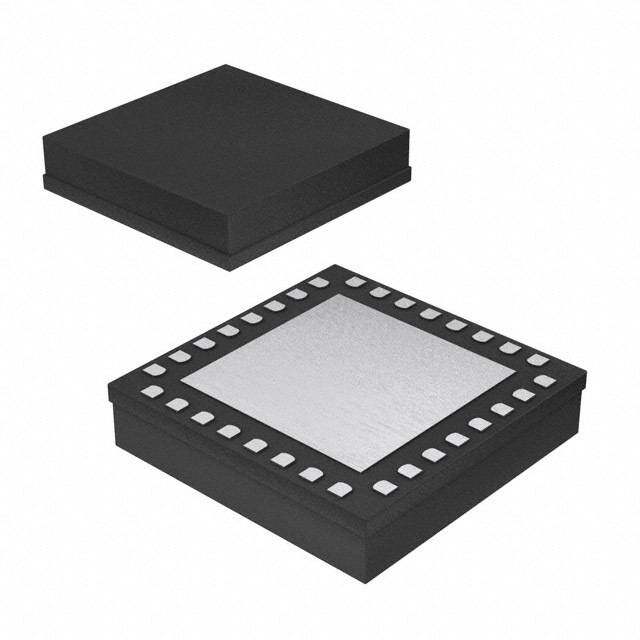
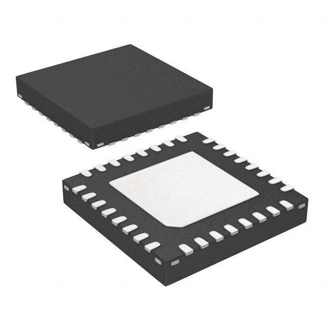
| 产品图片 |
|
| rohs | 符合RoHS无铅 / 符合限制有害物质指令(RoHS)规范要求 |
| 产品系列 | RF集成电路,射频混合器,Maxim Integrated MAX2055EUP+D- |
| 数据手册 | |
| 产品型号 | MAX2055EUP+D |
| RF类型 | 手机,ATE,PHS/PAS |
| 产品培训模块 | http://www.digikey.cn/PTM/IndividualPTM.page?site=cn&lang=zhs&ptm=25703http://www.digikey.cn/PTM/IndividualPTM.page?site=cn&lang=zhs&ptm=25705 |
| 产品种类 | 射频混合器 |
| 供应商器件封装 | 20-TSSOP-EP |
| 其它名称 | MAX2055EUPD |
| 功能 | ADC 驱动器/放大器 |
| 包装 | 管件 |
| 商标 | Maxim Integrated |
| 封装 | Tube |
| 封装/外壳 | 20-TSSOP(0.173",4.40mm 宽)裸焊盘 |
| 工厂包装数量 | 74 |
| 应用说明 | 点击此处下载产品Datasheet点击此处下载产品Datasheet点击此处下载产品Datasheet点击此处下载产品Datasheet |
| 标准包装 | 1 |
| 系列 | MAX2055 |
| 辅助属性 | 40dBm 输出 IP3 |
| 零件号别名 | MAX2055 |
| 频率 | 30MHz ~ 300MHz |


- 商务部:美国ITC正式对集成电路等产品启动337调查
- 曝三星4nm工艺存在良率问题 高通将骁龙8 Gen1或转产台积电
- 太阳诱电将投资9.5亿元在常州建新厂生产MLCC 预计2023年完工
- 英特尔发布欧洲新工厂建设计划 深化IDM 2.0 战略
- 台积电先进制程称霸业界 有大客户加持明年业绩稳了
- 达到5530亿美元!SIA预计今年全球半导体销售额将创下新高
- 英特尔拟将自动驾驶子公司Mobileye上市 估值或超500亿美元
- 三星加码芯片和SET,合并消费电子和移动部门,撤换高东真等 CEO
- 三星电子宣布重大人事变动 还合并消费电子和移动部门
- 海关总署:前11个月进口集成电路产品价值2.52万亿元 增长14.8%


PDF Datasheet 数据手册内容提取
19-2799; Rev 0; 4/03 EVAALVUAAILTAIOBNL EKIT Digitally Controlled, Variable-Gain, Differential ADC Driver/Amplifier General Description Features M The MAX2055 high-performance, digitally controlled, ♦ 30MHz to 300MHz Frequency Range A variable-gain, differential analog-to-digital converter (ADC) driver/amplifier (DVGA) is designed for use from ♦ Single-Ended-to-Differential Conversion X 30MHz to 300MHz in base station receivers. ♦ -3dB to +20dB Variable Gain 2 The device integrates a digitally controlled attenuator ♦ 40dBm Output IP3 (at All Gain States and 70MHz) 0 and a high-linearity single-ended-to-differential output 5 amplifier, which can either eliminate an external trans- ♦ 2nd Harmonic -76dBc 5 former, or can improve the even-order distortion perfor- ♦ 3rd Harmonic -69dBc mance of a transformer-coupled circuit, thus relaxing the requirements of the anti-alias filter preceding an ♦ Noise Figure: 5.8dB at Maximum Gain ADC. Targeted for ADC driver applications to adjust ♦ Digitally Controlled Gain with 1dB Resolution and gain either dynamically or as a one-time channel gain ±0.2dB Accuracy setting, the MAX2055 is ideal for applications requiring high performance. The attenuator provides 23dB of ♦ Adjustable Bias Current attenuation range with ±0.2dB accuracy. The MAX2055 is available in a thermally enhanced 20- pin TSSOP-EP package and operates over the -40°C to Ordering Information +85°C temperature range. Applications PART TEMP RANGE PIN-PACKAGE MAX2055EUP-T -40°C to +85°C 20 TSSOP-EP* Cellular Base Stations *EP = Exposed paddle. PHS/PAS Infrastructure Receiver Gain Control Broadband Systems Automatic Test Equipment Pin Configuration/ Terrestrial Links Functional Diagram High-Performance ADC Drivers TOP VIEW VCC 1 20 GND RF_IN 2 19 ATTNOUT GND 3 18 GND MAX2055 B4 4 17 ISET B3 5 16 CC ATTENUATION B2 6 LOGIC 15 AMPIN CONTROL B1 7 14 LE B0 8 13 CBP VCC 9 12 IBIAS RF_OUT- 10 11 RF_OUT+ TSSOP ________________________________________________________________Maxim Integrated Products 1 For pricing, delivery, and ordering information,please contact Maxim/Dallas Direct!at 1-888-629-4642, or visit Maxim’s website at www.maxim-ic.com.
Digitally Controlled, Variable-Gain, Differential ADC Driver/Amplifier 5 ABSOLUTE MAXIMUM RATINGS 5 All Pins to GND......................................-0.3V to +(VCC+ 0.25V) Operating Temperature Range...........................-40°C to +85°C 0 Input Signal (RF_IN)............................…………………….20dBm Junction Temperature......................................................+150°C 2 Output Power (RF_OUT)...................................................24dBm Storage Temperature Range.............................-65°C to +165°C Continuous Power Dissipation (TA= +70°C) Lead Temperature (soldering, 10s).................................+300°C X 20-Pin TSSOP (derate 21.7mW/°C above +70°C)...........2.1W A Stresses beyond those listed under “Absolute Maximum Ratings” may cause permanent damage to the device. These are stress ratings only, and functional M operation of the device at these or any other conditions beyond those indicated in the operational sections of the specifications is not implied. Exposure to absolute maximum rating conditions for extended periods may affect device reliability. DC ELECTRICAL CHARACTERISTICS (Circuit of Figure 1; VCC = +4.75V to +5.25V, GND = 0V. No input signals applied, and input and output ports are terminated with 50Ω. R1 = 1.13kΩ, TA= -40°C to +85°C. Typical values are at VCC= +5V and TA= +25°C, unless otherwise noted.) (Notes 1, 2) PARAMETER SYMBOL CONDITIONS MIN TYP MAX UNITS SUPPLY Supply Voltage VCC 4.75 5.0 5.25 V Supply Current ICC 240 290 mA ISET Current ISET 1.1 mA CONTROL INPUTS Control Bits Parallel 5 Bits Input Logic High 2 V Input Logic Low 0.6 V Input Leakage Current -1.2 +1.2 µA AC ELECTRICAL CHARACTERISTICS (Circuit of Figure 1; VCC = +4.75V to +5.25V, GND = 0V, max gain (B0 = B1 = B2 = B3 = B4 = 0), R1 = 1.13kΩ, POUT = 5dBm, fIN= 70MHz, 50Ωsystem impedance. Typical values are at VCC= +5V and TA= +25°C, unless otherwise noted.) (Notes 1, 2) PARAMETER SYMBOL CONDITIONS MIN TYP MAX UNITS Frequency Range fR 30 300 MHz Gain G 19.9 dB Amplitude Unbalance (Note 3) 0.06 dB Phase Unbalance (Note 3) 0.7 De g re es Minimum Reverse Isolation 29 dB Noise Figure NF 5.8 dB Output 1dB Compression Point P1dB 25.7 dBm f1 + f2, f1 = 70MHz, f2 = 71MHz, 5dBm/tone 2nd-Order Output Intercept Point OIP2 75 dBm at RF_OUT 3rd-Order Output Intercept Point OIP3 All gain conditions, 5dBm/tone at RF_OUT 40 dBm 2nd Harmonic 2fIN -76 dBc 3rd Harmonic 3fIN -69 dBc RF Gain-Control Range 23 dB Gain-Control Resolution 1 dB Attenuation Absolute Accuracy Compared to the ideal expected attenuation ±0.2 dB +0.05/ Attenuation Relative Accuracy Between adjacent states dB -0.2 Gain Drift Over Temperature TA = -40°C to +85°C ±0.3 dB 2 _______________________________________________________________________________________
Digitally Controlled, Variable-Gain, Differential ADC Driver/Amplifier AC ELECTRICAL CHARACTERISTICS (continued) M (Circuit of Figure 1; VCC = +4.75V to +5.25V, GND = 0V, max gain (B0 = B1 = B2 = B3 = B4 = 0), R1 = 1.13kΩ, POUT = 5dBm, fIN= 70MHz, 50Ωsystem impedance. Typical values are at VCC= +5V and TA= +25°C, unless otherwise noted.) (Notes 1, 2) A PARAMETER SYMBOL CONDITIONS MIN TYP MAX UNITS X Gain Flatness Over 50MHz Peak-to-peak for all settings 0.5 dB 2 Bandwidth 0 Attenuator Switching Time 50% control to 90% RF 40 ns 5 Input Return Loss fR = 30MHz to 300MHz, all gain conditions 15 dB 5 fR = 30MHz to 250MHz, all gain conditions 15 Output Return Loss dB fR = 250MHz to 300MHz, all gain conditions 12 Note 1: Guaranteed by design and characterization. Note 2: All limits reflect losses of external components. Output measurements are taken at RF_OUT using the application circuit shown in Figure 1. Note 3: The amplitude and phase unbalance are tested with 50Ωresistors connected from OUT+/OUT- to GND. Typical Operating Characteristics (Circuit of Figure 1, VCC= 5.0V, R1= 1.13kΩ, max gain (B0 = B1 = B2 = B3 = B4 = 0), POUT= 5dBm, TA= +25°C, unless other- wise noted.) INPUT RETURN LOSS vs. RF FREQUENCY OUTPUT RETURN LOSS vs. RF FREQUENCY SUPPLY CURRENT vs. TEMPERATURE (ALL STATES) (ALL STATES) SUPPLY CURRENT (mA) 222223456700000 VCC = 5.0VVCC = 5.2V5CVC = 4.75V MAX2055 toc01 INPUT RETURN LOSS (dB) 322110505050 MAX2055 toc02 OUTPUT RETURN LOSS (dB) 322110505050 MAX2055 toc03 220 35 35 210 40 40 -40 -15 10 35 60 85 30 60 90 120 150 180 210 240 270 300 30 60 90 120 150 180 210 240 270 300 TEMPERATURE (°C) FREQUENCY (MHz) FREQUENCY (MHz) GAIN vs. RF FREQUENCY (ALL STATES) GAIN vs. RF FREQUENCY GAIN vs. RF FREQUENCY 25 24 24 20 MAX2055 toc04 22 TA = -40°C MAX2055 toc05 22 VCC = 4.75V MAX2055 toc06 15 20 20 B) 10 B) 18 B) 18 N (d N (d TA = +25°C N (d VCC = 5.25V GAI 5 GAI 16 TA = +85°C GAI 16 VCC = 5.0V 0 14 14 -5 12 12 -10 10 10 30 60 90 120 150 180 210 240 270 300 30 60 90 120 150 180 210 240 270 300 30 60 90 120 150 180 210 240 270 300 FREQUENCY (MHz) FREQUENCY (MHz) FREQUENCY (MHz) _______________________________________________________________________________________ 3
Digitally Controlled, Variable-Gain, Differential ADC Driver/Amplifier 5 Typical Operating Characteristics (continued) 5 (Circuit of Figure 1, VCC= 5.0V, R1= 1.13kΩ, max gain (B0 = B1 = B2 = B3 = B4 = 0), POUT= 5dBm, TA= +25°C, unless other- 0 wise noted.) 2 ATTENUATION ABSOLUTE ACCURACY ATTENUATION RELATIVE ACCURACY X (ALL STATES) (ALL STATES) REVERSE ISOLATION vs. RF FREQUENCY MA ABSOLUTE ACCURACY (dB) --0000001.......42024680 MAX2055 toc07 RELATIVE ACCURACY (dB) --0000001.......42024680 MAX2055 toc08 REVERSE ISOLATION (dB) 23348260 MAX2055 toc09 -0.6 -0.6 24 -0.8 -0.8 -1.0 -1.0 20 30 60 90 120 150 180 210 240 270 300 30 60 90 120 150 180 210 240 270 300 30 60 90 120 150 180 210 240 270 300 FREQUENCY (MHz) FREQUENCY (MHz) FREQUENCY (MHz) NOISE FIGURE vs. FREQUENCY OUTPUT P-1dB vs. FREQUENCY OUTPUT P-1dB vs. FREQUENCY 8.0 27 27 7.5 MAX2055 toc10 26 TA = +85°C MAX2055 toc11 26 VCC = +5.25V MAX2055 toc12 7.0 NOISE FIGURE (dB) 566...505 TA = +85T°AC = -40°C TA = +25°C UTPUT P-1dB (dBm) 222345 TA = -40°C TA = +25°C UTPUT P-1dB (dBm) 222345 VCC = +5V VCC = +4.75V O O 5.0 22 22 4.5 4.0 21 21 30 60 90 120 150 180 210 240 270 300 30 60 90 120 150 180 210 240 270 300 30 60 90 120 150 180 210 240 270 300 FREQUENCY (MHz) FREQUENCY (MHz) FREQUENCY (MHz) OUTPUT IP3 vs. FREQUENCY OUTPUT IP3 vs. FREQUENCY INPUT IP3 vs. ATTENUATION STATE 44 44 55 42 MAX2055 toc13 42 VCC = +5.25V MAX2055 toc14 50 PAfINRT F =O1 U7=0T PMPRUHFT2z ,= Δ 5f d=B 1mMHz, MAX2055 toc15 45 40 40 OIP3 (dBm) 3368 TA = +85°C TA = +25°C TA = -40°C OIP3 (dBm) 3368 VCC = +5V VCC = +4.75V IIP3 (dBm) 334050 34 34 25 32 PRF1 = PRF2 = 5dBm 32 PRF1 = PRF2 = 5dBm 20 AT OUTPUT, Δf = 1MHz AT OUTPUT, Δf = 1MHz 30 30 15 30 60 90 120 150 180 210 240 270 300 30 60 90 120 150 180 210 240 270 300 0 4 8 12 16 20 24 FREQUENCY (MHz) FREQUENCY (MHz) ATTENUATION STATE 4 _______________________________________________________________________________________
Digitally Controlled, Variable-Gain, Differential ADC Driver/Amplifier Typical Operating Characteristics (continued) M (Circuit of Figure 1, VCC= 5.0V, R1= 1.13kΩ, max gain (B0 = B1 = B2 = B3 = B4 = 0), POUT= 5dBm, TA= +25°C, unless other- A wise noted.) X 3RD HARMONIC vs. FREQUENCY 3RD HARMONIC vs. FREQUENCY 2ND HARMONIC vs. FREQUENCY 2 -55 -55 -60 -60 TA = -40°C MAX2055 toc16 -60 MAX2055 toc17 -65 TA = -40°C TA = +85°C MAX2055 toc18 05 VCC = +5.25V 5 Bc) -65 Bc) -65 Bc) -70 d d d C ( C ( C ( MONI -70 TA = +25°C MONI -70 VCC = +5V MONI -75 HAR -75 TA = +85°C HAR -75 VCC = +4.75V HAR -80 TA = +25°C -80 -80 -85 -85 -85 -90 30 60 90 120 150 180 210 240 270 300 30 60 90 120 150 180 210 240 270 300 30 60 90 120 150 180 210 240 270 300 FREQUENCY (MHz) FREQUENCY (MHz) FREQUENCY (MHz) 2ND HARMONIC vs. FREQUENCY OUTPUT IP2 vs. FREQUENCY (f1 + f2) OUTPUT IP2 vs. FREQUENCY (f1 + f2) -60 85 85 -65 MAX2055 toc19 80 TA = +25°C MAX2055 toc20 80 VCC =V +C5C. 0= +4.75V MAX2055 toc21 VCC = +5.25V 75 75 ONIC (dBc) --7750 2 (dBm) 70 2 (dBm) 70 ARM OIP 65 OIP 65 VCC = +5.25V H -80 VCC = +5V VCC = +4.75V 60 TA = -40°C TA = +85°C 60 -85 55 PRF1 = PRF2 = 5dBm 55 PRF1 = PRF2 = 5dBm AT OUTPUT, Δf = 1MHz AT OUTPUT, Δf = 1MHz -90 50 50 30 60 90 120 150 180 210 240 270 300 30 60 90 120 150 180 210 240 270 300 30 60 90 120 150 180 210 240 270 300 FREQUENCY (MHz) FREQUENCY (MHz) FREQUENCY (MHz) OUTPUT-PORT AMPLITUDE UNBALANCE OUTPUT-PORT PHASE UNBALANCE vs. FREQUENCY vs. FREQUENCY E UNBALANCE (dB) 000...122505 MAX2055 toc22 ALANCE (DEGREES) 1223....5050 MAX2055 toc23 UD 0.10 NB MPLIT ASE U 1.0 A 0.05 PH 0.5 0 0 30 60 90 120 150 180 210 240 270 300 30 60 90 120 150 180 210 240 270 300 FREQUENCY (MHz) FREQUENCY (MHz) _______________________________________________________________________________________ 5
Digitally Controlled, Variable-Gain, Differential ADC Driver/Amplifier 5 Typical Operating Characteristics (continued) 5 (Circuit of Figure 2, VCC= 5.0V, R1= 909Ω, max gain, (B0 = B1 = B2 = B3 = B4 = 0), POUT= 5dBm, TA= +25°C, unless otherwise 0 noted.) 2 INPUT RETURN LOSS vs. RF FREQUENCY OUTPUT RETURN LOSS vs. FREQUENCY X SUPPLY CURRENT vs. TEMPERATURE (ALL STATES) (ALL STATES) MA SUPPLY CURRENT (mA) 222223456700000 VCC = 5.0V VCC =V 5C.2C5 =V 4.75V MAX2055 toc24 INPUT RETURN LOSS (dB) 432100000 MAX2055 toc25 OUTPUT RETURN LOSS (dB) 432100000 MAX2055 toc26 220 50 50 210 60 60 -40 -15 10 35 60 85 30 60 90 120 150 180 210 240 270 300 30 60 90 120 150 180 210 240 270 300 TEMPERATURE (°C) FREQUENCY (MHz) FREQUENCY (MHz) GAIN vs. RF FREQUENCY (ALL STATES) GAIN vs. RF FREQUENCY GAIN vs. RF FREQUENCY 25 24 24 20 MAX2055 toc27 22 TA = -40°C MAX2055 toc28 22 VCC = 4.75V MAX2055 toc29 15 20 20 B) 10 B) 18 B) 18 d d d GAIN ( 5 GAIN ( 16 TA = +25°C GAIN ( 16 VCC = 5.25V VCC = 5.0V TA = +85°C 0 14 14 -5 12 12 -10 10 10 30 60 90 120 150 180 210 240 270 300 30 60 90 120 150 180 210 240 270 300 30 60 90 120 150 180 210 240 270 300 FREQUENCY (MHz) FREQUENCY (MHz) FREQUENCY (MHz) ATTENUATION ABSOLUTE ACCURACY ATTENUATION RELATIVE ACCURACY (ALL STATES) (ALL STATES) REVERSE ISOLATION vs. RF FREQUENCY ABSOLUTE ACCURACY (dB) --0000001.......42024680 MAX2055 toc30 RELATIVE ACCURACY (dB) --0000001.......42024680 MAX2055 toc31 REVERSE ISOLATION (dB) 23348260 MAX2055 toc32 -0.6 -0.6 24 -0.8 -0.8 -1.0 -1.0 20 30 60 90 120 150 180 210 240 270 300 30 60 90 120 150 180 210 240 270 300 30 60 90 120 150 180 210 240 270 300 FREQUENCY (MHz) FREQUENCY (MHz) FREQUENCY (MHz) 6 _______________________________________________________________________________________
Digitally Controlled, Variable-Gain, Differential ADC Driver/Amplifier Typical Operating Characteristics (continued) M (Circuit of Figure 2, VCC= 5.0V, R1= 909Ω, max gain, (B0 = B1 = B2 = B3 = B4 = 0), POUT= 5dBm, TA= +25°C, unless otherwise A noted.) X NOISE FIGURE vs. FREQUENCY OUTPUT P-1dB vs. FREQUENCY OUTPUT P-1dB vs. FREQUENCY 2 8.0 27 27 7.5 TA = +85°C MAX2055 toc33 26 TA = +85°C MAX2055 toc34 26 VCC = +5.25V MAX2055 toc35 05 7.0 5 OISE FIGURE (dB) 566...505 TPUT P-1dB (dBm) 2245 TA = -40°C TA = +25°C TPUT P-1dB (dBm) 2245 VCC = +4.75V VCC = +5V N TA = +25°C OU 23 OU 23 5.0 22 22 4.5 TA = -40°C 4.0 21 21 30 60 90 120 150 180 210 240 270 300 30 60 90 120 150 180 210 240 270 300 30 60 90 120 150 180 210 240 270 300 FREQUENCY (MHz) FREQUENCY (MHz) FREQUENCY (MHz) OUTPUT IP3 vs. FREQUENCY OUTPUT IP3 vs. FREQUENCY INPUT IP3 vs. ATTENUATION STATE 44 44 55 42 TA = +25°C MAX2055 toc36 42 VCC = +5.25V MAX2055 toc37 50 PAfINRT F =O1 U7=0T PMPRUHFT2z ,= Δ 5f d=B 1mMHz, MAX2055 toc38 45 40 40 VCC = +4.75V OIP3 (dBm) 3368 TA = +85°C OIP3 (dBm) 3368 VCC = +5V IIP3 (dBm) 334050 34 TA = -40°C 34 25 32 PRF1 = PRF2 = 5dBm 32 PRF1 = PRF2 = 5dBm 20 AT OUTPUT, Δf = 1MHz AT OUTPUT, Δf = 1MHz 30 30 15 30 60 90 120 150 180 210 240 270 300 30 60 90 120 150 180 210 240 270 300 0 4 8 12 16 20 24 FREQUENCY (MHz) FREQUENCY (MHz) ATTENUATION STATE 3RD HARMONIC vs. FREQUENCY 3RD HARMONIC vs. FREQUENCY 2ND HARMONIC vs. FREQUENCY -55 -55 -50 -60 MAX2055 toc39 -60 MAX2055 toc40 -55 MAX2055 toc41 -60 TA = +25°C TA = -40°C dBc) -65 dBc) -65 dBc) -65 NIC ( -70 TA = -40°C NIC ( -70 VCC = +5.25V NIC ( -70 O O O RM RM VCC = +5V RM A A A -75 H -75 H -75 H -80 -80 TA = +85°C TA = +25°C -80 -85 TA = +85°C VCC = +4.75V -85 -85 -90 30 60 90 120 150 180 210 240 270 300 30 60 90 120 150 180 210 240 270 300 30 60 90 120 150 180 210 240 270 300 FREQUENCY (MHz) FREQUENCY (MHz) FREQUENCY (MHz) _______________________________________________________________________________________ 7
Digitally Controlled, Variable-Gain, Differential ADC Driver/Amplifier 5 Typical Operating Characteristics (continued) 5 (Circuit of Figure 2, VCC= 5.0V, R1= 909Ω, max gain, (B0 = B1 = B2 = B3 = B4 = 0), POUT= 5dBm, TA= +25°C, unless otherwise 0 noted.) 2 X 2ND HARMONIC vs. FREQUENCY OUTPUT IP2 vs. FREQUENCY (f1 + f2) OUTPUT IP2 vs. FREQUENCY (f1 + f2) -50 85 80 MA --6505 MAX2055 toc42 80 TA = +85°C MAX2055 toc43 75 VCC = +5.0V MAX2055 toc44 ONIC (dBc) --7605 VCC = +5.25V 2 (dBm) 7705 2 (dBm) 6750 VCC = +4.75V HARM -75 VCC = +5V VCC = +4.75V OIP 6605 TA = +25°C OIP 60 VCC = +5.25V -80 TA = -40°C -85 55 PRF1 = PRF2 = 5dBm 55 PRF1 = PRF2 = 5dBm AT OUTPUT, Δf = 1MHz AT OUTPUT, Δf = 1MHz -90 50 50 30 60 90 120 150 180 210 240 270 300 30 60 90 120 150 180 210 240 270 300 30 60 90 120 150 180 210 240 270 300 FREQUENCY (MHz) FREQUENCY (MHz) FREQUENCY (MHz) OUTPUT-PORT AMPLITUDE UNBALANCE OUTPUT-PORT PHASE UNBALANCE vs. FREQUENCY vs. FREQUENCY 0.25 3.0 PLITUDE UNBALANCE (dB) 000...112050 MAX2055 toc45 SE UNBALANCE (DEGREES) 1122....0505 MAX2055 toc46 M A A 0.05 PH 0.5 0 0 30 60 90 120 150 180 210 240 270 300 30 60 90 120 150 180 210 240 270 300 FREQUENCY (MHz) FREQUENCY (MHz) 8 _______________________________________________________________________________________
Digitally Controlled, Variable-Gain, Differential ADC Driver/Amplifier Pin Description M A PIN NAME FUNCTION X Power Supply. Bypass to GND with capacitors as close to the pin as possible as shown in the typical 1, 9 VCC 2 application circuits (Figures 1 and 2). 0 Signal Input. Internally matched to 50Ω over the operating frequency. See the typical application 2 RF_IN 5 circuit for recommended component values. 5 Ground. Use low-inductance layout techniques on the PC board. Solder the exposed paddle to the 3, 18, 20, EP GND board ground plane. 4–8 B4–B0 Attenuation Control Bits. Digital input for attenuation control. See Table 3 for attenuation setting. Inverted Differential Signal Output. Requires an external pullup choke inductor (120mA typical 10 RF_OUT- current) to VCC along with a DC-blocking capacitor; see Figures 1 and 2. Noninverted Differential Signal Output. Requires an external pullup choke inductor (120mA typical 11 RF_OUT+ current) to VCC along with a DC-blocking capacitor; see Figures 1 and 2. 12 IBIAS Amplifier Bias Input. See Figures 1 and 2 for detailed connection. 13 CBP Bypass Capacitor. See Figures 1 and 2 for detailed connection. Amplifier DC Ground. Requires choke inductor that can handle supply current. DC resistance of 14 LE inductor should be less than 0.2Ω. 15 AMPIN Amplifier Input. Requires DC-coupling to allow biasing. 16 CC Compensation Capacitor. Requires connection to AMPIN (pin 15) for stability. 17 ISET Connect R1 from ISET to GND (see Table 1 or Table 2 for values). 19 ATTNOUT Attenuator Output. Requires external DC-blocking capacitor. Table 1. Suggested Components of Table 2. Suggested Components of Circuit of Figure 1 Circuit of Figure 2 COMPONENT VALUE SIZE COMPONENT VALUE SIZE C1, C3–C6, C8, C9, C10, C12 1nF 0603 C1, C3, C4, C5, C7–C10, C12 1nF 0603 C2, C11 100pF 0603 C2, C11 100pF 0603 L1, L3 330nH 0603 L1, L2, L3 330nH 0603 L2 100nH 0603 L4, L5 680nH 1008 L4, L5 680nH 1008 R1 909Ω 0603 R1 1.13kΩ 0603 R7 10Ω 0603 R7 10Ω 0603 T2 1:1 — T1, T2 1:1 — _______________________________________________________________________________________ 9
Digitally Controlled, Variable-Gain, Differential ADC Driver/Amplifier 5 5 VCC 0 2 C3 C2 X C4 C6 A 1 20 VCC GND M RF_IN 2 RF_IN ATTNOUT 19 C1 3 GND GND 18 T1 R1 4 B4 ISET 17 C5 5 B3 16 CC 1 ATTENUATION CONTROL 6 B2 LOGIC AMPIN 15 INPUTS 7 B1 CONTROL 14 L2 LE 8 B0 CBP 13 L1 R7 VCC 9 VCC MAX2055 IBIAS 12 11 L3 C12 C11 10 RF_OUT- RF_OUT+ L5 VCC L4 C10 C8 C9 1 T2 RF_OUT Figure 1. Typical Application Circuit Detailed Description feedback to achieve high gain and linearity over a wide bandwidth. The MAX2055 is a high-dynamic-range, digitally con- trolled, variable-gain differential ADC driver/amplifier Applications Information (DVGA) for use in applications from 30MHz to 300MHz. The amplifier is designed for 50Ω single-ended input Digitally Controlled Attenuator and 50Ωdifferential output systems. The digital attenuator is controlled through five logic lines: B0, B1, B2, B3, and B4. Table 3 lists the attenua- The MAX2055 integrates a digital attenuator with a tion settings. The input and output of this attenuator 23dB selectable attenuation range and a high-linearity, require external DC blocking capacitors. The attenua- single-ended-to-differential output amplifier. The attenu- tor’s insertion loss is approximately 2dB, when the con- ator is digitally controlled through five logic lines: trol bits are set to 0dB (B0 = B1 = B2 = B3 = B4 = 0). B0–B4. The on-chip attenuator provides up to 23dB of attenuation with ±0.2dB accuracy. The single-ended Single-Ended-to-Differential Amplifier input to differential output amplifier utilizes negative The MAX2055 integrates a single-ended-to-differential amplifier with a nominal gain of 22dB in a negative 10 ______________________________________________________________________________________
Digitally Controlled, Variable-Gain, Differential ADC Driver/Amplifier M VCC A X C3 C2 2 0 1 VCC GND 20 5 RF_IN 2 RF_IN ATTNOUT 19 5 C1 3 GND GND 18 4 B4 ISET 17 R1 C4 C5 5 B3 CC 16 ATTENUATION CONTROL 6 B2 LOGIC AMPIN 15 INPUTS 7 B1 CONTROL LE 14 L2 8 B0 CBP 13 L1 R7 VCC 9 VCC MAX2055 IBIAS 12 C7 C12 C11 11 L3 10 RF_OUT- RF_OUT+ L5 VCC L4 C10 C8 C9 1 T2 RF_OUT Figure 2. Low-Cost Application Circuit feedback topology. This amplifier is optimized for a fre- Choke Inductor quency range of operation from 30MHz to 300MHz with The single-ended amplifier input and differential output a high-output third-order intercept point (OIP3). The ports require external choke inductors. At the input, bias current is chosen to optimize the IP3 of the amplifi- connect a 330nH bias inductor from AMPIN (pin 15) to er. When R1 is 1.13kΩ (909Ω if using the circuit of IBIAS (pin 12). Connect 680nH choke inductors from Figure 2), the current consumption is 240mA while RF_OUT+ (pin 11) and RF_OUT- (pin 10) to VCC. These exhibiting a 40dBm typical output IP3 at 70MHz. The connections provide bias current to the amplifier. common-mode inductor, L2, provides a high common- Layout Considerations mode rejection with excellent amplitude and phase bal- ance at the output. L2 must handle the supply current A properly designed PC board is an essential part of and have DC resistance less than 0.2Ω. any RF/microwave circuit. Keep RF signal lines as short as possible to reduce losses, radiation, and induc- tance. For best performance, route the ground-pin traces directly to the exposed pad underneath the ______________________________________________________________________________________ 11
Digitally Controlled, Variable-Gain, Differential ADC Driver/Amplifier 5 package. This pad should be connected to the ground Table 3. Attenuation Setting vs. Gain- 5 plane of the board by using multiple vias under the Control Bits device to provide the best RF/thermal conduction path. 0 2 Solder the exposed pad on the bottom of the device ATTENUATION B4 B3* B2 B1 B0 package to a PC board exposed pad. X 0 0 0 0 0 0 The MAX2055 Evaluation Kit can be used as a refer- A 1 0 0 0 0 1 ence for board layout. Gerber files are available upon 2 0 0 0 1 0 M request at www.maxim-ic.com. 3 0 0 0 1 1 Power-Supply Bypassing 4 0 0 1 0 0 Proper voltage-supply bypassing is essential for high- 5 0 0 1 0 1 frequency circuit stability. Bypass each VCC pin with a 1000pF and 100pF capacitor. Connect the 100pF 6 0 0 1 1 0 capacitor as close to the device as possible. Resistor 7 0 0 1 1 1 R7 helps reduce switching transients. If switching tran- 8 0 1 0 0 0 sients are not a concern, R7 is not required. Therefore, 9 0 1 0 0 1 connect pin 9 directly to VCC. 10 0 1 0 1 0 Exposed Paddle RF Thermal 11 0 1 0 1 1 Considerations 12 0 1 1 0 0 The EP of the MAX2055’s 20-pin TSSOP-EP package provides a low thermal-resistance path to the die. It is 13 0 1 1 0 1 important that the PC board on which the IC is mounted 14 0 1 1 1 0 be designed to conduct heat from this contact. In addi- 15 0 1 1 1 1 tion, the EP provides a low-inductance RF ground path 16 1 X 0 0 0 for the device. 17 1 X 0 0 1 It is recommended that the EP be soldered to a ground 18 1 X 0 1 0 plane on the PC board, either directly or through an array of plated via holes. 19 1 X 0 1 1 Soldering the pad to ground is also critical for efficient 20 1 X 1 0 0 heat transfer. Use a solid ground plane wherever 21 1 X 1 0 1 possible. 22 1 X 1 1 0 23 1 X 1 1 1 Chip Information *Enabling B4 disables B3 and the minimum attenuation is 16dB. TRANSISTOR COUNT: 325 PROCESS: BiCMOS 12 ______________________________________________________________________________________
Digitally Controlled, Variable-Gain, Differential ADC Driver/Amplifier Package Information M (The package drawing(s) in this data sheet may not reflect the most current specifications. For the latest package outline information, A go to www.maxim-ic.com/packages.) X S 2 P E m. 0 m 40 5 4. P O 5 S S T PACKAGE OUTLINE, TSSOP 4.40mm BODY 1 21-0066 I 1 Maxim cannot assume responsibility for use of any circuitry other than circuitry entirely embodied in a Maxim product. No circuit patent licenses are implied. Maxim reserves the right to change the circuitry and specifications without notice at any time. Maxim Integrated Products, 120 San Gabriel Drive, Sunnyvale, CA 94086 408-737-7600 ____________________13 © 2003 Maxim Integrated Products Printed USA is a registered trademark of Maxim Integrated Products.
Mouser Electronics Authorized Distributor Click to View Pricing, Inventory, Delivery & Lifecycle Information: M axim Integrated: MAX2055EUP+D MAX2055EUP+TD