ICGOO在线商城 > 射频/IF 和 RFID > RF 其它 IC 和模块 > AD6655ABCPZ-125
 Datasheet下载
- 型号: AD6655ABCPZ-125
- 制造商: Analog
- 库位|库存: xxxx|xxxx
- 要求:
| 数量阶梯 | 香港交货 | 国内含税 |
| +xxxx | $xxxx | ¥xxxx |
查看当月历史价格
查看今年历史价格
AD6655ABCPZ-125产品简介:
ICGOO电子元器件商城为您提供AD6655ABCPZ-125由Analog设计生产,在icgoo商城现货销售,并且可以通过原厂、代理商等渠道进行代购。 AD6655ABCPZ-125价格参考¥710.39-¥822.21。AnalogAD6655ABCPZ-125封装/规格:RF 其它 IC 和模块, RF IC IF Diversity Receiver GSM, EDGE, CDMA 0Hz ~ 450MHz Sample Rates to 125MSPS 64-LFCSP-VQ (9x9)。您可以下载AD6655ABCPZ-125参考资料、Datasheet数据手册功能说明书,资料中有AD6655ABCPZ-125 详细功能的应用电路图电压和使用方法及教程。
AD6655ABCPZ-125 是由 Analog Devices Inc.(ADI)生产的一款高性能 RF(射频)相关 IC,属于 ADI 的高速模数转换器 (ADC) 系列。其主要应用场景包括:

1. 通信系统
   - 适用于无线基站、软件定义无线电(SDR)、点对点无线电通信等场景。该器件能够处理宽带信号,支持多载波和多模式通信标准,例如 GSM、CDMA、WCDMA 和 LTE。
   - 高速采样能力使其适合于需要高动态范围和低失真的通信应用。

2. 雷达与国防
   - 在雷达系统中用于目标检测和跟踪,支持脉冲压缩和多普勒处理。
   - 可应用于电子战(EW)系统,提供宽频带信号采集能力,以满足复杂的信号环境需求。

3. 测试与测量设备
   - 用于频谱分析仪、矢量信号分析仪和其他高性能测试设备中,能够精确捕获和分析高频信号。
   - 其出色的线性度和低噪声性能确保了测量结果的准确性。

4. 航空航天与导航
   - 在卫星通信、全球定位系统(GPS)增强技术以及航空电子设备中发挥作用。
   - 支持高精度的数据采集,有助于提升导航系统的可靠性和抗干扰能力。

5. 医疗成像
   - 虽然不是直接面向医疗领域设计,但其高性能特性可用于超声波成像、核磁共振(MRI)等需要高速数据采集的应用。

总结来说,AD6655ABCPZ-125 凭借其卓越的采样率(最高可达 125 MSPS)、高分辨率(14 位)以及低功耗特性,广泛应用于需要处理复杂射频信号的各种高端技术领域。
| 参数 | 数值 |
| 产品目录 | |
| 描述 | IC IF RCVR 14BIT 125MSPS 64LFCSP模数转换器 - ADC IC 14 Bit IF Diversity Receiver |
| 产品分类 | |
| 品牌 | Analog Devices Inc |
| 产品手册 | |
| 产品图片 |
|
| rohs | 符合RoHS无铅 / 符合限制有害物质指令(RoHS)规范要求 |
| 产品系列 | 数据转换器IC,模数转换器 - ADC,Analog Devices AD6655ABCPZ-125- |
| 数据手册 | |
| 产品型号 | AD6655ABCPZ-125 |
| RF类型 | GSM,EDGE,CDMA |
| 产品种类 | 模数转换器 - ADC |
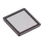
| 供应商器件封装 | 64-LFCSP-VQ(9x9) |
| 信噪比 | 74.9 dB |
| 其它名称 | AD6655ABCPZ125 |
| 分辨率 | 14 bit |
| 功能 | IF 分集接收器 |
| 包装 | 托盘 |
| 商标 | Analog Devices |
| 安装风格 | SMD/SMT |
| 封装 | Tray |
| 封装/外壳 | 64-VFQFN 裸露焊盘,CSP |
| 封装/箱体 | LFCSP EP |
| 工作电源电压 | 1.9 V |
| 工厂包装数量 | 260 |
| 接口类型 | Parallel |
| 最大工作温度 | + 85 C |
| 最小工作温度 | - 40 C |
| 标准包装 | 1 |
| 系列 | AD6655 |
| 结构 | Pipeline |
| 视频文件 | http://www.digikey.cn/classic/video.aspx?PlayerID=1364138032001&width=640&height=505&videoID=2245193150001 |
| 转换速率 | 80 MSPs |
| 辅助属性 | 采样率达 125MSPS |
| 输入类型 | Single-Ended/Differential |
| 通道数量 | 2 Channel |
| 频率 | 0Hz ~ 450MHz |


- 商务部:美国ITC正式对集成电路等产品启动337调查
- 曝三星4nm工艺存在良率问题 高通将骁龙8 Gen1或转产台积电
- 太阳诱电将投资9.5亿元在常州建新厂生产MLCC 预计2023年完工
- 英特尔发布欧洲新工厂建设计划 深化IDM 2.0 战略
- 台积电先进制程称霸业界 有大客户加持明年业绩稳了
- 达到5530亿美元!SIA预计今年全球半导体销售额将创下新高
- 英特尔拟将自动驾驶子公司Mobileye上市 估值或超500亿美元
- 三星加码芯片和SET,合并消费电子和移动部门,撤换高东真等 CEO
- 三星电子宣布重大人事变动 还合并消费电子和移动部门
- 海关总署:前11个月进口集成电路产品价值2.52万亿元 增长14.8%


PDF Datasheet 数据手册内容提取
IF Diversity Receiver Data Sheet AD6655 FEATURES APPLICATIONS SNR = 74.5 dBc (75.5 dBFS) in a 32.7 MHz BW at Communications 70 MHz at 150 MSPS Diversity radio systems SFDR = 80 dBc to 70 MHz at 150 MSPS Multimode digital receivers (3G) 1.8 V analog supply operation TD-SCDMA, WiMax, WCDMA, 1.8 V to 3.3 V CMOS output supply or 1.8 V LVDS CDMA2000, GSM, EDGE, LTE output supply I/Q demodulation systems Integer 1-to-8 input clock divider Smart antenna systems Integrated dual-channel ADC General-purpose software radios Sample rates up to 150 MSPS Broadband data applications IF sampling frequencies to 450 MHz PRODUCT HIGHLIGHTS Internal ADC voltage reference Integrated ADC sample-and-hold inputs 1. Integrated dual, 14-bit, 150 MSPS ADC. Flexible analog input range: 1 V p-p to 2 V p-p 2. Integrated wideband decimation filter and 32-bit ADC clock duty cycle stabilizer complex NCO. 95 dB channel isolation/crosstalk 3. Fast overrange detect and signal monitor with serial output. Integrated wideband digital downconverter (DDC) 4. Proprietary differential input maintains excellent SNR 32-bit complex, numerically controlled oscillator (NCO) performance for input frequencies up to 450 MHz. Decimating half-band filter and FIR filter 5. Flexible output modes, including independent CMOS, Supports real and complex output modes interleaved CMOS, IQ mode CMOS, and interleaved LVDS. Fast attack/threshold detect bits 6. SYNC input allows synchronization of multiple devices. Composite signal monitor Energy-saving power-down modes 7. 3-bit SPI port for register programming and register readback. FUNCTIONAL BLOCK DIAGRAM AVDD FD[0:3]A DVDD DRVDD FD BITS/THRESHOLD AD6655 DETECT R I SFE VIN+A LP/HP VDUF D13A VIN–A SHA ADC Q DHEBC FIFMILIARTTEIRN G+ MOS/LPUT B D0A CUT O VREF DIVIDE 1 CLK+ TO 8 SECNMSEL SERLEEFCT MSOIGNNITAOLR T3UN2N-CBIONITG fANDCCO/8 STCADYBUCITLLYIZEER GENEDRCAOTION CDDLCCKOO–AB RBIAS R Q E F VIN–B DECLIPM/AHTPING OSBUF D13B SHA ADC HB FILTER + MT VIN+B I FIR PROGRAMMING DATA CPU D0B T U O MULTI-CHIP FD BITS/THRESHOLD SIGNAL MONITOR SIGNAL MONITOR SPI SYNC DETECT DATA INTERFACE AGND SYNC FD[0:3]B SMI SMI SMI SDIO/SCLK/ CSB DRGND SDFSSCLK/ SDO/ DCS DFS N1.OPTINE SNAMES ARE FOR THE CMOS PIN CONFIGURATION ONLY; SEE FIGURE 10 FOPRD LWVNDSO PEINB NAMES. 06709-001 Figure 1. Rev. B Document Feedback Information furnished by Analog Devices is believed to be accurate and reliable. However, no responsibility is assumed by Analog Devices for its use, nor for any infringements of patents or other One Technology Way, P.O. Box 9106, Norwood, MA 02062-9106, U.S.A. rights of third parties that may result from its use. Specifications subject to change without notice. No license is granted by implication or otherwise under any patent or patent rights of Analog Devices. Tel: 781.329.4700 ©2007–2014 Analog Devices, Inc. All rights reserved. Trademarks and registered trademarks are the property of their respective owners. Technical Support www.analog.com
AD6655 Data Sheet TABLE OF CONTENTS Features .............................................................................................. 1 Decimating Half-Band Filter and FIR filter ................................ 39 Applications ....................................................................................... 1 Half-Band Filter Coefficients .................................................... 39 Product Highlights ........................................................................... 1 Half-Band Filter Features .......................................................... 39 Functional Block Diagram .............................................................. 1 Fixed-Coefficient FIR Filter ...................................................... 39 Revision History ............................................................................... 3 Synchronization .......................................................................... 40 General Description ......................................................................... 4 Combined Filter Performance .................................................. 40 Specifications ..................................................................................... 5 Final NCO ................................................................................... 40 ADC DC Specifications—AD6655-80/AD6655-105 .............. 5 ADC Overrange and Gain Control .............................................. 41 ADC DC Specifications—AD6655-125/AD6655-150 ............ 6 Fast Detect Overview ................................................................. 41 ADC AC Specifications—AD6655-80/AD6655-105 ............... 7 ADC Fast Magnitude ................................................................. 41 ADC AC Specifications—AD6655-125/AD6655-150 ............. 8 ADC Overrange (OR) ................................................................ 42 Digital Specifications—AD6655-80/AD6655-105 ................... 9 Gain Switching ............................................................................ 42 Digital Specifications—AD6655-125/AD6655-150 ............... 11 Signal Monitor ................................................................................ 44 Switching Specifications—AD6655-80/AD6655-105 ............ 13 Peak Detector Mode................................................................... 44 Switching Specifications—AD6655-125/AD6655-150 ......... 14 RMS/MS Magnitude Mode ....................................................... 44 Timing Specifications ................................................................ 15 Threshold Crossing Mode ......................................................... 45 Absolute Maximum Ratings .......................................................... 18 Additional Control Bits ............................................................. 45 Thermal Characteristics ............................................................ 18 DC Correction ............................................................................ 45 ESD Caution ................................................................................ 18 Signal Monitor SPORT Output ................................................ 46 Pin Configurations and Function Descriptions ......................... 19 Channel/Chip Synchronization .................................................... 47 Equivalent Circuits ......................................................................... 23 Serial Port Interface (SPI) .............................................................. 48 Typical Performance Characteristics ........................................... 24 Configuration Using the SPI ..................................................... 48 Theory of Operation ...................................................................... 29 Hardware Interface ..................................................................... 48 ADC Architecture ...................................................................... 29 Configuration Without the SPI ................................................ 49 Analog Input Considerations .................................................... 29 SPI Accessible Features .............................................................. 49 Voltage Reference ....................................................................... 31 Memory Map .................................................................................. 50 Clock Input Considerations ...................................................... 32 Reading the Memory Map Register Table ............................... 50 Power Dissipation and Standby Mode ..................................... 34 Memory Map Register Table ..................................................... 51 Digital Outputs ........................................................................... 35 Memory Map Register Description ......................................... 55 Digital Downconverter .................................................................. 37 Applications Information .............................................................. 59 Downconverter Modes .............................................................. 37 Design Guidelines ...................................................................... 59 Numerically Controlled Oscillator (NCO) ............................. 37 Evaluation Board ............................................................................ 61 Half-Band Decimating Filter and FIR Filter ........................... 37 Power Supplies ............................................................................ 61 f /8 Fixed-Frequency NCO ................................................... 37 Input Signals................................................................................ 61 ADC Numerically Controlled Oscillator (NCO) ................................. 38 Output Signals ............................................................................ 61 Frequency Translation ............................................................... 38 Default Operation and Jumper Selection Settings ................. 62 NCO Synchronization ............................................................... 38 Alternative Clock Configurations ............................................ 62 Phase Offset ................................................................................. 38 Alternative Analog Input Drive Configuration...................... 63 NCO Amplitude and Phase Dither .......................................... 38 Schematics ................................................................................... 64 Rev. B | Page 2 of 84
Data Sheet AD6655 Evaluation Board Layouts .......................................................... 74 Ordering Guide ........................................................................... 84 Bill of Materials ........................................................................... 82 Outline Dimensions ........................................................................ 84 REVISION HISTORY 1/14—Rev. A to Rev. B Removed CP-63-3 Package ............................................... Universal Changes to Address 0x0D, Table 29 .............................................. 52 Changes to Memory Map Description Section ........................... 55 Updated Outline Dimensions ........................................................ 84 9/09—Rev. A to Rev. 0 Added Exposed Pad Notation to Figure 9 and Table 12 ............ 19 Added Exposed Pad Notation to Figure 10 and Table 13 .......... 21 Updated Outline Dimensions ........................................................ 84 Changes to Ordering Guide ........................................................... 85 11/07—Revision 0: Initial Version Rev. B | Page 3 of 84
AD6655 Data Sheet GENERAL DESCRIPTION The AD6655 is a mixed-signal intermediate frequency (IF) receiver In addition, the programmable threshold detector allows consisting of dual 14-bit, 80 MSPS/105 MSPS/125 MSPS/150 MSPS monitoring of the incoming signal power using the four fast ADCs and a wideband digital downconverter (DDC). The AD6655 detect bits of the ADC with low latency. If the input signal level is designed to support communications applications where low exceeds the programmable threshold, the coarse upper threshold cost, small size, and versatility are desired. indicator goes high. Because this threshold indicator has low latency, the user can quickly turn down the system gain to avoid The dual ADC core features a multistage, differential pipelined an overrange condition. architecture with integrated output error correction logic. Each ADC features wide bandwidth differential sample-and-hold The second AGC-related function is the signal monitor. This analog input amplifiers supporting a variety of user-selectable block allows the user to monitor the composite magnitude of the input ranges. An integrated voltage reference eases design consid- incoming signal, which aids in setting the gain to optimize the erations. A duty cycle stabilizer is provided to compensate for dynamic range of the overall system. variations in the ADC clock duty cycle, allowing the converters After digital processing, data can be routed directly to the two to maintain excellent performance. external 14-bit output ports. These outputs can be set from 1.8 V ADC data outputs are internally connected directly to the digital to 3.3 V CMOS or as 1.8 V LVDS. The CMOS data can also be downconverter (DDC) of the receiver, simplifying layout and output in an interleaved configuration at a double data rate using reducing interconnection parasitics. The digital receiver has two only Port A. channels and provides processing flexibility. Each receive channel The AD6655 receiver digitizes a wide spectrum of IF frequencies. has four cascaded signal processing stages: a 32-bit frequency Each receiver is designed for simultaneous reception of the main translator (numerically controlled oscillator (NCO)), a half- channel and the diversity channel. This IF sampling architecture band decimating filter, a fixed FIR filter, and an f /8 fixed- ADC greatly reduces component cost and complexity compared with frequency NCO. traditional analog techniques or less integrated digital methods. In addition to the receiver DDC, the AD6655 has several Flexible power-down options allow significant power savings, functions that simplify the automatic gain control (AGC) when desired. function in the system receiver. The fast detect feature allows Programming for setup and control is accomplished using a 3-bit fast overrange detection by outputting four bits of input level SPI-compatible serial interface. information with short latency. The AD6655 is available in a 64-lead LFCSP and is specified over the industrial temperature range of −40°C to +85°C. Rev. B | Page 4 of 84
Data Sheet AD6655 SPECIFICATIONS ADC DC SPECIFICATIONS—AD6655-80/AD6655-105 AVDD = 1.8 V, DVDD = 1.8 V, DRVDD = 1.8 V, maximum sample rate, VIN = −1.0 dBFS differential input, 1.0 V internal reference, DCS enabled, unless otherwise noted. Table 1. AD6655-80 AD6655-105 Parameter Temperature Min Typ Max Min Typ Max Unit RESOLUTION Full 14 14 Bits ACCURACY No Missing Codes Full Guaranteed Guaranteed Offset Error Full ±0.2 ±0.6 ±0.2 ±0.6 % FSR Gain Error Full −3.6 −1.8 −0.1 −4.3 −2.2 −0.5 % FSR MATCHING CHARACTERISTIC Offset Error 25°C ±0.2 ±0.6 ±0.2 ±0.6 % FSR Gain Error 25°C ±0.2 ±0.75 ±0.2 ±0.75 % FSR TEMPERATURE DRIFT Offset Error Full ±15 ±15 ppm/°C Gain Error Full ±95 ±95 ppm/°C INTERNAL VOLTAGE REFERENCE Output Voltage Error (1 V Mode) Full ±5 ±18 ±5 ±18 mV Load Regulation at 1.0 mA Full 7 7 mV INPUT-REFERRED NOISE VREF = 1.0 V 25°C 0.85 0.85 LSB rms ANALOG INPUT Input Span, VREF = 1.0 V Full 2 2 V p-p Input Capacitance1 Full 8 8 pF VREF INPUT RESISTANCE Full 6 6 kΩ POWER SUPPLIES Supply Voltage AVDD, DVDD Full 1.7 1.8 1.9 1.7 1.8 1.9 V DRVDD (CMOS Mode) Full 1.7 3.3 3.6 1.7 3.3 3.6 V DRVDD (LVDS Mode) Full 1.7 1.8 1.9 1.7 1.8 1.9 V Supply Current IAVDD2, 3 Full 235 315 mA 420 575 IDVDD2, 3 Full 175 225 mA IDRVDD2 (3.3 V CMOS) Full 18 21 mA IDRVDD2 (1.8 V CMOS) Full 8 11 mA IDRVDD2 (1.8 V LVDS) Full 55 56 mA POWER CONSUMPTION DC Input Full 470 490 620 650 mW Sine Wave Input2 (DRVDD = 1.8 V) Full 755 995 mW Sine Wave Input2 (DRVDD = 3.3 V) Full 800 1040 mW Standby Power4 Full 52 68 mW Power-Down Power Full 2.5 8 2.5 8 mW 1 Input capacitance refers to the effective capacitance between one differential input pin and AGND. See Figure 11 for the equivalent analog input structure. 2 Measured with a 9.7 MHz, full-scale sine wave input, NCO enabled with a frequency of 13 MHz, FIR filter enabled and the fS/8 output mix enabled with approximately 5 pF loading on each output bit. 3 The maximum limit applies to the combination of IAVDD and IDVDD currents. 4 Standby power is measured with a dc input and with the CLK pin inactive (set to AVDD or AGND). Rev. B | Page 5 of 84
AD6655 Data Sheet ADC DC SPECIFICATIONS—AD6655-125/AD6655-150 AVDD = 1.8 V, DVDD = 1.8 V, DRVDD = 1.8 V, maximum sample rate, VIN = −1.0 dBFS differential input, 1.0 V internal reference, DCS enabled, unless otherwise noted. Table 2. AD6655-125 AD6655-150 Parameter Temperature Min Typ Max Min Typ Max Unit RESOLUTION Full 14 14 Bits ACCURACY No Missing Codes Full Guaranteed Guaranteed Offset Error Full ±0.3 ±0.6 ±0.2 ±0.6 % FSR Gain Error Full −4.7 −2.7 −0.8 −5.1 −3.2 −1.0 % FSR MATCHING CHARACTERISTIC Offset Error 25°C ±0.3 ±0.7 ±0.2 ±0.7 % FSR Gain Error 25°C ±0.1 ±0.7 ±0.2 ±0.8 % FSR TEMPERATURE DRIFT Offset Error Full ±15 ±15 ppm/°C Gain Error Full ±95 ±95 ppm/°C INTERNAL VOLTAGE REFERENCE Output Voltage Error (1 V Mode) Full ±5 ±18 ±5 ±18 mV Load Regulation at 1.0 mA Full 7 7 mV INPUT-REFERRED NOISE VREF = 1.0 V 25°C 0.85 0.85 LSB rms ANALOG INPUT Input Span, VREF = 1.0 V Full 2 2 V p-p Input Capacitance1 Full 8 8 pF VREF INPUT RESISTANCE Full 6 6 kΩ POWER SUPPLIES Supply Voltage AVDD, DVDD Full 1.7 1.8 1.9 1.7 1.8 1.9 V DRVDD (CMOS Mode) Full 1.7 1.8 3.6 1.7 1.8 3.6 V DRVDD (LVDS Mode) Full 1.7 1.8 1.9 1.7 1.8 1.9 V Supply Current I 2, 3 Full 390 440 mA AVDD 705 805 I 2, 3 Full 270 320 mA DVDD I 2 (3.3 V CMOS) Full 26 28 mA DRVDD I 2 (1.8 V CMOS) Full 13 17 mA DRVDD I 2 (1.8 V LVDS) Full 57 57 mA DRVDD POWER CONSUMPTION DC Input Full 770 810 870 920 mW Sine Wave Input2 (DRVDD = 1.8 V) Full 1215 1395 mW Sine Wave Input2 (DRVDD = 3.3 V) Full 1275 1450 mW Standby Power4 Full 77 77 mW Power-down Power Full 2.5 8 2.5 8 mW 1 Input capacitance refers to the effective capacitance between one differential input pin and AGND. See Figure 11 for the equivalent analog input structure. 2 Measured with a 9.7 MHz, full-scale sine wave input, NCO enabled with a frequency of 13 MHz, FIR filter enabled and the fS/8 output mix enabled with approximately 5 pF loading on each output bit. 3 The maximum limit applies to the combination of IAVDD and IDVDD currents. 4 Standby power is measured with a dc input, the CLK pin inactive (set to AVDD or AGND). Rev. B | Page 6 of 84
Data Sheet AD6655 ADC AC SPECIFICATIONS—AD6655-80/AD6655-105 AVDD = 1.8 V, DVDD = 1.8 V, DRVDD = 1.8 V, maximum sample rate, VIN = −1.0 dBFS differential input, 1.0 V internal reference, DCS enabled, NCO enabled, half-band filter enabled, FIR filter enabled, unless otherwise noted. Table 3. AD6655-80 AD6655-105 Parameter1 Temperature Min Typ Max Min Typ Max Unit SIGNAL-TO-NOISE-RATIO (SNR) f = 2.4 MHz 25°C 74.9 74.8 dB IN f = 70 MHz 25°C 74.8 74.7 dB IN Full 73.0 73.0 dB f = 140 MHz 25°C 74.5 74.3 dB IN fIN = 220 MHz 25°C 73.4 73.4 dB WORST SECOND OR THIRD HARMONIC fIN = 2.4 MHz 25°C −86 −86 dBc fIN = 70 MHz 25°C −85 −85 dBc Full −74 −74 dBc fIN = 140 MHz 25°C −84 −84 dBc fIN = 220 MHz 25°C −83 −83 dBc SPURIOUS-FREE DYNAMIC RANGE (SFDR) fIN = 2.4 MHz 25°C 86 86 dBc fIN = 70 MHz 25°C 85 85 dBc Full 74 74 dBc fIN = 140 MHz 25°C 84 84 dBc fIN = 220 MHz 25°C 83 83 dBc WORST OTHER HARMONIC OR SPUR2 fIN = 2.4 MHz 25°C −93 −93 dBc fIN = 70 MHz 25°C −90 −90 dBc Full −82 −82 dBc fIN = 140 MHz 25°C −89 −89 dBc fIN = 220 MHz 25°C −86 −86 dBc TWO-TONE SFDR fIN = 29.12 MHz, 32.12 MHz (−7 dBFS) 25°C 85 85 dBc fIN = 169.12 MHz, 172.12 MHz (−7 dBFS) 25°C 81 81 dBc CROSSTALK3 Full 95 95 dB ANALOG INPUT BANDWIDTH 25°C 650 650 MHz 1 See Application Note AN-835, Understanding High Speed ADC Testing and Evaluation, for a complete set of definitions. 2 See the Applications Information section for more information about the worst other specifications for the AD6655. 3 Crosstalk is measured at 100 MHz with −1 dBFS on one channel and with no input on the alternate channel. Rev. B | Page 7 of 84
AD6655 Data Sheet ADC AC SPECIFICATIONS—AD6655-125/AD6655-150 AVDD = 1.8 V, DVDD = 1.8 V, DRVDD = 1.8 V, maximum sample rate, VIN = −1.0 dBFS differential input, 1.0 V internal reference, DCS enabled, NCO enabled, half-band filter enabled, FIR filter enabled, unless otherwise noted. Table 4. AD6655-125 AD6655-150 Parameter1 Temperature Min Typ Max Min Typ Max Unit SIGNAL-TO-NOISE-RATIO (SNR) f = 2.4 MHz 25°C 74.7 74.6 dB IN f = 70 MHz 25°C 74.6 74.5 dB IN Full 73.0 72.5 dB f = 140 MHz 25°C 74.2 73.9 dB IN fIN = 220 MHz 25°C 73.3 73.0 dB WORST SECOND OR THIRD HARMONIC fIN = 2.4 MHz 25°C −86 −85 dBc fIN = 70 MHz 25°C −85 −84 dBc Full −73 −73 dBc fIN = 140 MHz 25°C −84 −83 dBc fIN = 220 MHz 25°C −83 −77 dBc SPURIOUS-FREE DYNAMIC RANGE (SFDR) fIN = 2.4 MHz 25°C 86 85 dBc fIN = 70 MHz 25°C 85 80 dBc Full 73 73 dBc fIN = 140 MHz 25°C 84 76 dBc fIN = 220 MHz 25°C 83 74 dBc WORST OTHER HARMONIC OR SPUR2 f = 2.4 MHz 25°C −92 −87 dBc IN f = 70 MHz 25°C −90 −80 dBc IN Full −82 −80 dBc f = 140 MHz 25°C −88 −76 dBc IN f = 220 MHz 25°C −84 −74 dBc IN TWO-TONE SFDR fIN = 29.12 MHz, 32.12 MHz (−7 dBFS) 25°C 85 85 dBc fIN = 169.12 MHz, 172.12 MHz (−7 dBFS) 25°C 81 81 dBc CROSSTALK3 Full 95 95 dB ANALOG INPUT BANDWIDTH 25°C 650 650 MHz 1 See Application Note AN-835, Understanding High Speed ADC Testing and Evaluation, for a complete set of definitions. 2 See the Applications Information section for more information about the worst other specifications for the AD6655. 3 Crosstalk is measured at 100 MHz with −1 dBFS on one channel and with no input on the alternate channel. Rev. B | Page 8 of 84
Data Sheet AD6655 DIGITAL SPECIFICATIONS—AD6655-80/AD6655-105 AVDD = 1.8 V, DVDD = 1.8 V, DRVDD = 1.8 V, maximum sample rate, VIN = −1.0 dBFS differential input, 1.0 V internal reference, DCS enabled, unless otherwise noted. Table 5. AD6655-80 AD6655-105 Parameter Temp Min Typ Max Min Typ Max Unit DIFFERENTIAL CLOCK INPUTS (CLK+, CLK−) Logic Compliance CMOS/LVDS/LVPECL CMOS/LVDS/LVPECL Internal Common-Mode Bias Full 1.2 1.2 V Differential Input Voltage Full 0.2 6 0.2 6 V p-p Input Voltage Range Full AVDD − 0.3 AVDD + 1.6 AVDD − 0.3 AVDD + 1.6 V Input Common-Mode Range Full 1.1 AVDD 1.1 AVDD V High Level Input Voltage Full 1.2 3.6 1.2 3.6 V Low Level Input Voltage Full 0 0.8 0 0.8 V High Level Input Current Full −10 +10 −10 +10 µA Low Level Input Current Full −10 +10 −10 +10 µA Input Capacitance Full 4 4 pF Input Resistance Full 8 10 12 8 10 12 kΩ SYNC INPUT Logic Compliance CMOS CMOS Internal Bias Full 1.2 1.2 V Input Voltage Range Full AVDD − 0.3 AVDD + 1.6 AVDD − 0.3 AVDD + 1.6 V High Level Input Voltage Full 1.2 3.6 1.2 3.6 V Low Level Input Voltage Full 0 0.8 0 0.8 V High Level Input Current Full −10 +10 −10 +10 µA Low Level Input Current Full −10 +10 −10 +10 µA Input Capacitance Full 4 4 pF Input Resistance Full 8 10 12 8 10 12 kΩ LOGIC INPUT (CSB)1 High Level Input Voltage Full 1.22 3.6 1.22 3.6 V Low Level Input Voltage Full 0 0.6 0 0.6 V High Level Input Current Full −10 +10 −10 +10 µA Low Level Input Current Full 40 132 40 132 µA Input Resistance Full 26 26 kΩ Input Capacitance Full 2 2 pF LOGIC INPUT (SCLK/DFS)2 High Level Input Voltage Full 1.22 3.6 1.22 3.6 V Low Level Input Voltage Full 0 0.6 0 0.6 V High Level Input Current Full −92 −135 −92 −135 µA Low Level Input Current Full −10 +10 −10 +10 µA Input Resistance Full 26 26 kΩ Input Capacitance Full 2 2 pF LOGIC INPUTS (SDIO/DCS, SMI SDFS)1 High Level Input Voltage Full 1.22 3.6 1.22 3.6 V Low Level Input Voltage Full 0 0.6 0 0.6 V High Level Input Current Full −10 +10 −10 +10 µA Low Level Input Current Full 38 128 38 128 µA Input Resistance Full 26 26 kΩ Input Capacitance Full 5 5 pF Rev. B | Page 9 of 84
AD6655 Data Sheet AD6655-80 AD6655-105 Parameter Temp Min Typ Max Min Typ Max Unit LOGIC INPUTS (SMI SDO/OEB, SMI SCLK/PDWN)2 High Level Input Voltage Full 1.22 3.6 1.22 3.6 V Low Level Input Voltage Full 0 0.6 0 0.6 V High Level Input Current Full −90 −134 −90 −134 µA Low Level Input Current Full −10 +10 −10 +10 µA Input Resistance Full 26 26 kΩ Input Capacitance Full 5 5 pF DIGITAL OUTPUTS CMOS Mode—DRVDD = 3.3 V High Level Output Voltage I = 50 µA Full 3.29 3.29 V OH I = 0.5 mA Full 3.25 3.25 V OH Low Level Output Voltage I = 1.6 mA Full 0.2 0.2 V OL I = 50 µA Full 0.05 0.05 V OL CMOS Mode—DRVDD = 1.8 V High Level Output Voltage I = 50 µA Full 1.79 1.79 V OH I = 0.5 mA Full 1.75 1.75 V OH Low Level Output Voltage I = 1.6 mA Full 0.2 0.2 V OL I = 50 µA Full 0.05 0.05 V OL LVDS Mode, DRVDD = 1.8 V Differential Output Voltage (VOD), Full 250 350 450 250 350 450 mV ANSI Mode Output Offset Voltage (VOS), Full 1.15 1.25 1.35 1.15 1.25 1.35 V ANSI Mode Differential Output Voltage (VOD), Full 150 200 280 150 200 280 mV Reduced Swing Mode Output Offset Voltage (VOS), Full 1.15 1.25 1.35 1.15 1.25 1.35 V Reduced Swing Mode 1 Pull up. 2 Pull down. Rev. B | Page 10 of 84
Data Sheet AD6655 DIGITAL SPECIFICATIONS—AD6655-125/AD6655-150 AVDD = 1.8 V, DVDD = 1.8 V, DRVDD = 1.8 V, maximum sample rate, VIN = −1.0 dBFS differential input, 1.0 V internal reference, DCS enabled, unless otherwise noted. Table 6. AD6655-125 AD6655-150 Parameter Temp Min Typ Max Min Typ Max Unit DIFFERENTIAL CLOCK INPUTS (CLK+, CLK−) Logic Compliance CMOS/LVDS/LVPECL CMOS/LVDS/LVPECL Internal Common-Mode Bias Full 1.2 1.2 V Differential Input Voltage Full 0.2 6 0.2 6 V p-p Input Voltage Range Full AVDD − 0.3 AVDD + 1.6 AVDD − 0.3 AVDD + 1.6 V Input Common-Mode Range Full 1.1 V AVDD 1.1 V AVDD V High Level Input Voltage Full 1.2 3.6 1.2 3.6 V Low Level Input Voltage Full 0 0.8 0 0.8 V High Level Input Current Full −10 +10 −10 +10 µA Low Level Input Current Full −10 +10 −10 +10 µA Input Capacitance Full 4 4 pF Input Resistance Full 8 10 12 8 10 12 kΩ SYNC INPUT Logic Compliance CMOS CMOS Internal Bias Full 1.2 1.2 V Input Voltage Range Full AVDD − 0.3 AVDD + 1.6 AVDD − 0.3 AVDD + 1.6 V High Level Input Voltage Full 1.2 3.6 1.2 3.6 V Low Level Input Voltage Full 0 0.8 0 0.8 V High Level Input Current Full −10 +10 −10 +10 µA Low Level Input Current Full −10 +10 −10 +10 µA Input Capacitance Full 4 4 pF Input Resistance Full 8 10 12 8 10 12 kΩ LOGIC INPUT (CSB)1 High Level Input Voltage Full 1.22 3.6 1.22 3.6 V Low Level Input Voltage Full 0 0.6 0 0.6 V High Level Input Current Full −10 +10 −10 +10 µA Low Level Input Current Full 40 132 40 132 µA Input Resistance Full 26 26 kΩ Input Capacitance Full 2 2 pF LOGIC INPUT (SCLK/DFS)2 High Level Input Voltage Full 1.22 3.6 1.22 3.6 V Low Level Input Voltage Full 0 0.6 0 0.6 V High Level Input Current Full −92 −135 −92 −135 µA Low Level Input Current Full −10 +10 −10 +10 µA Input Resistance Full 26 26 kΩ Input Capacitance Full 2 2 pF LOGIC INPUTS (SDIO/DCS, SMI SDFS)1 High Level Input Voltage Full 1.22 3.6 1.22 3.6 V Low Level Input Voltage Full 0 0.6 0 0.6 V High Level Input Current Full −10 +10 −10 +10 µA Low Level Input Current Full 38 128 38 128 µA Input Resistance Full 26 26 kΩ Input Capacitance Full 5 5 pF Rev. B | Page 11 of 84
AD6655 Data Sheet AD6655-125 AD6655-150 Parameter Temp Min Typ Max Min Typ Max Unit LOGIC INPUTS (SMI SDO/OEB, SMI SCLK/PDWN)2 High Level Input Voltage Full 1.22 3.6 1.22 3.6 V Low Level Input Voltage Full 0 0.6 0 0.6 V High Level Input Current Full −90 −134 −90 −134 µA Low Level Input Current Full −10 +10 −10 +10 µA Input Resistance Full 26 26 kΩ Input Capacitance Full 5 5 pF DIGITAL OUTPUTS CMOS Mode—DRVDD = 3.3 V High Level Output Voltage I = 50 µA Full 3.29 3.29 V OH I = 0.5 mA Full 3.25 3.25 V OH Low Level Output Voltage I = 1.6 mA Full 0.2 0.2 V OL I = 50 µA Full 0.05 0.05 V OL CMOS Mode—DRVDD = 1.8 V High Level Output Voltage I = 50 µA Full 1.79 1.79 V OH I = 0.5 mA Full 1.75 1.75 V OH Low Level Output Voltage I = 1.6 mA Full 0.2 0.2 V OL I = 50 µA Full 0.05 0.05 V OL LVDS Mode—DRVDD = 1.8 V Differential Output Voltage (VOD), Full 250 350 450 250 350 450 mV ANSI Mode Output Offset Voltage (VOS), Full 1.15 1.25 1.35 1.15 1.25 1.35 V ANSI Mode Differential Output Voltage (VOD), Full 150 200 280 150 200 280 mV Reduced Swing Mode Output Offset Voltage (VOS), Full 1.15 1.25 1.35 1.15 1.25 1.35 V Reduced Swing Mode 1 Pull up. 2 Pull down. Rev. B | Page 12 of 84
Data Sheet AD6655 SWITCHING SPECIFICATIONS—AD6655-80/AD6655-105 Table 7. AD6655-80 AD6655-105 Parameter Temp Min Typ Max Min Typ Max Unit CLOCK INPUT PARAMETERS Input Clock Rate Full 625 625 MHz Conversion Rate1 DCS Enabled Full 20 80 20 105 MSPS DCS Disabled Full 10 80 10 105 MSPS CLK Period—Divide-by-1 Mode (t ) Full 12.5 9.5 ns CLK CLK Pulse Width High (t ) CLKH Divide-by-1 Mode, DCS Enabled Full 3.75 6.25 8.75 2.85 4.75 6.65 ns Divide-by-1 Mode DCS Disabled Full 5.63 6.25 6.88 4.28 4.75 5.23 ns Divide-by-2 Mode, DCS Enabled Full 1.6 1.6 ns Divide-by-3 Through Divide-by-8 Modes, DCS Enabled Full 0.8 0.8 ns DATA OUTPUT PARAMETERS (DATA, FD) CMOS Noninterleaved Mode—DRVDD = 1.8 V Data Propagation Delay (t )2 Full 1.6 3.9 6.2 1.6 3.9 6.2 ns PD DCO Propagation Delay (t ) Full 4.0 5.4 7.3 4.0 5.4 7.3 ns DCO Setup Time (t) Full 14.0 11.0 ns S Hold Time (t ) Full 11.0 8.0 ns H CMOS Noninterleaved Mode—DRVDD = 3.3 V Data Propagation Delay (t )2 Full 1.9 4.1 6.4 1.9 4.1 6.4 ns PD DCO Propagation Delay (t ) Full 4.4 5.8 7.7 4.4 5.8 7.7 ns DCO Setup Time (t) Full 14.2 11.2 ns S Hold Time (t ) Full 10.8 7.8 ns H CMOS Interleaved and IQ Mode—DRVDD = 1.8 V Data Propagation Delay (t )2 Full 1.6 3.9 6.2 1.6 3.9 6.2 ns PD DCO Propagation Delay (t ) Full 3.4 4.8 6.7 3.4 4.8 6.7 ns DCO Setup Time (t) Full 7.15 5.65 ns S Hold Time (t ) Full 5.35 3.85 ns H CMOS Interleaved and IQ Mode—DRVDD = 3.3 V Data Propagation Delay (t )2 Full 1.9 4.1 6.4 1.9 4.1 6.4 ns PD DCO Propagation Delay (t ) Full 3.8 5.2 7.1 3.8 5.2 7.1 ns DCO Setup Time (t) Full 7.35 5.85 ns S Hold Time (t ) Full 5.15 3.65 ns H LVDS Mode—DRVDD = 1.8 V Data Propagation Delay (t )2 Full 2.5 4.8 7.0 2.5 4.8 7.0 ns PD DCO Propagation Delay (t ) Full 3.7 5.3 7.3 3.7 5.3 7.3 ns DCO Pipeline Delay (Latency) NCO, FIR, f/8 Mix Disabled Full 38 38 Cycles S Pipeline Delay (Latency) NCO Enabled, FIR and f/8 Mix Disabled Full 38 38 Cycles S (Complex Output Mode) Pipeline Delay (Latency) NCO, FIR, and f/8 Mix Enabled Full 109 109 Cycles S Aperture Delay (t ) Full 1.0 1.0 ns A Aperture Uncertainty (Jitter, t) Full 0.1 0.1 ps rms J Wake-Up Time3 Full 350 350 us OUT-OF-RANGE RECOVERY TIME Full 2 2 Cycles 1 Conversion rate is the clock rate after the divider. 2 Output propagation delay is measured from CLK 50% transition to DATA 50% transition, with a 5 pF load. 3 Wake-up time is dependent on the value of the decoupling capacitors. Rev. B | Page 13 of 84
AD6655 Data Sheet SWITCHING SPECIFICATIONS—AD6655-125/AD6655-150 Table 8. AD6655-125 AD6655-150 Parameter Temp Min Typ Max Min Typ Max Unit CLOCK INPUT PARAMETERS Input Clock Rate Full 625 625 MHz Conversion Rate1 DCS Enabled Full 20 125 20 150 MSPS DCS Disabled Full 10 125 10 150 MSPS CLK Period—Divide-by-1 Mode (t ) Full 8 6.66 ns CLK CLK Pulse Width High (t ) CLKH Divide-by-1 Mode, DCS Enabled Full 2.4 4 5.6 2.0 3.33 4.66 ns Divide-by-1 Mode, DCS Disabled Full 3.6 4 4.4 3.0 3.33 3.66 ns Divide-by-2 Mode, DCS Enabled Full 1.6 1.6 ns Divide-by-3 Through Divide-by-8 Modes, DCS Enabled Full 0.8 0.8 ns DATA OUTPUT PARAMETERS (DATA, FD) CMOS Noninterleaved Mode—DRVDD = 1.8 V Data Propagation Delay (t )2 Full 1.6 3.9 6.2 1.6 3.9 6.2 ns PD DCO Propagation Delay (t ) Full 4.0 5.4 7.3 4.0 5.4 7.3 ns DCO Setup Time (t) Full 9.5 8.16 ns S Hold Time (t ) Full 6.5 5.16 ns H CMOS Noninterleaved Mode—DRVDD = 3.3 V Data Propagation Delay (t )2 Full 1.9 4.1 6.4 1.9 4.1 6.4 ns PD DCO Propagation Delay (t ) Full 4.4 5.8 7.7 4.4 5.8 7.7 ns DCO Setup Time (t) Full 9.7 8.36 ns S Hold Time (t ) Full 6.3 4.96 ns H CMOS Interleaved and IQ Mode—DRVDD = 1.8 V Data Propagation Delay (t )2 Full 1.6 3.9 6.2 1.6 3.9 6.2 ns PD DCO Propagation Delay (t ) Full 3.4 4.8 6.7 3.4 4.8 6.7 ns DCO Setup Time (t) Full 4.9 4.23 ns S Hold Time (t ) Full 3.1 2.43 ns H CMOS Interleaved and IQ Mode—DRVDD = 3.3 V Data Propagation Delay (t )2 Full 1.9 4.1 6.4 1.9 4.1 6.4 ns PD DCO Propagation Delay (t ) Full 3.8 5.2 7.1 3.8 5.2 7.1 ns DCO Setup Time (t) Full 5.1 4.43 ns S Hold Time (t ) Full 2.9 2.23 ns H LVDS Mode—DRVDD = 1.8 V Data Propagation Delay (t )2 Full 2.5 4.8 7.0 2.5 4.8 7.0 ns PD DCO Propagation Delay (t ) Full 3.7 5.3 7.3 3.7 5.3 7.3 ns DCO Pipeline Delay (Latency) NCO, FIR, f/8 Mix Disabled Full 38 38 Cycles S Pipeline Delay (Latency) NCO Enabled; FIR and f/8 Mix Disabled Full 38 38 Cycles S (Complex Output Mode) Pipeline Delay (Latency) NCO, FIR, and f/8 Mix Enabled Full 109 109 Cycles S Aperture Delay (t ) Full 1.0 1.0 ns A Aperture Uncertainty (Jitter, t) Full 0.1 0.1 ps rms J Wake-Up Time3 Full 350 350 us OUT-OF-RANGE RECOVERY TIME Full 3 3 Cycles 1 Conversion rate is the clock rate after the divider. 2 Output propagation delay is measured from CLK 50% transition to DATA 50% transition, with a 5 pF load. 3 Wake-up time is dependent on the value of the decoupling capacitors. Rev. B | Page 14 of 84
Data Sheet AD6655 TIMING SPECIFICATIONS Table 9. Parameter Conditions Min Typ Max Unit SYNC TIMING REQUIREMENTS t SYNC to the rising edge of CLK setup time 0.24 ns SSYNC t SYNC to the rising edge of CLK hold time 0.4 ns HSYNC SPI TIMING REQUIREMENTS t Setup time between the data and the rising edge of SCLK 2 ns DS t Hold time between the data and the rising edge of SCLK 2 ns DH t Period of the SCLK 40 ns CLK t Setup time between CSB and SCLK 2 ns S t Hold time between CSB and SCLK 2 ns H t Minimum period that SCLK should be in a logic high state 10 ns HIGH t Minimum period that SCLK should be in a logic low state 10 ns LOW t Time required for the SDIO pin to switch from an input to an output 10 ns EN_SDIO relative to the SCLK falling edge t Time required for the SDIO pin to switch from an output to an input 10 ns DIS_SDIO relative to the SCLK rising edge SPORT TIMING REQUIREMENTS t Delay from rising edge of CLK+ to rising edge of SMI SCLK 3.2 4.5 6.2 ns CSSCLK t Delay from rising edge of SMI SCLK to SMI SDO −0.4 0 +0.4 ns SSLKSDO t Delay from rising edge of SMI SCLK to SMI SDFS −0.4 0 +0.4 ns SSCLKSDFS Timing Diagrams CLK+ tPD tDCO DECIMATED CHANNEL A/B CHANNEL A/B CHANNEL A/B CMOS DATA DATA BITS DATA BITS DATA BITS DECIMATED CHANNEL A/B CHANNEL A/B CHANNEL A/B CHANNEL A/B CHANNEL A/B CHANNEL A/B FD DATA FD BITS FD BITS FD BITS FD BITS FD BITS FD BITS tS DDCEOCAIM/DACTOEBD tH 06709-109 Figure 2. Decimated Noninterleaved CMOS Mode Data and Fast Detect Output Timing (Fast Detect Mode Select Bits = 000) CLK+ tPD tDCO DECIMATED CHANNEL A/B CHANNEL A/B CHANNEL A/B CMOS DATA DATA BITS DATA BITS DATA BITS DECIMATED CHANNEL A/B CHANNEL A/B CHANNEL A/B FD DATA FD BITS FD BITS FD BITS tS DDCEOCAIM/DACTOEBD tH 06709-012 Figure 3. Decimated Noninterleaved CMOS Mode Data and Fast Detect Output Timing (Fast Detect Mode Select Bits = 001 Through Fast Detect Mode Select Bits = 100) Rev. B | Page 15 of 84
AD6655 Data Sheet CLK+ tPD tDCO DECIMATED CHANNEL A: CHANNEL B: CHANNEL A: CHANNEL B: CHANNEL A: CHANNEL B: INTERLEAVED DATA DATA DATA DATA DATA DATA CMOS DATA DECIMATED CHANNEL A: CHANNEL B: CHANNEL A: CHANNEL B: CHANNEL A: CHANNEL B: INTERLEAVED FD BITS FD BITS FD BITS FD BITS FD BITS FD BITS FD DATA tS DECIMADTCEOD tH 06709-013 Figure 4. Decimated Interleaved CMOS Mode Data and Fast Detect Output Timing CLK+ tPD tDCO DECIMATED CHANNEL A/B: CHANNEL A/B: CHANNEL A/B: CHANNEL A/B: CHANNEL A/B: CHANNEL A/B: CMOS IQ Q DATA I DATA Q DATA I DATA Q DATA I DATA OUTPUT DATA CMOS FD CHANNEL A/B: CHANNEL A/B: CHANNEL A/B: CHANNEL A/B: CHANNEL A/B: CHANNEL A/B: DATA FD BITS FD BITS FD BITS FD BITS FD BITS FD BITS tS DDCEOCAIM/DACTOEBD tH 06709-014 Figure 5. Decimated IQ Mode CMOS Data and Fast Detect Output Timing CLK– CLK+ tPD LVDS CHANNEL A: CHANNEL B: CHANNEL A: CHANNEL B: CHANNEL A: DATA DATA DATA DATA DATA DATA LVDS CHANNEL A: CHANNEL B: CHANNEL A: CHANNEL B: CHANNEL A: FAST DET FD FD FD FD FD tDCO DCO– DCO+ 06709-015 Figure 6. Decimated Interleaved LVDS Mode Data and Fast Detect Output Timing CLK+ tSSYNC tHSYNC SYNC 06709-016 Figure 7. SYNC Timing Inputs Rev. B | Page 16 of 84
Data Sheet AD6655 CLK+ CLK– tCSSCLK SMI SCLK tSSCLKSDFS tSSCLKSDFS SMI SDFS SMI SDO DATA DATA 06709-017 Figure 8. Signal Monitor SPORT Output Timing Rev. B | Page 17 of 84
AD6655 Data Sheet ABSOLUTE MAXIMUM RATINGS Table 10. Parameter Rating THERMAL CHARACTERISTICS ELECTRICAL The exposed paddle must be soldered to the ground plane for AVDD, DVDD to AGND −0.3 V to +2.0 V the LFCSP package. Soldering the exposed paddle to the DRVDD to DRGND −0.3 V to +3.9 V customer board increases the reliability of the solder joints, AGND to DRGND −0.3 V to +0.3 V maximizing the thermal capability of the package. VIN+A/VIN+B, VIN-A/VIN−B to AGND −0.3 V to AVDD + 0.2 V CLK+, CLK− to AGND −0.3 V to +3.9 V Table 11. Thermal Resistance SYNC to AGND −0.3 V to +3.9 V Airflow VREF to AGND −0.3 V to AVDD + 0.2 V Package Velocity Type (m/s) θ 1, 2 θ 1, 3 θ 1, 4 Unit SENSE to AGND −0.3 V to AVDD + 0.2 V JA JC JB 64-Lead LFCSP 0 18.8 0.6 6.0 °C/W CML to AGND −0.3 V to AVDD + 0.2 V RBIAS to AGND −0.3 V to AVDD + 0.2 V 9 mm × 9 mm 1.0 16.5 °C/W (CP-64-6) CSB to AGND −0.3 V to +3.9 V 2.0 15.8 °C/W SCLK/DFS to DRGND −0.3 V to +3.9 V 1 Per JEDEC 51-7, plus JEDEC 25-5 2S2P test board. SDIO/DCS to DRGND −0.3 V to DRVDD + 0.3 V 2 Per JEDEC JESD51-2 (still air) or JEDEC JESD51-6 (moving air). 3 Per MIL-Std 883, Method 1012.1. SMI SDO/OEB to DRGND −0.3 V to DRVDD + 0.3 V 4 Per JEDEC JESD51-8 (still air). SMI SCLK/PDWN to DRGND −0.3 V to DRVDD + 0.3 V Typical θ is specified for a 4-layer PCB with solid ground SMI SDFS to DRGND −0.3 V to DRVDD + 0.3 V JA plane. As shown, airflow increases heat dissipation, which D0A/D0B through D13A/D13B −0.3 V to DRVDD + 0.3 V to DRGND reduces θJA. In addition, metal in direct contact with the FD0A/FD0B through FD3A/FD3B to −0.3 V to DRVDD + 0.3 V package leads from metal traces, through holes, ground, and DRGND power planes, reduces the θJA. DCOA/DCOB to DRGND −0.3 V to DRVDD + 0.3 V ESD CAUTION ENVIRONMENTAL Operating Temperature Range −40°C to +85°C (Ambient) Maximum Junction Temperature 150°C Under Bias Storage Temperature Range −65°C to +125°C (Ambient) Stresses above those listed under Absolute Maximum Ratings may cause permanent damage to the device. This is a stress rating only; functional operation of the device at these or any other conditions above those indicated in the operational section of this specification is not implied. Exposure to absolute maximum rating conditions for extended periods may affect device reliability. Rev. B | Page 18 of 84
Data Sheet AD6655 PIN CONFIGURATIONS AND FUNCTION DESCRIPTIONS B) RGND5B4B3B2B1B0B (LSVDDD3BD2BD1BD0BYNCSBLK–LK+ DDDDDDDDFFFFSCCC 4321098765432109 6666655555555554 PIN 1 DRVDD 1 INDICATOR 48SCLK/DFS D6B 2 47SDIO/DCS D7B 3 46AVDD D8B 4 45AVDD D9B 5 EXPOSED PADDLE, PIN 0 44VIN+B D10B 6 (BOTTOM OF PACKAGE) 43VIN–B D11B 7 42RBIAS D12B 8 41CML AD6655 D13B (MSB) 9 40SENSE DCOB10 PARALLEL CMOS 39VREF DCOA11 TOP VIEW 38VIN–A D0A (LSB)12 (Not to Scale) 37VIN+A D1A13 36AVDD D2A14 35SMI SDFS D3A15 34SMI SCLK/PDWN D4A16 33SMI SDO/OEB 7890123456789012 1112222222222333 D5AD6AD7ADRGNDDRVDDD8AD9ADVDDD10AD11AD12AA (MSB)FD0AFD1AFD2AFD3A 3 1 D NOTES 1 . ATGHNREAO LEUOXNGPD O GFSROEORDU PTNRHDOE FPROEMRRA LOTHPPEAERDPA AOTRNITO .T NTH.HEI SB OEXTPTOOMSE ODFP TAHDE MPUASCTK BAEG EC OPRNONEVCIDTEESD TTHOE 06709-002 Figure 9. LFCSP Parallel CMOS Pin Configuration (Top View) Table 12. Pin Function Descriptions (Parallel CMOS Mode) Pin No. Mnemonic Type Description ADC Power Supplies 20, 64 DRGND Ground Digital Output Ground. 1, 21 DRVDD Supply Digital Output Driver Supply (1.8 V to 3.3 V). 24, 57 DVDD Supply Digital Power Supply (1.8 V Nominal). 36, 45, 46 AVDD Supply Analog Power Supply (1.8 V Nominal). 0 AGND, Ground Analog Ground. The exposed thermal pad on the bottom of the package provides the Exposed Pad analog ground for the part. This pad must be connected to ground for proper operation. ADC Analog 37 VIN+A Input Differential Analog Input Pin (+) for Channel A. 38 VIN−A Input Differential Analog Input Pin (−) for Channel A. 44 VIN+B Input Differential Analog Input Pin (+) for Channel B. 43 VIN−B Input Differential Analog Input Pin (−) for Channel B. 39 VREF Input/Output Voltage Reference Input/Output. 40 SENSE Input Voltage Reference Mode Select. (See Table 15 for details.) 42 RBIAS Input/Output External Reference Bias Resistor. 41 CML Output Common-Mode Level Bias Output for Analog Inputs. 49 CLK+ Input ADC Clock Input—True. 50 CLK− Input ADC Clock Input—Complement. ADC Fast Detect Outputs 29 FD0A Output Channel A Fast Detect Indicator. (See Table 21 for details.) 30 FD1A Output Channel A Fast Detect Indicator. (See Table 21 for details.) 31 FD2A Output Channel A Fast Detect Indicator. (See Table 21 for details.) 32 FD3A Output Channel A Fast Detect Indicator. (See Table 21 for details.) 53 FD0B Output Channel B Fast Detect Indicator. (See Table 21 for details.) 54 FD1B Output Channel B Fast Detect Indicator. (See Table 21 for details.) 55 FD2B Output Channel B Fast Detect Indicator. (See Table 21 for details.) 56 FD3B Output Channel B Fast Detect Indicator. (See Table 21 for details.) Rev. B | Page 19 of 84
AD6655 Data Sheet Pin No. Mnemonic Type Description Digital Input 52 SYNC Input Digital Synchronization Pin. Slave mode only. Digital Outputs 12 D0A (LSB) Output Channel A CMOS Output Data. 13 D1A Output Channel A CMOS Output Data. 14 D2A Output Channel A CMOS Output Data. 15 D3A Output Channel A CMOS Output Data. 16 D4A Output Channel A CMOS Output Data. 17 D5A Output Channel A CMOS Output Data. 18 D6A Output Channel A CMOS Output Data. 19 D7A Output Channel A CMOS Output Data. 22 D8A Output Channel A CMOS Output Data. 23 D9A Output Channel A CMOS Output Data. 25 D10A Output Channel A CMOS Output Data. 26 D11A Output Channel A CMOS Output Data. 27 D12A Output Channel A CMOS Output Data. 28 D13A (MSB) Output Channel A CMOS Output Data. 58 D0B (LSB) Output Channel B CMOS Output Data. 59 D1B Output Channel B CMOS Output Data. 60 D2B Output Channel B CMOS Output Data. 61 D3B Output Channel B CMOS Output Data. 62 D4B Output Channel B CMOS Output Data. 63 D5B Output Channel B CMOS Output Data. 2 D6B Output Channel B CMOS Output Data. 3 D7B Output Channel B CMOS Output Data. 4 D8B Output Channel B CMOS Output Data. 5 D9B Output Channel B CMOS Output Data. 6 D10B Output Channel B CMOS Output Data. 7 D11B Output Channel B CMOS Output Data. 8 D12B Output Channel B CMOS Output Data. 9 D13B (MSB) Output Channel B CMOS Output Data. 11 DCOA Output Channel A Data Clock Output. 10 DCOB Output Channel B Data Clock Output. SPI Control 48 SCLK/DFS Input SPI Serial Clock/Data Format Select Pin in External Pin Mode. 47 SDIO/DCS Input/Output SPI Serial Data I/O/Duty Cycle Stabilizer Pin in External Pin Mode. 51 CSB Input SPI Chip Select. Active low. Signal Monitor Port 33 SMI SDO/OEB Input/Output Signal Monitor Serial Data Output/Output Enable Input (Active Low) in External Pin Mode. 35 SMI SDFS Output Signal Monitor Serial Data Frame Sync. 34 SMI SCLK/PDWN Input/Output Signal Monitor Serial Clock Output/Power-Down Input (Active High) in External Pin Mode. Rev. B | Page 20 of 84
Data Sheet AD6655 B)B) DSS RGN0+ (L0– (LD3+D3–D2+D2–VDDD1+D1–D0+D0–YNCSBLK–LK+ DDDFFFFDFFFFSCCC 4321098765432109 6666655555555554 PIN 1 DRVDD 1 INDICATOR 48SCLK/DFS D1– 2 47SDIO/DCS D1+ 3 46AVDD D2– 4 45AVDD D2+ 5 EXPOSED PADDLE, PIN 0 44VIN+B D3– 6 (BOTTOM OF PACKAGE) 43VIN–B D3+ 7 42RBIAS D4– 8 41CML AD6655 D4+ 9 40SENSE DCO–10 PARALLEL LVDS 39VREF DCO+11 TOP VIEW 38VIN–A D5–12 (Not to Scale) 37VIN+A D5+13 36AVDD D6–14 35SMI SDFS D6+15 34SMI SCLK/PDWN D7–16 33SMI SDO/OEB 7890123456789012 1112222222222333 D7+D8–D8+DRGNDDRVDDD9–D9+DVDDD10–D10+D11–D11+D12–D12+– (MSB)+ (MSB) 33 11 DD NOTES 1 . ATGHNREAO LEUOXNGPD O GFSROEORDU PTNRHDOE FPROEMRRA LOTHPPEAERDPA AOTRNITO .T NTH.HEI SB OEXTPTOOMSE ODFP TAHDE MPUASCTK BAEG EC OPRNONEVCIDTEESD TTHOE 06709-003 Figure 10. LFCSP Interleaved Parallel LVDS Pin Configuration (Top View) Table 13. Pin Function Descriptions (Interleaved Parallel LVDS Mode) Pin No. Mnemonic Type Description ADC Power Supplies 20, 64 DRGND Ground Digital Output Ground. 1, 21 DRVDD Supply Digital Output Driver Supply (1.8 V to 3.3 V). 24, 57 DVDD Supply Digital Power Supply (1.8 V Nominal.) 36, 45, 46 AVDD Supply Analog Power Supply (1.8 V Nominal.) 0 AGND, Ground Analog Ground. The exposed thermal pad on the bottom of the package provides the analog Exposed Pad ground for the part. This exposed pad must be connected to ground for proper operation. ADC Analog 37 VIN+A Input Differential Analog Input Pin (+) for Channel A. 38 VIN−A Input Differential Analog Input Pin (−) for Channel A. 44 VIN+B Input Differential Analog Input Pin (+) for Channel B. 43 VIN−B Input Differential Analog Input Pin (−) for Channel B. 39 VREF Input/Output Voltage Reference Input/Output. 40 SENSE Input Voltage Reference Mode Select. See Table 15 for details. 42 RBIAS Input/Output External Reference Bias Resistor. 41 CML Output Common-Mode Level Bias Output for Analog Inputs. 49 CLK+ Input ADC Clock Input—True. 50 CLK− Input ADC Clock Input—Complement. ADC Fast Detect Outputs 54 FD0+ Output Channel A/Channel B LVDS Fast Detect Indicator 0—True. See Table 21 for details. 53 FD0- Output Channel A/Channel B LVDS Fast Detect Indicator 0—Complement. See Table 21 for details. 56 FD1+ Output Channel A/Channel B LVDS Fast Detect Indicator 1—True. See Table 21 for details. 55 FD1− Output Channel A/Channel B LVDS Fast Detect Indicator 1—Complement. See Table 21 for details. 59 FD2+ Output Channel A/Channel B LVDS Fast Detect Indicator 2—True See Table 21 for details. 58 FD2− Output Channel A/Channel B LVDS Fast Detect Indicator 2—Complement. See Table 21 for details. 61 FD3+ Output Channel A/Channel B LVDS Fast Detect Indicator 3—True. See Table 21 for details. 60 FD3− Output Channel A/Channel B LVDS Fast Detect Indicator 3—Complement. See Table 21 for details. Rev. B | Page 21 of 84
AD6655 Data Sheet Pin No. Mnemonic Type Description Digital Input 52 SYNC Input Digital Synchronization Pin. Slave mode only. Digital Outputs 63 D0+ (LSB) Output Channel A/Channel B LVDS Output Data 0—True. 62 D0− (LSB) Output Channel A/Channel B LVDS Output Data 0—Complement. 3 D1+ Output Channel A/Channel B LVDS Output Data 1—True. 2 D1− Output Channel A/Channel B LVDS Output Data 1—Complement. 5 D2+ Output Channel A/Channel B LVDS Output Data 2—True. 4 D2− Output Channel A/Channel B LVDS Output Data 2—Complement. 7 D3+ Output Channel A/Channel B LVDS Output Data 3—True. 6 D3− Output Channel A/Channel B LVDS Output Data 3—Complement. 9 D4+ Output Channel A/Channel B LVDS Output Data 4—True. 8 D4− Output Channel A/Channel B LVDS Output Data 4—Complement. 13 D5+ Output Channel A/Channel B LVDS Output Data 5—True. 12 D5− Output Channel A/Channel B LVDS Output Data 5—Complement. 15 D6+ Output Channel A/Channel B LVDS Output Data 6—True. 14 D6− Output Channel A/Channel B LVDS Output Data 6—Complement. 17 D7+ Output Channel A/Channel B LVDS Output Data 7—True. 16 D7− Output Channel A/Channel B LVDS Output Data 7—Complement. 19 D8+ Output Channel A/Channel B LVDS Output Data 8—True. 18 D8− Output Channel A/Channel B LVDS Output Data 8—Complement. 23 D9+ Output Channel A/Channel B LVDS Output Data 9—True. 22 D9− Output Channel A/Channel B LVDS Output Data 9—Complement. 26 D10+ Output Channel A/Channel B LVDS Output Data 10—True. 25 D10− Output Channel A/Channel B LVDS Output Data 10—Complement. 28 D11+ Output Channel A/Channel B LVDS Output Data 11—True. 27 D11− Output Channel A/Channel B LVDS Output Data 11—Complement. 30 D12+ Output Channel A/Channel B LVDS Output Data 12—True. 29 D12− Output Channel A/Channel B LVDS Output Data 12—Complement. 32 D13+ (MSB) Output Channel A/Channel B LVDS Output Data 13—True. 31 D13− (MSB) Output Channel A/Channel B LVDS Output Data 13—Complement. 11 DCO+ Output Channel A/Channel B LVDS Data Clock Output—True. 10 DCO− Output Channel A/Channel B LVDS Data Clock Output—Complement. SPI Control 48 SCLK/DFS Input SPI Serial Clock/Data Format Select Pin in External Pin Mode. 47 SDIO/DCS Input/Output SPI Serial Data I/O/Duty Cycle Stabilizer in External Pin Mode. 51 CSB Input SPI Chip Select (Active Low). Signal Monitor Port 33 SMI SDO/OEB Input/Output Signal Monitor Serial Data Output/Output Enable Input (Active Low) in External Pin Mode. 35 SMI SDFS Output Signal Monitor Serial Data Frame Sync. 34 SMI SCLK/PDWN Input/Output Signal Monitor Serial Clock Output/Power-Down Input (Active High) in External Pin Mode. Rev. B | Page 22 of 84
Data Sheet AD6655 EQUIVALENT CIRCUITS 1kΩ SCLK/DFS VIN 26kΩ 06709-004 06709-008 Figure 11. Equivalent Analog Input Circuit Figure 15. Equivalent SCLK/DFS Input Circuit AVDD 1.2V 1kΩ SENSE 10kΩ 10kΩ CLK+ CLK– 06709-005 06709-009 Figure 12. Equivalent Clock lnput Circuit Figure 16. Equivalent SENSE Circuit DRVDD AVDD 26kΩ 1kΩ CSB DRGND 06709-006 06709-010 Figure 13. Equivalent Digital Output Circuit Figure 17. Equivalent CSB Input Circuit AVDD DRVDD DRVDD VREF 26kΩ 6kΩ 1kΩ SDIO/DCS 06709-007 06709-011 Figure 14. Equivalent SDIO/DCS Circuit or SMI SDFS Circuit Figure 18. Equivalent VREF Circuit . Rev. B | Page 23 of 84
AD6655 Data Sheet TYPICAL PERFORMANCE CHARACTERISTICS AVDD = 1.8 V, DVDD = 1.8 V, DRVDD = 1.8 V, sample rate = 150 MSPS, DCS enabled, 1.0 V internal reference, 2 V p-p differential input, VIN = −1.0 dBFS, 64k sample, T = 25°C, NCO enabled, FIR filter enabled, unless otherwise noted. In the FFT plots that follow, A the location of the second and third harmonics is noted when they fall in the pass band of the filter. 0 0 150MSPS 150MSPS 2.4MHz @ –1dBFS 140.1MHz @ –1dBFS –20 SNR = 74.7dBc (75.7dBFS) –20 SNR = 73.7dBc (74.7dBFS) SFDR = 86.5dBc SFDR = 82.8dBc fNCO = 18.75MHz fNCO = 126MHz –40 –40 S) S) F F B B DE (d –60 SECOND HARMONIC DE (d –60 THIRD HARMONIC SECOND HARMONIC LITU –80 THIRD HARMONIC LITU –80 P P M M A A –100 –100 –120 –120 –1400 5 10 FR1E5QUENC20Y (MHz)25 30 35 06709-018 –1400 5 10 FR1E5QUENC20Y (MHz)25 30 35 06709-021 Figure 19. AD6655-150 Single-Tone FFT with fIN = 2.4 MHz, fNCO = 18.75 MHz Figure 22. AD6655-150 Single-Tone FFT with fIN = 140.1 MHz, fNCO = 126 MHz 0 0 150MSPS 150MSPS 30.3MHz @ –1dBFS 220.1MHz @ –1dBFS –20 SNR = 74.8dBc (75.8dBFS) –20 SNR = 71.8dBc (72.8dBFS) SFDR = 100dBc SFDR = 81.4dBc fNCO = 24MHz fNCO = 205MHz –40 –40 S) S) F F B B DE (d –60 DE (d –60 THIRD HARMONIC U U LIT –80 LIT –80 P P M M A A –100 –100 –120 –120 –1400 5 10 FR1E5QUENC20Y (MHz)25 30 35 06709-019 –1400 5 10 FR1E5QUENC20Y (MHz)25 30 35 06709-022 Figure 20. AD6655-150 Single-Tone FFT with fIN = 30.3 MHz, fNCO = 24 MHz Figure 23. AD6655-150 Single-Tone FFT with fIN = 220.1 MHz, fNCO = 205 MHz 0 0 150MSPS 150MSPS 140.1MHz @ –1dBFS 332.1MHz @ –1dBFS –20 SNR = 74.3dBc (75.3dBFS) –20 SNR = 71.7dBc (72.7dBFS) SFDR = 83.3dBc SFDR = 95.0dBc fNCO = 56MHz fNCO = 321.5MHz –40 –40 S) S) F F B B E (d –60 E (d –60 UD THIRD HARMONIC UD LIT –80 LIT –80 P P M M A A –100 –100 –120 –120 –1400 5 10 FR1E5QUENC20Y (MHz)25 30 35 06709-020 –1400 5 10 FR1E5QUENC20Y (MHz)25 30 35 06709-023 Figure 21. AD6655-150 Single-Tone FFT with fIN = 70.1 MHz, fNCO = 56 MHz Figure 24. AD6655-150 Single-Tone FFT with fIN = 332.1 MHz, fNCO = 321.5 MHz Rev. B | Page 24 of 84
Data Sheet AD6655 0 0 150MSPS 125MSPS 445.1MHz @ –1dBFS 70.3MHz @ –1dBFS –20 SNR = 67.4dBc (65.4dBFS) –20 SNR = 74.6dBc (75.6dBFS) SFDR = 74.1dBc SFDR = 86.1dBc fNCO = 429MHz fNCO = 78MHz –40 –40 S) S) F F B SECOND HARMONIC B DE (d –60 THIRD HARMONIC DE (d –60 THIRD HARMONIC U U LIT –80 LIT –80 P P M M A A –100 –100 –120 –120 –1400 5 10 FR1E5QUENC20Y (MHz)25 30 35 06709-024 –1400 5 10FREQU1E5NCY (MH2z0) 25 30 06709-027 Figure 25. AD6655-150 Single-Tone FFT with fIN = 445.1 MHz, fNCO = 429 MHz Figure 28. AD6655-125 Single-Tone FFT with fIN = 70.3 MHz, fNCO = 78 MHz 0 0 125MSPS 125MSPS 2.4MHz @ –1dBFS 140.1MHz @ –1dBFS –20 SNR = 74.5dBc (75.5dBFS) –20 SNR = 74.1dBc (75.1dBFS) SFDR = 87.8dBc SFDR = 90.3dBc fNCO = 15.75MHz fNCO = 142MHz –40 –40 S) S) F F B B DE (d –60 SECOND HARMONIC DE (d –60 LITU –80 THIRD HARMONIC LITU –80 THIRD HARMONIC P P M M A A –100 –100 –120 –120 –1400 5 10FREQU1E5NCY (MH2z0) 25 30 06709-025 –1400 5 10FREQU1E5NCY (MH2z0) 25 30 06709-028 Figure 26. AD6655-125 Single-Tone FFT with fIN =2.4 MHz, fNCO = 15.75 MHz Figure 29. AD6655-125 Single-Tone FFT with fIN = 140.1 MHz, fNCO = 142 MHz 0 0 125MSPS 125MSPS 30.3MHz @ –1dBFS 220.1MHz @ –1dBFS –20 SNR = 74.7dBc (75.7dBFS) –20 SNR = 73.4dBc (74.4dBFS) SFDR = 89.6dBc SFDR = 90.2dBc fNCO = 21MHz fNCO = 231MHz –40 –40 S) S) F F B B DE (d –60 THIRD DE (d –60 U HARMONIC U LIT –80 LIT –80 P P M M A A –100 –100 –120 –120 –1400 5 10FREQU1E5NCY (MH2z0) 25 30 06709-026 –1400 5 10FREQU1E5NCY (MH2z0) 25 30 06709-029 Figure 27. AD6655-125 Single-Tone FFT with fIN = 30.3 MHz, fNCO = 21 MHz Figure 30. AD6655-125 Single-Tone FFT with fIN = 220.1 MHz, fNCO = 231 MHz Rev. B | Page 25 of 84
AD6655 Data Sheet 120 95 90 100 SFDR (dBFS) SFDR = +85°C S) c AND dBF 80 SNR (dBFS) R (dBc) 8850 SFDR = –40°C SFDR = +25°C B 60 D d F SFDR ( 40 SNR/S 75 NR/ SFDR (dBc) 85dB 70 SSNNRR == ++2855°°CC S REFERENCE LINE SNR = –40°C 20 65 SNR (dBc) 0–90 –80 –70 IN–P60UT A–M5P0LITU–4D0E (dB–3F0S) –20 –10 0 06709-030 600 50 100 IN15P0UT F2R0E0QUE2N50CY (M30H0z) 350 400 450 06709-033 Figure 31. AD6655-150 Single-Tone SNR/SFDR vs. Input Amplitude (AIN) with Figure 34. AD6655-125 Single-Tone SNR/SFDR vs. Input Frequency (fIN) and fIN = 2.4 MHz, fNCO = 18.75 MHz Temperature with DRVDD = 3.3 V 120 –1.5 0.5 SFDR (dBFS) 100 –2.0 0.4 BFS) SNR (dBFS) R) SR) D d 80 FS %F dBc AN 60 ROR (%–2.5 OFFSET 0.3 RROR ( NR/SFDR ( 40 SFDR (dBc) 85dB GAIN ER–3.0 GAIN 0.2 OFFSET E S REFERENCE LINE –3.5 0.1 20 SNR (dBc) 0–90 –80 –70 IN–P60UT A–M5P0LITU–4D0E (dB–3F0S) –20 –10 0 06709-031 –4.0–40 –20 0TEMPER20ATURE (°4C0) 60 80 0 06709-034 Figure 32. AD6655-150 Single-Tone SNR/SFDR vs. Input Amplitude (AIN) with Figure 35. AD6655-150 Gain and Offset vs. Temperature fIN = 98.12 MHz, fNCO = 100.49 MHz 95 0 90 SFDR = +85°C –20 S) SFDR (dBc) 85 SFDR = +25°C BF R (dBc) 80 SFDR = –40°C c AND d –40 IMD3 (dBc) R/SFD 75 D3 (dB –60 N M S SNR = +25°C R/I –80 70 D SSNNRR == +–4805°°CC SF SFDR (dBFS) IMD3 (dBFS) –100 65 600 50 100 IN15P0UT F2R0E0QUE2N50CY (M30H0z) 350 400 450 06709-032 –120–90 –78 –6I6NPUT A–5M4PLITU–D4E2 (dBFS–)30 –18 –6 06709-035 Figure 33. AD6655-125 Single-Tone SNR/SFDR vs. Input Frequency (fIN) and Figure 36. AD6655-150 Two-Tone SFDR/IMD3 vs. Input Amplitude (AIN) with Temperature with DRVDD = 1.8 V fIN1 = 29.12 MHz, fIN2 = 32.12 MHz, fS = 150 MSPS, fNCO = 22 MHz Rev. B | Page 26 of 84
Data Sheet AD6655 0 0 150MSPS 169.12MHz @ –7dBFS –20 172.12MHz @ –7dBFS –20 SFDR = 85.5dBc (92.5dBFS) S) SFDR (dBc) fNCO = 177MHz c AND dBF –40 IMD3 (dBc) E (dBFS) ––4600 dB –60 UD D3 ( LIT –80 R/IM –80 AMP D –100 SF SFDR (dBFS) IMD3 (dBFS) –100 –120 –120–90 –78 –6I6NPUT A–5M4PLITU–D4E2 (dBFS–)30 –18 –6 06709-036 –1400 5 10 FR1E5QUENC20Y (MHz)25 30 35 06709-039 Figure 37. AD6655-150 Two-Tone SFDR/IMD3 vs. Input Amplitude (AIN) with Figure 40. AD6655-150 Two Tone FFT with fIN1 = 169.12 MHz, fIN1 = 169.12 MHz, fIN2 = 172.12 MHz, fS = 150 MSPS, fNCO = 177 MHz fIN2 = 172.12 MHz, fS = 150 MSPS, fNCO = 177 MHz 0 0 NPR = 64.5dBc NOTCH @ 18.5MHz –20 –20 NOTCH WIDTH = 3MHz –40 –40 S) S) BF BF E (d –60 E (d –60 D D U U LIT –80 LIT –80 P P M M A A –100 –100 –120 –120 –1400 5 10FREQUE1N5CY (MHz2)0 25 30 06709-037 –1400 7.5 FR15E.Q0UENCY (2M2.H5z) 30.0 37.5 06709-040 Figure 38. AD6655-125, Two 64k WCDMA Carriers with fIN = 170 MHz, Figure 41. AD6655-150 Noise Power Ratio (NPR) fS = 122.88 MHz, fNCO = 168.96 MHz 0 95 150MSPS 29.12MHz @ –7dBFS –20 32.12MHz @ –7dBFS SFDR = 89.1dBc (96.1dBFS) SFDR (dBc) fNCO = 22MHz –40 FS) c) 85 B B E (d –60 R (d D D U F LIT –80 R/S P N SNR (dBc) AM S 75 –100 ––1124000 5 10 FR1E5QUENC20Y (MHz)25 30 35 06709-038 650 25 5S0AMPLE R75ATE (MSP10S0) 125 15006709-041 Figure 39. AD6655-150 Two-Tone FFT with fIN1 = 29.12 MHz, fIN2 = 32.12 MHz, Figure 42. AD6655-150 Single-Tone SNR/SFDR vs. Sample Rate (fs) with fS = 150 MSPS, fNCO = 22 MHz fIN = 2.3 MHz Rev. B | Page 27 of 84
AD6655 Data Sheet 12 90 0.85 LSB rms 10 85 M) SFDR OF HITS (1 68 FDR (dBc) 80 BER NR/S 75 UM 4 S SNR N 70 2 0 N – 3 N – 2 N – 1OUTPUNT CODEN + 1 N + 2 N + 3 06709-042 650.2 0.4INPUT 0C.O6MMON-0M.8ODE VOL1T.0AGE (V)1.2 1.4 06709-044 Figure 43. AD6655 Grounded Input Histogram Figure 45. AD6655-150 SNR/SFDR vs. Input Common Mode (VCM) with fIN = 30.3 MHz, fNCO = 45 MHz 90 85 c) B d SFDR DCS ON R ( D 80 SFDR DCS OFF F S R/ N S SNR DCS ON 75 SNR DCS OFF 7020 30 40DUTY C5Y0CLE (%)60 70 80 06709-043 Figure 44. AD6655-150 SNR/SFDR vs. Duty Cycle with fIN = 30.3 MHz, fNCO = 45 MHz Rev. B | Page 28 of 84
Data Sheet AD6655 THEORY OF OPERATION ANALOG INPUT CONSIDERATIONS The AD6655 has two analog input channels, two decimating channels, and two digital output channels. The intermediate The analog input to the AD6655 is a differential switched- frequency (IF) input signal passes through several stages before capacitor SHA that has been designed for optimum performance appearing at the output port(s) as a filtered, decimated digital while processing a differential input signal. signal. The clock signal alternatively switches the SHA between sample The dual ADC design can be used for diversity reception of mode and hold mode (see Figure 46). When the SHA is switched signals, where the ADCs operate identically on the same carrier into sample mode, the signal source must be capable of charging but from two separate antennae. The ADCs can also be operated the sample capacitors and settling within 1/2 of a clock cycle. with independent analog inputs. The user can sample any f/2 S A small resistor in series with each input can help reduce the frequency segment from dc to 150 MHz using appropriate low- peak transient current required from the output stage of the pass or band-pass filtering at the ADC inputs with little loss driving source. A shunt capacitor can be placed across the inputs in ADC performance. Operation to 450 MHz analog input is to provide dynamic charging currents. This passive network creates permitted but occurs at the expense of increased ADC noise and a low-pass filter at the ADC input; therefore, the precise values distortion. are dependent on the application. In nondiversity applications, the AD6655 can be used as a base- In IF undersampling applications, any shunt capacitors should be band receiver, where one ADC is used for I input data, and the reduced. In combination with the driving source impedance, other is used for Q input data. the shunt capacitors limit the input bandwidth. Refer to Appli- Synchronization capability is provided to allow synchronized cation Note AN-742, Frequency Domain Response of Switched- timing between multiple channels or multiple devices. The Capacitor ADCs; Application Note AN-827, A Resonant Approach NCO phase can be set to produce a known offset relative to to Interfacing Amplifiers to Switched-Capacitor ADCs; and the another channel or device. Analog Dialogue article, “Transformer-Coupled Front-End for Wideband A/D Converters,” for more information on this subject Programming and control of the AD6655 are accomplished (see www.analog.com). In general, the precise values are dependent using a 3-bit SPI-compatible serial interface. on the application. ADC ARCHITECTURE S AD6655 architecture consists of a front-end sample-and-hold amplifier (SHA) followed by a pipelined, switched-capacitor ADC. CH The quantized outputs from each stage are combined into a final S CS 14-bit result in the digital correction logic. The pipelined archi- VIN+ tecture permits the first stage to operate on a new input sample CPIN, PAR S H and the remaining stages to operate on the preceding samples. CS VIN– Sampling occurs on the rising edge of the clock. CPIN, PAR CH Each stage of the pipeline, excluding the last, consists of a low rtoes-oanluatlioogn cfolansvhe rAteDrC (D cAonCn)e acntedd a tno ian tsewrsittcahgeed r-ecsaidpuacei taomr pdliigfiietar l- S 06709-048 Figure 46. Switched-Capacitor SHA Input (MDAC). The residue amplifier magnifies the difference between the reconstructed DAC output and the flash input for the next For best dynamic performance, the source impedances driving stage in the pipeline. One bit of redundancy is used in each stage VIN+ and VIN− should be matched such that common-mode to facilitate digital correction of flash errors. The last stage settling errors are symmetrical. These errors are reduced by the simply consists of a flash ADC. common-mode rejection of the ADC. The input stage of each channel contains a differential SHA that An internal differential reference buffer creates positive and can be ac- or dc-coupled in differential or single-ended modes. negative reference voltages that define the input span of the The output staging block aligns the data, corrects errors, and ADC core. The output common mode of the reference buffer is passes the data to the output buffers. The output buffers are set to VCMREF (approximately 1.6 V). powered from a separate supply, allowing adjustment of the Input Common Mode output voltage swing. During power-down, the output buffers The analog inputs of the AD6655 are not internally dc biased. go into a high impedance state. In ac-coupled applications, the user must provide this bias externally. Setting the device so that V = 0.55 × AVDD is CM recommended for optimum performance, but the device functions over a wider range with reasonable performance (see Figure 45). Rev. B | Page 29 of 84
AD6655 Data Sheet An on-board common-mode voltage reference is included in The signal characteristics must be considered when selecting the design and is available from the CML pin. Optimum perform- a transformer. Most RF transformers saturate at frequencies ance is achieved when the common-mode voltage of the analog below a few megahertz (MHz). Excessive signal power can also input is set by the CML pin voltage (typically 0.55 × AVDD). cause core saturation, which leads to distortion. Differential Input Configurations At input frequencies in the second Nyquist zone and above, the noise performance of most amplifiers is not adequate to achieve Optimum performance is achieved while driving the AD6655 the true SNR performance of the AD6655. For applications where in a differential input configuration. For baseband applications, SNR is a key parameter, differential double balun coupling is the AD8138, ADA4937-2, and ADA4938-2 differential drivers the recommended input configuration (see Figure 49). provide excellent performance and a flexible interface to the ADC. The output common-mode voltage of the AD8138 is An alternative to using a transformer-coupled input at frequencies easily set with the CML pin of the AD6655 (see Figure 47), and in the second Nyquist zone is to use the AD8352 differential the driver can be configured in a Sallen-Key filter topology to driver is shown in Figure 50. See the AD8352 data sheet for provide band limiting of the input signal. more information. In addition, if the application requires an 499Ω amplifier with variable gain, the AD8375 or AD8376 digital R 1V p-p 49.9Ω VIN+ AVDD variable gain amplifiers (DVGAs) provide good performance 499Ω driving the AD6655. AD8138 C AD6655 0.1µF In any configuration, the value of the shunt capacitor, C, is 523Ω 499Ω R VIN– CML 06709-049 dmeapye nndeeedn tt oo nb eth ree dinupcuedt forre qruemenocvye dan. dTa sbolue r1c4e dimisppeladyasn rceec oanmd- Figure 47. Differential Input Configuration Using the AD8138 mended values to set the RC network. However, these values are dependent on the input signal and should be used only as a For baseband applications where SNR is a key parameter, starting guide. differential transformer coupling is the recommended input configuration. An example is shown in Figure 48. To bias the Table 14. Example RC Network analog input, the CML voltage can be connected to the center Frequency Range R Series C Differential tap of the secondary winding of the transformer. (MHz) (Ω, Each) (pF) R 0 to 70 33 15 VIN+ 70 to 200 33 5 2V p-p 49.9Ω C AD6655 R 200 to 300 15 5 VIN– CML >300 15 Open 0.1µF 06709-050 Figure 48. Differential Transformer-Coupled Configuration 0.1µF 0.1µF R 2V p-p VIN+ 25Ω PA S S P C AD6655 25Ω 0.1µF 0.1µF R VIN– CML 06709-051 Figure 49. Differential Double Balun Input Configuration VCC 0.1µF 0.1µF 0Ω 16 8, 13 ANALOG INPUT 1 11 0.1µF R VIN+ 2 200Ω CD RD RG34 AD835210 0.1µF 200Ω RC VAIND–66C5M5L ANALOG INPUT 5 14 0.1µF 0Ω 0.1µF 0.1µF 06709-052 Figure 50. Differential Input Configuration Using the AD8352 Rev. B | Page 30 of 84
Data Sheet AD6655 Single-Ended Input Configuration This puts the reference amplifier in a noninverting mode with the VREF output defined as follows: A single-ended input can provide adequate performance in cost-sensitive applications. In this configuration, SFDR and R2 VREF =0.5×1+ distortion performance degrade due to the large input common- R1 mode swing. If the source impedances on each input are matched, The input range of the ADC always equals twice the voltage at there should be little effect on SNR performance. Figure 51 shows the reference pin for either an internal or an external reference. a typical single-ended input configuration. AVDD 10µF VIN+A/VIN+B 1kΩ VIN–A/VIN–B R VIN+ 49.9Ω 0.1µF 1kΩ 2Vp-p ADC AVDD C AD6655 CORE 1kΩ R VIN– VREF 10µF 0.1µF 1kΩ 06709-053 1.0µF 0.1µF SELECT Figure 51. Single-Ended Input Configuration LOGIC SENSE VOLTAGE REFERENCE 0.5V A stable and accurate voltage reference is built into the AD6655. aTphpel iiendp utot rtahneg Ae Dca6n6 b5e5 ,a udsjuinsgte edi tbhye vr atrhyei ningt tehren arel freerfeenrecne cveo lotra gaen AD6655 06709-054 externally applied reference voltage. The input span of the ADC Figure 52. Internal Reference Configuration tracks reference voltage changes linearly. The various reference modes are summarized in the sections that follow. The Reference VIN+A/VIN+B Decoupling section describes the best practices PCB layout of VIN–A/VIN–B the reference. Internal Reference Connection ADC CORE A comparator within the AD6655 detects the potential at the SENSE pin and configures the reference into four possible modes, VREF which are summarized in Table 15. If SENSE is grounded, the reference amplifier switch is connected to the internal resistor 1.0µF 0.1µF R2 SELECT divider (see Figure 52), setting VREF to 1.0 V. Connecting the LOGIC SENSE SENSE pin to VREF switches the reference amplifier output to the SENSE pin, completing the loop and providing a 0.5 V 0.5V R1 reference output. If a resistor divider is connected externally tSoE NthSeE c hpiipn,. a s shown in Figure 53, the switch again sets to the AD6655 06709-055 Figure 53. Programmable Reference Configuration Table 15. Reference Configuration Summary Resulting Differential Selected Mode SENSE Voltage Resulting VREF (V) Span (V p-p) External Reference AVDD N/A 2 × external reference Internal Fixed Reference VREF 0.5 1.0 Programmable Reference 0.2 V to VREF 0.5×1+R2 (see Figure 53) 2 × VREF R1 Internal Fixed Reference AGND to 0.2 V 1.0 2.0 Rev. B | Page 31 of 84
AD6655 Data Sheet If the internal reference of the AD6655 is used to drive multiple AVDD converters to improve gain matching, the loading of the reference by the other converters must be considered. Figure 54 depicts 1.2V how the internal reference voltage is affected by loading. CLK+ CLK– 0 2pF 2pF VREF = 0.5V RROR (%)–0.25 VREF = 1.0V 06709-058 E Figure 56. Equivalent Clock Input Circuit E –0.50 G A Clock Input Options T L O V The AD6655 has a very flexible clock input structure. Clock E –0.75 C N input can be a CMOS, LVDS, LVPECL, or sine wave signal. E R E Regardless of the type of signal being used, clock source jitter EF–1.00 R is of the most concern, as described in the Jitter Considerations section. –1.25 0 0.5 LOAD CUR1.R0ENT (mA) 1.5 2.0 06709-056 Fthigeu AreD 5676 5a5n d( aFt icgluorcek 5ra8t eshs otow u tpw too p 6r2e5fe MrreHdz m). eAth loowds j iftotre rc lcolockckin g Figure 54. VREF Accuracy vs. Load source is converted from a single-ended signal to a differential signal using an RF transformer. The back-to-back Schottky diodes External Reference Operation across the transformer secondary limit clock excursions into the The use of an external reference may be necessary to enhance AD6655 to approximately 0.8 V p-p differential. This helps prevent the gain accuracy of the ADC or improve thermal drift charac- the large voltage swings of the clock from feeding through to other teristics. Figure 55 shows the typical drift characteristics of the portions of the AD6655, while preserving the fast rise and fall times internal reference in both 1.0 V and 0.5 V modes. of the signal, which are critical to a low jitter performance. 2.5 2.0 Mini-Circuits® V) ADT1–1WT, 1:1Z OR (m 1.5 CLOCK 0.1µF XFMR 0.1µF CLK+ RR 1.0 INPUT 50Ω 100Ω ADC E E 0.5 0.1µF AD6655 G CLK– A E VOLT–0.50 0.1µF SHDCSIHMOOSDT2ET8SK2:2Y 06709-059 ENC–1.0 Figure 57. Transformer Coupled Differential Clock (Up to 200 MHz) R E F–1.5 E R –2.0 1nF 0.1µF –2.5–40 –20 0TEMPER20ATURE (°4C0) 60 80 06709-057 CILNOPCUKT 50Ω 0.1µF CLAKDA+6D6C55 1nF CLK– Figure 55. Typical VREF Drift When the SENSE pin is tied to AVDD, the internal reference is SHDCSIHMOOSDT2ET8SK2:2Y 06709-157 disabled, allowing the use of an external reference. An internal Figure 58. Balun-Coupled Differential Clock (Up to 625 MHz) reference buffer loads the external reference with an equivalent If a low jitter clock source is not available, another option is to 6 kΩ load (see Figure 18). The internal buffer generates the positive ac couple a differential PECL signal to the sample clock input and negative full-scale references for the ADC core. Therefore, pins as shown in Figure 59. The AD9510/AD9511/AD9512/ the external reference must be limited to a maximum of 1.0 V. AD9513/AD9514/AD9515/AD9516 clock drivers offer excellent CLOCK INPUT CONSIDERATIONS jitter performance. For optimum performance, the AD6655 sample clock inputs, CLK+ and CLK−, should be clocked with a differential signal. The signal is typically ac-coupled into the CLK+ and CLK− pins via a transformer or capacitors. These pins are biased internally (see Figure 56) and require no external bias. Rev. B | Page 32 of 84
Data Sheet AD6655 Input Clock Divider 0.1µF 0.1µF The AD6655 contains an input clock divider with the ability to CLOCK CLK+ INPUT divide the input clock by integer values between 1 and 8. If a divide ADC 0.1µF PECALD 9D5R1IxVER 100.01ΩµF AD6655 ratio other than 1 is selected, the duty cycle stabilizer is auto- CLOCK CLK– matically enabled. INPUT50kΩ 50kΩ 240Ω 240Ω 06709-060 The AD6655 clock divider can be synchronized using the external SYNC input. Bit 1 and Bit 2 of Register 0x100 allow the clock Figure 59. Differential PECL Sample Clock (Up to 625 MHz) divider to be resynchronized on every SYNC signal or only on A third option is to ac-couple a differential LVDS signal to the the first SYNC signal after the register is written. A valid SYNC sample clock input pins, as shown in Figure 60. The AD9510/ causes the clock divider to reset to its initial state. This synchro- AD9511/AD9512/AD9513/AD9514/AD9515/AD9516 clock nization feature allows multiple parts to have their clock dividers drivers offer excellent jitter performance. aligned to guarantee simultaneous input sampling. Clock Duty Cycle 0.1µF 0.1µF CLOCK CLK+ Typical high speed ADCs use both clock edges to generate a INPUT ADC variety of internal timing signals and, as a result, may be sensitive to 0.1µF LVDASD 9D5R1IxVER 1000.1ΩµF AD6655 clock duty cycle. Commonly, a ±5% tolerance is required on the CILNOPCUKT50kΩ 50kΩ CLK– 06709-061 cTlhocek A dDut6y6 c5y5c cleo tnot aminasin at adinu tdyy cnyacmlei cs tpaebrifloizremr a(nDcCe cSh) atrhaactt erreitsitmices.s Figure 60. Differential LVDS Sample Clock (Up to 625 MHz) the nonsampling (falling) edge, providing an internal clock signal with a nominal 50% duty cycle. This allows the user to In some applications, it may be acceptable to drive the sample provide a wide range of clock input duty cycles without affecting clock inputs with a single-ended CMOS signal. In such applica- the performance of the AD6655. Noise and distortion performance tions, the CLK+ pin should be driven directly from a CMOS are nearly flat for a wide range of duty cycles with the DCS on, as gate, and the CLK− pin should be bypassed to ground with a shown in Figure 44. 0.1 µF capacitor in parallel with a 39 kΩ resistor (see Figure 61). CLK+ can be driven directly from a CMOS gate. Although the Jitter on the rising edge of the input clock is still of paramount CLK+ input circuit supply is AVDD (1.8 V), this input is designed concern and is not easily reduced by the internal stabilization to withstand input voltages of up to 3.6 V, making the selection circuit. The duty cycle control loop does not function for clock of the drive logic voltage very flexible. rates less than 20 MHz nominally. The loop has a time constant associated with it that must be considered when the clock rate VCC can change dynamically. A wait time of 1.5 µs to 5 µs is required CILNOPCUKT 0.1µF 1kΩ CMOASD 9D5R1IxVER OP1T0IO0ΩNAL0.1µF CLK+ aDftCeSr alo doypn iasm reiclo cclkoecdk tfore tqhuee inncpyu itn scigrenaasle. Doru driencgr etahsee tbimefeo re the 50Ω 1kΩ ADC AD6655 period that the loop is not locked, the DCS loop is bypassed, CLK– and internal device timing is dependent on the duty cycle of the 0.1µF 39kΩ 06709-062 idnipsaubtl ec ltohcek dsuigtny acly. cInle ssutacbhi laipzeprl.i cInat iaolln ost, hite mr aapyp bliec aatpiopnrosp, erniaatbe ltion g Figure 61. Single-Ended 1.8 V CMOS Sample Clock (Up to 150 MSPS) the DCS circuit is recommended to maximize ac performance. Jitter Considerations High speed, high resolution ADCs are sensitive to the quality of VCC the clock input. The degradation in SNR at a given input CILNOPCUKT 0.1µF 1kΩ CMOASD 9D5R1IxVER OP1T0IO0ΩNAL 0.1µF CLK+ frequency (fIN) due to jitter (tJ) can be calculated by 50Ω 1kΩ ADA6D6C55 SNRHF = −10 log[(2π × fIN × tJRMS)2 + 10(/SNRLF/10)] 0.1µF CLK– 06709-063 Imne tahne- seqquuaarteio onf, athlle j irtmters saopuerrctuesr,e w jihttiecrh r ienpcrleusdeen ttsh teh cel orocko ti-nput, Figure 62. Single-Ended 3.3 V CMOS Sample Clock (Up to 150 MSPS) the analog input signal, and the ADC aperture jitter specification. IF undersampling applications are particularly sensitive to jitter, as shown in Figure 63. Rev. B | Page 33 of 84
AD6655 Data Sheet 75 1.50 0.6 0.05ps MEASURED TOTAL POWER 70 1.25 0.5 0.20ps R (dBc) 6650 0.50ps POWER (W) 10..0705 IAVDD 00..43 CURRENT (A) SN AL LY 55 1.00ps TOT 0.50 IDVDD 0.2 SUPP 1.50ps 50 0.25 0.1 2.00ps 32..0500ppss IDRVDD 451 IN1P0UT FREQUENCY (M10H0z) 1000 06709-064 00Figure 6425. AD66555S-0A15M0P LPEo wR7Ae5rT aE n(Md SCP1uS0r)0rent vs. 1S2a5mple R1a5t00e 06709-065 Figure 63. SNR vs. Input Frequency and Jitter The clock input should be treated as an analog signal in cases where aperture jitter may affect the dynamic range of the AD6655. 1.50 0.6 Power supplies for clock drivers should be separated from the ADC output driver supplies to avoid modulating the clock signal 1.25 0.5 with digital noise. Low jitter, crystal-controlled oscillators make TOTAL POWER tohfe s obuesrtc cel o(bcky sgoautirncges, .d Iifv tihdei ncglo, cokr ias ngoentheerar tmede ftrhoomd) a, nito sthhoeur ltdy pbee WER (W) 1.00 IAVDD 0.4 RRENT (A) retimed by the original clock at the last step. PO 0.75 0.3 CU AL LY Refer to Application Note AN-501 and Application Note AN-756 TOT 0.50 0.2 UPP for more information about jitter performance as it relates to ADCs IDVDD S (see www.analog.com). 0.25 0.1 POWER DISSIPATION AND STANDBY MODE IDRVDD Abys tshheo wAnD i6n6 5F5ig ius rper 6o4p othrtriooungahl tFoi gitusr sea 6m7p, lteh era pteo.w Iner C dMissOipSa ted 00 25 SAM5P0LE RATE (M75SPS) 100 1250 06709-166 output mode, the digital power dissipation is determined Figure 65. AD6655-125 Power and Current vs. Sample Rate primarily by the strength of the digital drivers and the load on each output bit. The maximum DRVDD current (I ) can be DRVDD 1.25 0.5 calculated by I = V × C × f × N DRVDD DRVDD LOAD CLK 1.00 0.4 where N is the number of output bits (30, in the case of the TOTAL POWER AThDis6 6m5a5x, iamssuumm icnugr rtehnet F oDcc buirtss warhee inn aecvteivrye) o. u tput bit switches OWER (W) 0.75 IAVDD 0.3 URRENT (A) oNny qeuveisrty f rceloqcuke ncyccyl eo,f tfhCaLKt /i2s., Ian f uplrla-csctiaclee, stqhue aDreR wVaDvDe a ctu trhree nt TOTAL P 0.50 IDVDD 0.2 UPPLY C is established by the average number of output bits switching, S which is determined by the sample rate and the characteristics 0.25 0.1 of the analog input signal. Reducing the capacitive load presented to the output drivers can minimize digital power consumption. IDRVDD Topheer dataitnag i nco Fnidguitrioe n6s4 a tsh rthouogseh uFsigedu rfeo r6 7th wea Tsy tpakiceanl uPseirnfgo rthmea snacme e 00Figure 66. AD256655S-A10M5P LPEo5 wR0AerT aE n(Md SCPuSr)re7n5t vs. Sampl1e0 R0at0e 06709-167 Characteristics, with a 5 pF load on each output driver. Rev. B | Page 34 of 84
Data Sheet AD6655 1.00 0.4 tions requiring the ADC to drive large capacitive loads or large fanouts may require external buffers or latches. The output data format can be selected for either offset binary 0.75 0.3 WER (W) IAVDD TOTAL POWER RRENT (A) oiNnro ttthwee oA esNx cto-e8mr7np7al,l e Ipmnitnee nrmfta obcdiyn esg e( tstotei enH gTig athhb leSe pS 1eC6eLd). K AA/DsD dCFesSt avpiiliaen dS w PinhI, e Atnhp eop pdliecarataatti ionng O 0.50 0.2 U AL P LY C format can be selected for offset binary, twos complement, or TOT IDVDD UPP gray code when using the SPI control. S 0.25 0.1 Table 16. SCLK/DFS Mode Selection (External Pin Mode) Voltage at Pin SCLK/DFS SDIO/DCS IDRVDD AGND (default) Offset binary DCS disabled 00 20 SAMPLE R4A0TE (MSPS) 60 800 06709-168 ADVigDiDta l Output EnabTlew oFsu cnocmtioplne m(OeEnBt ) DCS enabled Figure 67. AD6655-80 Power and Current vs. Sample Rate The AD6655 has a flexible three-state ability for the digital output By asserting PDWN (either through the SPI port or by asserting pins. The three-state mode is enabled using the SMI SDO/OEB pin the PDWN pin high), the AD6655 is placed in power-down or through the SPI interface. If the SMI SDO/OEB pin is low, the mode. In this state, the ADC typically dissipates 2.5 mW. output data drivers are enabled. If the SMI SDO/OEB pin is high, During power-down, the output drivers are placed in a high the output data drivers are placed in a high impedance state. impedance state. Asserting the PDWN pin low returns the This OEB function is not intended for rapid access to the data AD6655 to its normal operating mode. Note that PDWN is bus. Note that OEB is referenced to the digital output driver referenced to the digital output driver supply (DRVDD) and supply (DRVDD) and should not exceed that supply voltage. should not exceed that supply voltage. PDWN can be driven OEB can be driven with 1.8 V logic even when DRVDD is at 3.3 V. with 1.8 V logic, even when DRVDD is at 3.3 V. When using the SPI interface, the data and fast detect outputs of Low power dissipation in power-down mode is achieved by each channel can be independently three-stated by using the shutting down the reference, reference buffer, biasing networks, output enable bar bit (Bit 4) in Register 0x14. and clock. Internal capacitors are discharged when entering power-down mode and then must be recharged when returning Interleaved CMOS Mode to normal operation. As a result, wake-up time is related to the Setting Bit 5 in Register 0x14 enables interleaved CMOS output time spent in power-down mode, and shorter power-down mode. In this mode, output data is routed through Port A with cycles result in proportionally shorter wake-up times. the ADC Channel A output data present on the rising edge of When using the SPI port interface, the user can place the ADC DCO and the ADC Channel B output data present on the in power-down mode or standby mode. Standby mode allows falling edge of DCO. the user to keep the internal reference circuitry powered when Timing faster wake-up times are required. See the Memory Map Register The AD6655 provides latched data with a pipeline delay that is Description section and Application Note AN-877, Interfacing dependent on which of the digital back end features are enabled. to High Speed ADCs via SPI at www.analog.com for additional Data outputs are available one propagation delay (t ) after the PD details. rising edge of the clock signal. DIGITAL OUTPUTS The length of the output data lines and loads placed on them The AD6655 output drivers can be configured to interface with should be minimized to reduce transients within the AD6655. 1.8 V to 3.3 V CMOS logic families by matching DRVDD to the These transients can degrade converter dynamic performance. digital supply of the interfaced logic. Alternatively, the AD6655 The lowest typical conversion rate of the AD6655 is 10 MSPS. At outputs can be configured for either ANSI LVDS or reduced clock rates below 10 MSPS, dynamic performance may degrade. drive LVDS using a 1.8 V DRVDD supply. Data Clock Output (DCO) In CMOS output mode, the output drivers are sized to provide The AD6655 also provides data clock output (DCO) intended for sufficient output current to drive a wide variety of logic families. capturing the data in an external register. Figure 2 through Figure 6 However, large drive currents tend to cause current glitches on show a graphical timing description of the AD6655 output modes. the supplies that may affect converter performance. Applica- Rev. B | Page 35 of 84
AD6655 Data Sheet Table 17. Output Data Format Input (V) Condition (V) Offset Binary Output Mode Twos Complement Mode OR VIN+ – VIN– < –VREF – 0.5 LSB 00 0000 0000 0000 10 0000 0000 0000 1 VIN+ – VIN– = –VREF 00 0000 0000 0000 10 0000 0000 0000 0 VIN+ – VIN– = 0 10 0000 0000 0000 00 0000 0000 0000 0 VIN+ – VIN– = +VREF – 1.0 LSB 11 1111 1111 1111 01 1111 1111 1111 0 VIN+ – VIN– > +VREF – 0.5 LSB 11 1111 1111 1111 01 1111 1111 1111 1 Rev. B | Page 36 of 84
Data Sheet AD6655 DIGITAL DOWNCONVERTER a maximum usable bandwidth of 16.5 MHz when using the filter The AD6655 includes a digital processing section that provides in real mode (NCO bypassed) or a maximum usable bandwidth filtering and reduces the output data rate. This digital processing of 33.0 MHz when using the filter in the complex mode (NCO section includes a numerically controlled oscillator (NCO), enabled). a half-band decimating filter, an FIR filter, and a second coarse NCO (f /8 fixed value) for output frequency translation. Each The optional fixed-coefficient FIR filter provides additional ADC of these processing blocks (except the decimating half-band filtering capability to sharpen the half-band roll-off to enhance filter) has control lines that allow it to be independently enabled the alias protection. It removes the negative frequency images and disabled to provide the desired processing function. The to avoid aliasing negative frequencies for real outputs. digital downconverter can be configured to output either real data f /8 FIXED-FREQUENCY NCO ADC or complex output data. These blocks can be configured in five A fixed f /8 NCO is provided to translate the filtered, decimated recommended combinations to implement different signal ADC signal from dc to f /8 to allow a real output. Figure 68 to processing functions. ADC Figure 71 show an example of a 20 MHz input as it is processed DOWNCONVERTER MODES by the blocks of the AD6655. Table 18 details the recommended downconverter modes of operation in the AD6655. Table 18. Downconverter Modes M1 ode HNaClOf-b/Fainltde rf ilter only ROeuatlp ut Type –50 –24 –14 –4 0 4 14 24 50 06709-066 Figure 68. Example AD6655 Real 20 MHz Bandwidth Input Signal Centered at 2 Half-band filter and FIR filter Real 14 MHz (fADC = 100 MHz) 3 NCO and half-band filter Complex 4 NCO, half-band filter, and FIR filter Complex 5 NCO, half-band filter, FIR filter, and Real f /8 NCO ADC NFrUeqMueEnRcyI CtrAanLsLlaYti oCnO isN aTccRoOmLpLliEshDed O wSitChI aLnL ANCTOO.R E (aNchC oOf ) –50 –38 –28 –18 –10 0 10 50 06709-067 Figure 69. Example AD6655 20 MHz Bandwidth Input Signal Tuned to DC the two processing channels shares a common NCO. Amplitude Using the NCO (NCO Frequency = 14 MHz) and phase dither can be enabled on chip to improve the noise and spurious performance of the NCO. A phase offset word is available to create a known phase relationship between multiple AD6655s. Because the decimation filter prevents usage of half the Nyquist ssppeeccttrruumm, ian tmo ethane su issa nbelee draendg teo otfr atnhsel adteec tihmea staiomnp flieltde ri.n Tpou t –50 –38 –28 –18 –10 0 10 50 06709-068 achieve this, a 32-bit, fine tuning, complex NCO is provided. Figure 70. Example AD6655 20 MHz Bandwidth Input Signal with the This NCO/mixer allows the input spectrum to be tuned to dc, Negative Image Filtered by the Half-Band and FIR Filters where it can be effectively filtered by the subsequent filter blocks to prevent aliasing. HALF-BAND DECIMATING FILTER AND FIR FILTER The goal of the AD6655 digital filter block is to allow the sample rinattoe tthoe b bea rnedd uofc eindt ebrye sat .f Tachteo hr aolff -2b awnhdi lfeil treerj eisc tdiensgig anlieads etos othpaetr afatell –50 0.25 12.5 22.5 50 06709-069 as either a low-pass or high-pass filter and to provide greater Figure 71. Example AD6655 20 MHz Bandwidth Input Signal Tuned to than 100 dB of alias protection for 22% of the input rate of the fADC/8 for Real Output structure. For an ADC sample rate of 150 MSPS, this provides Rev. B | Page 37 of 84
AD6655 Data Sheet NUMERICALLY CONTROLLED OSCILLATOR (NCO) FREQUENCY TRANSLATION PHASE OFFSET This processing stage comprises a digital tuner consisting of The NCO phase offset register at Address 0x122 and a 32-bit complex numerically controlled oscillator (NCO). The Address 0x123 adds a programmable offset to the phase two channels of the AD6655 share a single NCO. The NCO is accumulator of the NCO. This 16-bit register is interpreted as optional and can be bypassed by clearing Bit 0 of Register 0x11D. a 16-bit unsigned integer. A 0x00 in this register corresponds This NCO block accepts a real input from the ADC stage and to no offset, and a 0xFFFF corresponds to an offset of 359.995°. outputs a frequency translated complex (I and Q) output. Each bit represents a phase change of 0.005°. This register allows multiple NCOs to be synchronized to produce outputs with The NCO frequency is programmed in Register 0x11E, predictable phase differences. Use the following equation to Register 0x11F, Register 0x120, and Register 0x121. These four calculate the NCO phase offset value: 8-bit registers make up a 32-bit unsigned frequency programming word. Frequencies between −CLK/2 and +CLK/2 are represented NCO_PHASE = 216 × PHASE/360 using the following frequency words: where: NCO_PHASE is a decimal number equal to the 16-bit binary 0x8000 0000 represents a frequency given by −CLK/2. number to be programmed at Register 0x122 and Register 0x123. 0x0000 0000 represents dc (frequency = 0 Hz). PHASE is the desired NCO phase in degrees. 0x7FFF FFFF represents CLK/2 − CLK/232. NCO AMPLITUDE AND PHASE DITHER Use the following equation to calculate the NCO frequency: The NCO block contains amplitude and phase dither to improve Mod(f,f ) NCO_FREQ232 CLK the spurious performance. Amplitude dither improves perfor- fCLK mance by randomizing the amplitude quantization errors within the angular-to-Cartesian conversion of the NCO. This option where: reduces spurs at the expense of a slightly raised noise floor. With NCO_FREQ is a 32-bit twos complement number representing amplitude dither enabled, the NCO has an SNR of >93 dB and the NCO frequency register. an SFDR of >115 dB. With amplitude dither disabled, the SNR f is the desired carrier frequency in hertz (Hz). is increased to >96 dB at the cost of SFDR performance, which f is the AD6655 ADC clock rate in hertz (Hz). CLK is reduced to 100 dB. The NCO amplitude dither is recommended NCO SYNCHRONIZATION and is enabled by setting Bit 1 of Register 0x11D. The AD6655 NCOs within a single part or across multiple parts can be synchronized using the external SYNC input. Bit 3 and Bit 4 of Register 0x100 allow the NCO to be resynchronized on every SYNC signal or only on the first SYNC signal after the register is written. A valid SYNC causes the NCO to restart at the programmed phase offset value. Rev. B | Page 38 of 84
Data Sheet AD6655 DECIMATING HALF-BAND FILTER AND FIR FILTER The goal of the AD6655 half-band digital filter is to allow the 0 sample rate to be reduced by a factor of 2 while rejecting aliases –10 that fall into the band of interest. This filter is designed to operate –20 as either a low-pass or a high-pass filter and to provide >100 dB –30 of alias protection for 11% of the input rate of the structure. Bc) –40 d Used in conjunction with the NCO and the FIR filter, the half- E ( –50 D band filter can provide an effective band-pass. For an ADC LITU –60 sample rate of 150 MSPS, this provides a maximum usable P M –70 A bandwidth of 33 MHz. –80 HALF-BAND FILTER COEFFICIENTS –90 The 19-tap, symmetrical, fixed-coefficient half-band filter has low –100 lpiostws etrh ceo cnoseufmficpiteinonts douf et htoe ihtsa plfo-blyapnhda sfeil tiemr.p Tlehmee nnotartmioanl.i zTeadb le 19 –1100 0.1FRACTION0 O.2F INPUT S0A.M3PLE RATE0.4 06709-071 coefficients used in the implementation and the decimal Figure 73. Half-Band Filter High-Pass Response equivalent value of the coefficients are also listed. Coefficients The half-band filter has a ripple of 0.000182 dB and a rejection not listed in Table 19 are 0s. of 100 dB. For an alias rejection of 100 dB, the alias protected Table 19. Fixed Coefficients for Half-Band Filter bandwidth is 11% of the input sample rate. If both the I and the Coefficient Normalized Decimal Coefficient Q paths are used, a complex bandwidth of 22% of the input rate Number Coefficient (20-Bit) is available. C0, C18 0.0008049 844 In the event of even Nyquist zone sampling, the half-band filter C2, C16 −0.0059023 −6189 can be configured to provide a spectral reversal. Setting Bit 2 C4, C14 0.0239182 25080 high in Address 0x103 enables the spectral reversal feature. C6, C12 −0.0755024 −79170 The half-band decimation phase can be selected such that C8, C10 0.3066864 321584 the half-band filter starts on the first or second sample following C9 0.5 524287 synchronization. This shifts the output from the half-band between HALF-BAND FILTER FEATURES the two input sample clocks. The decimation phase can be set to 0 or 1, using Bit 3 of Register 0x103. In the AD6655, the half-band filter cannot be disabled. The FIXED-COEFFICIENT FIR FILTER filter can be set for a low-pass or high-pass response. For a high- pass filter, Bit 1 of Register 0x103 should be set; for a low-pass Following the half-band filters is a 66-tap, fixed-coefficient FIR response, this bit should be cleared. The low-pass response of the filter. This filter is useful in providing extra alias protection for filter with respect to the normalized output rate is shown in the decimating half-band filter. It is a simple sum-of-products Figure 72, and the high-pass response is shown in Figure 73. FIR filter with 66 filter taps and 21-bit fixed coefficients. Note 0 that this filter does not decimate. The normalized coefficients –10 used in the implementation and the decimal equivalent value of the coefficients are listed in Table 20. –20 –30 The user can either select or bypass this filter, but the FIR filter Bc) –40 can be enabled only when the half-band filter is enabled. Writing d E ( –50 Logic 0 to the enable FIR filter bit (Bit 0) in Register 0x102 D U LIT –60 bypasses this fixed-coefficient filter. The filter is necessary when MP –70 using the final NCO with a real output; bypassing it when using A other configurations results in power savings. –80 –90 –100 –110 0 0.1FRACTION0 O.2F INPUT S0A.M3PLE RATE0.4 06709-070 Figure 72. Half-Band Filter Low-Pass Response Rev. B | Page 39 of 84
AD6655 Data Sheet COMBINED FILTER PERFORMANCE Table 20. FIR Filter Coefficients Coefficient Normalized Decimal Coefficient The combined response of the half-band filter and the FIR filter Number Coefficient (21-Bit) is shown in Figure 74. The act of bandlimiting the ADC data with C0, C65 0.0001826 383 the half-band filter ideally provides a 3 dB improvement in the C1, C64 0.0006824 1431 SNR at the expense of the sample rate and available bandwidth C2, C63 0.0009298 1950 of the output data. As a consequence of finite math, additional C3, C62 0.0000458 96 quantization noise is added to the system due to truncation in C4, C61 −0.0012689 −2661 the NCO and half-band. As a consequence of the digital filter C5, C60 −0.0008345 −1750 rejection of out-of-band noise (assuming no quantization in the C6, C59 0.0011806 2476 filters and with a white noise floor from the ADC), there should C7, C58 0.0011387 2388 be a 3.16 dB improvement in the ADC SNR. However, the added C8, C57 −0.0018439 −3867 quantization lessens improvement to about 2.66 dB. C9, C56 −0.0024557 −5150 0 C10, C55 0.0018063 3788 –10 C11, C54 0.0035825 7513 –20 C12, C53 −0.0021510 −4511 –30 C13, C52 −0.0056810 −11914 Bc) –40 C14, C51 0.0017405 3650 E (d –50 C15, C50 0.0078602 16484 UD C16, C49 −0.0013437 −2818 LIT –60 P M –70 C17, C48 −0.0110626 −23200 A C18, C47 −0.0000229 −48 –80 C19, C46 0.0146618 30748 –90 C20, C45 0.0018959 3976 –100 C21, C44 −0.0195594 −41019 –110 C22, C43 −0.0053153 −11147 0 0.1FRACTION0 O.2F INPUT S0A.M3PLE RATE0.4 06709-072 C23, C42 0.0255623 53608 Figure 74. Half-Band Filter and FIR Filter Composite Response C24, C41 0.0104036 21818 FINAL NCO C25, C40 −0.0341468 −71611 C26, C39 −0.0192165 −40300 The output of the 32-bit fine tuning NCO is complex and C27, C38 0.0471258 98830 typically centered in frequency around dc. This complex output C28, C37 0.0354118 74264 is carried through the stages of the half-band and FIR filters to C29, C36 −0.0728111 −152696 provide proper antialiasing filtering. The final NCO provides a C30, C35 −0.0768890 −161248 means to move this complex output signal away from dc so that C31, C34 0.1607208 337056 a real output can be provided from the AD6655. The final NCO, C32, C33 0.4396725 922060 if enabled, translates the output from dc to a frequency equal to the ADC sampling frequency divided by 8 (f /8). This provides SYNCHRONIZATION ADC the user a decimated output signal centered at f /8 in frequency. ADC The AD6655 half-band filters within a single part or across Optionally, this final NCO can be bypassed, and the dc-centered multiple parts can be synchronized using the external SYNC I and Q values can be output in an interleaved fashion. input. Bit 5 and Bit 6 of Register 0x100 allow the half-bands to be resynchronized on every SYNC signal or only on the first SYNC signal after the register is written. A valid SYNC causes the half-band filter to restart at the programmed decimation phase value. Rev. B | Page 40 of 84
Data Sheet AD6655 ADC OVERRANGE AND GAIN CONTROL In receiver applications, it is desirable to have a mechanism Table 21. Fast Detect Mode Select Bits Settings to reliably determine when the converter is about to be clipped. Fast Detect Information Presented on The standard overflow indicator provides after-the-fact infor- Mode Select bits Fast Detect (FD) Pins of Each ADC1, 2 mation on the state of the analog input that is of limited usefulness. (Register 0x104[3:1]) FD[3] FD[2] FD[1] FD[0] Therefore, it is helpful to have a programmable threshold below 000 ADC fast magnitude (see Table 22) full scale that allows time to reduce the gain before the clip actually 001 ADC fast magnitude OR occurs. In addition, because input signals can have significant (see Table 23) slew rates, latency of this function is of major concern. Highly 010 ADC fast OR F_LT pipelined converters can have significant latency. A good compro- magnitude mise is to use the output bits from the first stage of the ADC for (see Table 24) this function. Latency for these output bits is very low, and overall 011 ADC fast C_UT F_LT resolution is not highly significant. Peak input signals are typically magnitude (see Table 24) between full scale and 6 dB to 10 dB below full scale. A 3-bit or 100 OR C_UT F_UT F_LT 4-bit output provides adequate range and resolution for this function. 101 OR F_UT IG DG Using the SPI port, the user can provide a threshold above which 1 The fast detect pins are FD0A/FD0B to FD3A/FD3B for the CMOS mode an overrange output is active. As long as the signal is below that configuration and FD0+/FD0− to FD3+/FD3− for the LVDS mode configuration. threshold, the output should remain low. The fast detect outputs 2 See the ADC Overrange (OR) and Gain Switching sections for more can also be programmed via the SPI port so that one of the pins information about OR, C_UT, F_UT, F_LT, IG, and DG. functions as a traditional overrange pin for customers who ADC FAST MAGNITUDE currently use this feature. In this mode, all 14 bits of the converter When the fast detect output pins are configured to output the are examined in the traditional manner, and the output is high ADC fast magnitude (that is, when the fast detect mode select for the condition normally defined as overflow. In either mode, bits are set to 0b000), the information presented is the ADC the magnitude of the data is considered in the calculation of the level from an early converter stage with a latency of only two condition (but the sign of the data is not considered). The threshold clock cycles in CMOS output modes. In LVDS output mode, detection responds identically to positive and negative signals the fast detect bits have a latency of six cycles in all fast detect outside the desired range (magnitude). modes. Using the fast detect output pins in this configuration FAST DETECT OVERVIEW provides the earliest possible level indication information. Because The AD6655 contains circuitry to facilitate fast overrange this information is provided early in the datapath, there is signifi- detection, allowing very flexible external gain control imple- cant uncertainty in the level indicated. The nominal levels, along mentations. Each ADC has four fast detect (FD) output pins with the uncertainty indicated by the ADC fast magnitude, are that are used to output information about the current state of shown in Table 22. Because the DCO is at one-half the sample the ADC input level. The function of these pins is programmable rate, the user can obtain all the fast detect information by sampling via the fast detect mode select bits and the fast detect enable bit the fast detect outputs on both the rising and falling edge of in Register 0x104, allowing range information to be output from DCO (see Figure 2 for timing information). several points in the internal data path. These output pins can Table 22. ADC Fast Magnitude Nominal Levels also be set up to indicate the presence of overrange or underrange with Fast Detect Mode Select Bits = 000 conditions, according to programmable threshold levels. Table 21 ADC Fast Nominal Input Nominal Input shows the six configurations available for the fast detect pins. Magnitude on Magnitude Magnitude FD[3:0] Pins Below FS (dB) Uncertainty (dB) 0000 <−24 Minimum to −18.07 0001 −24 to −14.5 −30.14 to −12.04 0010 −14.5 to −10 −18.07 to −8.52 0011 −10 to −7 −12.04 to −6.02 0100 −7 to −5 −8.52 to −4.08 0101 −5 to −3.25 −6.02 to −2.5 0110 −3.25 to −1.8 −4.08 to −1.16 0111 −1.8 to −0.56 −2.5 to FS 1000 −0.56 to 0 −1.16 to 0 Rev. B | Page 41 of 84
AD6655 Data Sheet When the fast detect mode select bits are set to 0b001, 0b010, Coarse Upper Threshold (C_UT) or 0b011, a subset of the fast detect output pins are available. The coarse upper threshold indicator is asserted if the ADC fast In these modes, the fast detect output pins have a latency of six magnitude input level is greater than the level programmed in clock cycles, and the greater of the two input samples is output the coarse upper threshold register (Address 0x105[2:0]). This at the DCO rate. Table 23 shows the corresponding ADC input value is compared with the ADC Fast Magnitude Bits[2:0]. The levels when the fast detect mode select bits are set to 0b001 (that coarse upper threshold output is output two clock cycles after is, when the ADC fast magnitude is presented on the FD[3:1] pins). the level is exceeded at the input and, therefore, provides a fast indication of the input signal level. The coarse upper threshold Table 23. ADC Fast Magnitude Nominal Levels levels are shown in Table 25. This indicator remains asserted for with Fast Detect Mode Select Bits = 001 a minimum of two ADC clock cycles or until the signal drops ADC Fast Nominal Input Nominal Input below the threshold level. Magitude on Magnitude Magnitude FD[2:0] Pins Below FS (dB) Uncertainty (dB) Table 25. Coarse Upper Threshold Levels 000 <−24 Minimum to −18.07 C_UT Is Active When Signal 001 −24 to −14.5 −30.14 to −12.04 Coarse Upper Threshold Magnitude Below FS 010 −14.5 to −10 −18.07 to −8.52 Register[2:0] Is Greater Than (dB) 011 −10 to −7 −12.04 to −6.02 000 <−24 100 −7 to −5 −8.52 to −4.08 001 −24 101 −5 to −3.25 −6.02 to −2.5 010 −14.5 110 −3.25 to −1.8 −4.08 to −1.16 011 −10 111 −1.8 to 0 −2.5 to 0 100 −7 101 −5 When the fast detect mode select bits are set to 0b010 or 0b011 110 −3.25 (that is, when ADC fast magnitude is presented on the FD[2:1] 111 −1.8 pins), the LSB is not provided. The input ranges for this mode Fine Upper Threshold (F_UT) are shown in Table 24. The fine upper threshold indicator is asserted if the input Table 24. ADC Fast Magnitude Nominal Levels magnitude exceeds the value programmed in the fine upper with Fast Detect Mode Select Bits = 010 or 011 threshold register located in Register 0x106 and Register 0x107. ADC Fast Nominal Input Nominal Input The 13-bit threshold register is compared with the signal magni- Magitude on Magnitude Magnitude FD[2:1] Pins Below FS (dB) Uncertainty (dB) tude at the output of the ADC. This comparison is subject to the ADC clock latency but is accurate in terms of converter 00 <−14.5 Minimum to −12.04 resolution. The fine upper threshold magnitude is defined by 01 −14.5 to −7 −18.07 to −6.02 the following equation: 10 −7 to −3.25 −8.52 to −2.5 11 −3.25 to 0 −4.08 to 0 dBFS = 20 log(Threshold Magnitude/213) ADC OVERRANGE (OR) Fine Lower Threshold (F_LT) The fine lower threshold indicator is asserted if the input magni- The ADC overrange indicator is asserted when an overrange is tude is less than the value programmed in the fine lower threshold detected on the input of the ADC. The overrange condition is register located at Register 0x108 and Register 0x109. The fine determined at the output of the ADC pipeline and, therefore, is lower threshold register is a 13-bit register that is compared with subject to a latency of 12 ADC clock cycles. An overrange at the the signal magnitude at the output of the ADC. This comparison input is indicated by this bit 12 clock cycles after it occurs. is subject to ADC clock latency but is accurate in terms of GAIN SWITCHING converter resolution. The fine lower threshold magnitude The AD6655 includes circuitry that is useful in applications is defined by the following equation: either where large dynamic ranges exist or where gain ranging dBFS = 20 log(Threshold Magnitude/213) converters are employed. This circuitry allows digital thresholds The operation of the fine upper threshold and fine lower to be set such that an upper threshold and a lower threshold can threshold indicators is shown in Figure 75. be programmed. Fast detect mode select bits = 010 through fast detect mode select bits = 101 support various combinations of the gain switching options. One such use is to detect when an ADC is about to reach full scale with a particular input condition. The result is to provide an indicator that can be used to quickly insert an attenuator that prevents ADC overdrive. Rev. B | Page 42 of 84
Data Sheet AD6655 Increment Gain (IG) and Decrement Gain (DG) with the magnitude at the output of the ADC. This comparison is subject to the ADC clock latency but allows a finer, more The increment gain and decrement gain indicators are intended accurate comparison. The fine upper threshold magnitude is to be used together to provide information to enable external defined by the following equation: gain control. The decrement gain indicator works in conjunction with the coarse upper threshold bits, asserting when the input dBFS = 20 log(Threshold Magnitude/213) magnitude is greater than the 3-bit value in the coarse upper The decrement gain output works from the ADC fast detect threshold register (Address 0x105). The increment gain indicator, output pins, providing a fast indication of potential overrange similarly, corresponds to the fine lower threshold bits except conditions. The increment gain uses the comparison at the that it is asserted only if the input magnitude is less than the output of the ADC, requiring the input magnitude to remain value programmed in the fine lower threshold register after the below an accurate, programmable level for a predefined period dwell time elapses. The dwell time is set by the 16-bit dwell time before signaling external circuitry to increase the gain. value located at Address 0x10A and Address 0x10B and is set in The operation of the increment gain output and decrement gain units of ADC input clock cycles ranging from 1 to 65,535. The output is shown graphically in Figure 75. fine lower threshold register is a 13-bit register that is compared UPPER THRESHOLD (COARSE OR FINE) DWELL TIME TIMER RESET BY RISE ABOVE F_LT FINE LOWER THRESHOLD DWELL TIME TIMER COMPLETES BEFORE C_UT OR F_UT* SIGNAL RISES ABOVE F_LT F_LT DG IG N*CO_TUET: AONUDT PFU_UTTS DFOIFLFLEORW O NTHLYE IINN SATCACNUTREAOCUYS A SNIGDN LAALT ELENVCEYL. AND NOT THE ENVELOPE BUT ARE GUARANTEED ACTIVE FOR A MINIMUM OF 2 ADC CLOCK CYCLES. 06709-073 Figure 75. Threshold Settings for C_UT, F_UT, F_LT, DG, and IG Rev. B | Page 43 of 84
AD6655 Data Sheet SIGNAL MONITOR The signal monitor block provides additional information current ADC input signal magnitude. This comparison continues about the signal being digitized by the ADC. The signal monitor until the monitor period timer reaches a count of 1. computes the rms input magnitude, the peak magnitude, and/or When the monitor period timer reaches a count of 1, the 13-bit the number of samples by which the magnitude exceeds a peak level value is transferred to the signal monitor holding particular threshold. Together, these functions can be used to register (not accessible to the user), which can be read through gain insight into the signal characteristics and to estimate the the SPI port or output through the SPORT serial interface. The peak/average ratio or even the shape of the complementary monitor period timer is reloaded with the value in the SMPR, cumulative distribution function (CCDF) curve of the input and the countdown is restarted. In addition, the magnitude of signal. This information can be used to drive an AGC loop to the first input sample is updated in the peak level holding optimize the range of the ADC in the presence of real-world register, and the comparison and update procedure, as signals. explained previously, continues. The signal monitor result values can be obtained from the part by Figure 76 is a block diagram of the peak detector logic. The reading back internal registers at Address 0x116 to Address 0x11B, SMR register contains the absolute magnitude of the peak using the SPI port or the signal monitor SPORT output. The output detected by the peak detector logic. contents of the SPI-accessible signal monitor registers are set via FROM TO the two signal monitor mode bits of the signal monitor control MEMORY INTERRUPT MAP CONTROLLER register (Address 0x112). Both ADC channels must be configured POWER MONITOR DOWN IS COUNT = 1? PERIOD REGISTER COUNTER for the same signal monitor mode. Separate SPI-accessible, 20-bit LOAD signal monitor result (SMR) registers are provided for each ADC FROM CLEAR TO channel. Any combination of the signal monitor functions can INPUT MEMORY PORTS MAGNITUDE POWER MONITOR MAP also be output to the user via the serial SPORT interface. These STORAGE HOLDING REGISTER REGISTER outputs are enabled using the peak detector output enable, the LOAD LOAD rms magnitude output enable, and the threshold crossing output e(Anadbdlree bssit 0s xin11 t1h1e) s. ignal monitor SPORT control register COMA>PBARE 06709-074 Figure 76. ADC Input Peak Detector Block Diagram For each signal monitor measurement, a programmable signal monitor period register (SMPR) controls the duration of the RMS/MS MAGNITUDE MODE measurement. This time period is programmed as the number In this mode, the root-mean-square (rms) or mean-square (ms) of input clock cycles in a 24-bit signal monitor period register magnitude of the input port signal is integrated (by adding an located at Address 0x113, Address 0x114, and Address 0x115. accumulator) over a programmable time period (determined by This register can be programmed with a period from 128 samples SMPR) to give the rms or ms magnitude of the input signal. to 16.78 (224) million samples. This mode is set by programming Logic 0 in the signal monitor Because the dc offset of the ADC can be significantly larger mode bits of the signal monitor control register or by setting the than the signal of interest (affecting the results from the signal rms magnitude output enable bit in the signal monitor SPORT monitor), a dc correction circuit is included as part of the signal control register. The 24-bit SMPR, representing the period over monitor block to null the dc offset before measuring the power. which integration is performed, must be programmed before PEAK DETECTOR MODE activating this mode. After enabling the rms/ms magnitude mode, the value in the The magnitude of the input port signal is monitored over a SMPR is loaded into a monitor period timer, and the countdown programmable time period (determined by SMPR) to give the is started immediately. Each input sample is converted to floating- peak value detected. This function is enabled by programming a point format and squared. It is then converted to 11-bit, fixed- Logic 1 in the signal monitor mode bits of the signal monitor point format and added to the contents of the 24-bit accumulator. control register or by setting the peak detector output enable bit The integration continues until the monitor period timer in the signal monitor SPORT control register. The 24-bit SMPR reaches a count of 1. must be programmed before activating this mode. When the monitor period timer reaches a count of 1, the square After enabling this mode, the value in the SMPR is loaded into a root of the value in the accumulator is taken and transferred monitor period timer, and the countdown is started. The (after some formatting) to the signal monitor holding register, magnitude of the input signal is compared with the value in the which can be read through the SPI port or output through the internal peak level holding register (not accessible to the user), SPORT serial port. The monitor period timer is reloaded with and the greater of the two is updated as the current peak level. the value in the SMPR, and the countdown is restarted. The initial value of the peak level holding register is set to the Rev. B | Page 44 of 84
Data Sheet AD6655 In addition, the first input sample signal power is updated in When the monitor period timer reaches a count of 1, the value the accumulator, and the accumulation continues with the in the internal count register is transferred to the signal monitor subsequent input samples. Figure 77 illustrates the rms holding register, which can be read through the SPI port or magnitude monitoring logic. output through the SPORT serial port. FROM TO The monitor period timer is reloaded with the value in the MEMORY INTERRUPT MAP POWER MONITOR DOWN IS COUNT = 1? CONTROLLER SMPR register, and the countdown is restarted. The internal PERIOD REGISTER COUNTER count register is also cleared to a value of 0. Figure 78 illustrates LOAD the threshold crossing logic. The value in the SMR register is FROM CLEAR LOAD TO the number of samples that have a magnitude greater than the INPUT MEMORY PORTS POWER MONITOR MAP threshold register. ACCUMULATOR RHEOGLIDSITNEGR 06709-075 MFEMRMAOOPMRY CIONNTTETRROORULLPETR Figure 77. ADC Input RMS Magnitude Monitoring Block Diagram PPEORWIOEDR RMEOGNISITTOERR CODUONWTNER IS COUNT = 1? For rms magnitude mode, the value in the signal monitor result LOAD (SMR) register is a 20-bit fixed-point number. The following IFNRPOUMT CLEAR LOAD MEMTOORY equation can be used to determine the rms magnitude in dBFS PORTS A COMPARE COMPARE POWHEORL MDIONNGITOR MAP from the MAG value in the register. Note that if the signal A>B A>B REGISTER FROM meqounaittioorn pbeercioomd (eSsM 0.P ) is a power of 2, the second term in the MEMMAOPRYTRHERUGEPSIPSHETORELRD B 06709-076 MAG SMP Figure 78. ADC Input Threshold Crossing Block Diagram RMS Magnitude = 20 log 220 /10log2ceil[log2(SMP)] ADDITIONAL CONTROL BITS For ms magnitude mode, the value in the SMR is a 20-bit fixed- For additional flexibility in the signal monitoring process, two point number. The following equation can be used to determine control bits are provided in the signal monitor control register. the ms magnitude in dBFS from the MAG value in the register. They are the signal monitor enable bit and the complex power Note that if the SMP is a power of 2, the second term in the calculation mode enable bit. equation becomes 0. Signal Monitor Enable Bit MAG SMP MS Magnitude = 10 log 220 /10log2ceil[log2(SMP)] The signal monitor enable bit, located in Bit 0 of Register 0x112, enables operation of the signal monitor block. If the signal THRESHOLD CROSSING MODE monitor function is not needed in a particular application, this bit should be cleared to conserve power. In the threshold crossing mode of operation, the magnitude of the input port signal is monitored over a programmable time Complex Power Calculation Mode Enable Bit period (given by SMPR) to count the number of times it crosses When this bit is set, the part assumes that Channel A is digitizing a certain programmable threshold value. This mode is set by the I data and Channel B is digitizing the Q data for a complex programming Logic 1x (where x is a don’t care bit) in the signal input signal (or vice versa). In this mode, the power reported is monitor mode bits of the signal monitor control register or by equal to setting the threshold crossing output enable bit in the signal monitor SPORT control register. Before activating this mode, I2 +Q2 the user needs to program the 24-bit SMPR and the 13-bit This result is presented in the Signal Monitor DC Value Channel A upper threshold register for each individual input port. The register if the signal monitor mode bits are set to 00. The Signal same upper threshold register is used for both signal monitoring Monitor DC Value Channel B register continues to compute the and gain control (see the ADC Overrange and Gain Control Channel B value. section). DC CORRECTION After entering this mode, the value in the SMPR is loaded into a monitor period timer, and the countdown is started. The Because the dc offset of the ADC may be significantly larger magnitude of the input signal is compared with the upper than the signal being measured, a dc correction circuit is included threshold register (programmed previously) on each input clock to null the dc offset before measuring the power. The dc correction cycle. If the input signal has a magnitude greater than the upper circuit can also be switched into the main signal path, but this threshold register, the internal count register is incremented by 1. may not be appropriate if the ADC is digitizing a time-varying The initial value of the internal count register is set to 0. This signal with significant dc content, such as GSM. comparison and incrementing of the internal count register continues until the monitor period timer reaches a count of 1. Rev. B | Page 45 of 84
AD6655 Data Sheet DC Correction Bandwidth SIGNAL MONITOR SPORT OUTPUT The dc correction circuit is a high-pass filter with a programmable The SPORT is a serial interface with three output pins: the SMI bandwidth (ranging between 0.15 Hz and 1.2 kHz at 125 MSPS). SCLK (SPORT clock), SMI SDFS (SPORT frame sync), and SMI The bandwidth is controlled by writing the 4-bit dc correction SDO (SPORT data output). The SPORT is the master and drives control register located at Register 0x10C, Bits[5:2]. The following all three SPORT output pins on the chip. equation can be used to compute the bandwidth value for the dc SMI SCLK correction circuit: The data and frame sync are driven on the positive edge of the f DC_Corr_BW =2/k/14 × CLK SMI SCLK. The SMI SCLK has three possible baud rates: 1/2, 1/4, 2×π or 1/8 the ADC clock rate, based on the SPORT controls. The where: SMI SCLK can also be gated off when not sending any data, based k is the 4-bit value programmed in Bits[5:2] of Register 0x10C on the SPORT SMI SCLK sleep bit. Using this bit to disable the (values between 0 and 13 are valid for k; programming 14 or 15 SMI SCLK when it is not needed can reduce any coupling errors provides the same result as programming 13). back into the signal path, if these prove to be a problem in the fCLK is the AD6655 ADC sample rate in hertz (Hz). system. Doing so, however, has the disadvantage of spreading DC Correction Readback the frequency content of the clock. If desired the SMI SCLK The current dc correction value can be read back in Register 0x10D can be left running to ease frequency planning. and Register 0x10E for Channel A and Register 0x10F and SMI SDFS Register 0x110 for Channel B. The dc correction value is a The SMI SDFS is the serial data frame sync, and it defines the 14-bit value that can span the entire input range of the ADC. start of a frame. One SPORT frame includes data from both DC Correction Freeze datapaths. The data from Datapath A is sent just after the frame Setting Bit 6 of Register 0x10C freezes the DC correction at its sync, followed by data from Datapath B. current state and continues to use the last updated value as the SMI SDO dc correction value. Clearing this bit restarts dc correction and The SMI SDO is the serial data output of the block. The data is adds the currently calculated value to the data. sent MSB first on the next positive edge after the SMI SDFS. DC Correction Enable Bits Each data output block includes one or more of rms magnitude, Setting Bit 0 of Register 0x10C enables dc correction for use in peak level, and threshold crossing values from each datapath in the signal monitor calculations. The calculated dc correction value the stated order. If enabled, the data is sent, rms first, followed can be added to the output data signal path by setting Bit 1 of by peak and threshold, as shown in Figure 79. Register 0x10C. GATED, BASED ON CONTROL SMI SCLK SMI SDFS SMI SDO MSB RMS/MS CH A LSB PK CH A THR CH A MSB RMS/MS CH BLSB PK CH B THR CH B RMS/MS CH A 20 CYCLES 16 CYCLES 16 CYCLES 20 CYCLES 16 CYCLES 16 CYCLES 06709-077 Figure 79. Signal Monitor SPORT Output Timing (RMS, Peak, and Threshold Enabled) GATED, BASED ON CONTROL SMI SCLK SMI SDFS SMI SDO MSB RMS/MS CH ALSB THR CH A MSB RMS/MS CH B LSB THR CH B RMS/MS CH A 20 CYCLES 16 CYCLES 20 CYCLES 16 CYCLES 06709-078 Figure 80. Signal Monitor SPORT Output Timing (RMS and Threshold Enabled) Rev. B | Page 46 of 84
Data Sheet AD6655 CHANNEL/CHIP SYNCHRONIZATION The AD6655 has a SYNC input that allows the user flexible The SYNC input is internally synchronized to the sample clock. synchronization options for synchronizing the internal blocks. However, to ensure that there is no timing uncertainty between The sync feature is useful for guaranteeing synchronized operation multiple parts, the SYNC input signal should be synchronized across multiple ADCs. The input clock divider, NCO, half-band to the input clock signal. The SYNC input should be driven filters, and signal monitor block can be synchronized using the using a single-ended CMOS type signal. SYNC input. Each of these blocks, except for the signal monitor, can be enabled to synchronize on a single occurrence of the SYNC signal or on every occurrence. Rev. B | Page 47 of 84
AD6655 Data Sheet SERIAL PORT INTERFACE (SPI) The AD6655 serial port interface (SPI) allows the user to configure All data is composed of 8-bit words. The first bit of each individual the converter for specific functions or operations through a byte of serial data indicates whether a read command or a write structured register space provided inside the ADC. The SPI command is issued. This allows the serial data input/output gives the user added flexibility and customization, depending on (SDIO) pin to change direction from an input to an output. the application. Addresses are accessed via the serial port and In addition to word length, the instruction phase determines can be written to or read from via the port. Memory is organized whether the serial frame is a read or write operation, allowing into bytes that can be further divided into fields. These fields are the serial port to be used both to program the chip and to read documented in the Memory Map section. For detailed operational the contents of the on-chip memory. If the instruction is a readback information, see Application Note AN-877, Interfacing to High operation, performing a readback causes the serial data input/ Speed ADCs via SPI. output (SDIO) pin to change direction from an input to an output CONFIGURATION USING THE SPI at the appropriate point in the serial frame. Three pins define the SPI of this ADC: the SCLK/DFS pin, the Data can be sent in MSB-first mode or in LSB-first mode. MSB SDIO/DCS pin, and the CSB pin (see Table 26). The SCLK/DFS first is the default on power-up and can be changed via the SPI (serial clock) pin is used to synchronize the read and write data port configuration register. For more information about this presented from/to the ADC. The SDIO/DCS (serial data input/ and other features, see Application Note AN-877, Interfacing to output) pin is a dual-purpose pin that allows data to be sent and High Speed ADCs via SPI at www.analog.com. read from the internal ADC memory map registers. The CSB HARDWARE INTERFACE (chip select bar) pin is an active-low control that enables or disables The pins described in Table 26 comprise the physical interface the read and write cycles. between the user programming device and the serial port of the Table 26. Serial Port Interface Pins AD6655. The SCLK pin and the CSB pin function as inputs Pin Function when using the SPI interface. The SDIO pin is bidirectional, SCLK Serial Clock. The serial shift clock input, which is used to functioning as an input during write phases and as an output synchronize serial interface reads and writes. during readback. SDIO Serial Data Input/Output. A dual-purpose pin that typically serves as an input or an output, depending on The SPI interface is flexible enough to be controlled by either the instruction being sent and the relative position in the FPGAs or microcontrollers. One method for SPI configuration timing frame. is described in detail in Application Note AN-812, Microcontroller- CSB Chip Select Bar. An active-low control that gates the read Based Serial Port Interface (SPI) Boot Circuit. and write cycles. The SPI port should not be active during periods when the full The falling edge of the CSB, in conjunction with the rising edge dynamic performance of the converter is required. Because the of the SCLK, determines the start of the framing. An example of SCLK signal, the CSB signal, and the SDIO signal are typically the serial timing and its definitions can be found in Figure 81 asynchronous to the ADC clock, noise from these signals can and Table 9. degrade converter performance. If the on-board SPI bus is used for Other modes involving the CSB are available. The CSB can be other devices, it may be necessary to provide buffers between held low indefinitely, which permanently enables the device; this bus and the AD6655 to prevent these signals from transi- this is called streaming. The CSB can stall high between bytes tioning at the converter inputs during critical sampling periods. to allow for additional external timing. When CSB is tied high, Some pins serve a dual function when the SPI interface is not SPI functions are placed in a high impedance mode. This mode being used. When the pins are strapped to AVDD or ground turns on any SPI pin secondary functions. during device power-on, they are associated with a specific During an instruction phase, a 16-bit instruction is transmitted. function. The Digital Outputs section describes the strappable Data follows the instruction phase, and its length is determined functions supported on the AD6655. by the W0 bit and the W1 bit. Rev. B | Page 48 of 84
Data Sheet AD6655 CONFIGURATION WITHOUT THE SPI SPI ACCESSIBLE FEATURES In applications that do not interface to the SPI control registers, Table 28 provides a brief description of the general features that the SDIO/DCS pin, the SCLK/DFS pin, the SMI SDO/OEB pin, are accessible via the SPI. These features are described in detail and the SMI SCLK/PDWN pin serve as standalone CMOS- in Application Note AN-877, Interfacing to High Speed ADCs via compatible control pins. When the device is powered up, it is SPI (see www.analog.com). The AD6655 part-specific features assumed that the user intends to use the pins as static control are described in the Memory Map Register Description section. lines for the duty cycle stabilizer, output data format, output Table 28. Features Accessible Using the SPI enable, and power-down feature control. In this mode, the CSB Feature Name Description chip select should be connected to AVDD, which disables the Mode Allows the user to set either power-down serial port interface. mode or standby mode Table 27. Mode Selection Clock Allows the user to access the DCS via the SPI External Offset Allows the user to digitally adjust the Pin Voltage Configuration converter offset SDIO/DCS AVDD (default) Duty cycle stabilizer Test I/O Allows the user to set test modes to have enabled known data on output bits AGND Duty cycle stabilizer Output Mode Allows the user to set up outputs disabled Output Phase Allows the user to set the output clock polarity SCLK/DFS AVDD Twos complement Output Delay Allows the user to vary the DCO delay enabled VREF Allows the user to set the reference voltage AGND (default) Offset binary enabled SMI SDO/OEB AVDD Outputs in high impedance AGND (default) Outputs enabled SMI SCLK/PDWN AVDD Chip in power-down or standby AGND (default) Normal operation tDS tHIGH tCLK tH tS tDH tLOW CSB SCLK DON’T CARE DON’T CARE SDIO DON’T CARE R/W W1 W0 A12 A11 A10 A9 A8 A7 D5 D4 D3 D2 D1 D0 DON’T CARE 06709-079 Figure 81. Serial Port Interface Timing Diagram Rev. B | Page 49 of 84
AD6655 Data Sheet MEMORY MAP READING THE MEMORY MAP REGISTER TABLE Logic Levels Each row in the memory map register table has eight bit locations. An explanation of logic level terminology follows: The memory map is roughly divided into four sections: the chip • “Bit is set” is synonymous with “bit is set to Logic 1” or configuration registers (Address 0x00 to Address 0x02); the “writing Logic 1 for the bit.” channel index and transfer registers (Address 0x05 and • “Clear a bit” is synonymous with “bit is set to Logic 0” or Address 0xFF); the ADC functions registers, including setup, “writing Logic 0 for the bit.” control, and test (Address 0x08 to Address 0x18); and the digital feature control registers (Address 0x100 to Address 0x123). Transfer Register Map The memory map register table (see Table 29) documents the Address 0x08 to Address 0x18 and Address 0x11E to default hexadecimal value for each hexadecimal address shown. Address 0x123 are shadowed. Writes to these addresses do The column with the heading Bit 7 (MSB) is the start of the not affect part operation until a transfer command is issued by default hexadecimal value given. For example, Address 0x18, the writing 0x01 to Address 0xFF, setting the transfer bit. This allows VREF select register, has a hexadecimal default value of 0xC0. This these registers to be updated internally and simultaneously when means that Bit 7 = 1, Bit 6 = 1, and the remaining bits are 0s. This the transfer bit is set. The internal update takes place when the setting is the default reference selection setting. The default value transfer bit is set, and the bit autoclears. uses a 2.0 V p-p reference. For more information on this function Channel-Specific Registers and others, see Application Note AN-877, Interfacing to High Speed Some channel setup functions, such as the signal monitor ADCs via SPI. This document details the functions controlled by thresholds, can be programmed differently for each channel. Register 0x00 to Register 0xFF. The remaining registers, from In these cases, channel address locations are internally duplicated Register 0x100 to Register 0x123, are documented in the Memory for each channel. These registers and bits are designated in Table 29 Map Register Description section. as local. These local registers and bits can be accessed by setting Open Locations the appropriate Channel A or Channel B bits in Register 0x05. If All address and bit locations that are not included in Table 29 both bits are set, the subsequent write affects the registers of both are not currently supported for this device. Unused bits of a channels. In a read cycle, only Channel A or Channel B should valid address location should be written with 0s. Writing to these be set to read one of the two registers. If both bits are set during locations is required only when part of an address location is an SPI read cycle, the part returns the value for Channel A. open (for example, Address 0x18). If the entire address location Registers and bits designated as global in Table 29 affect the entire is open (for example, Address 0x13), this address location should part or the channel features where independent settings are not not be written. allowed between channels. The settings in Register 0x05 do not affect the global registers and bits. Default Values After the AD6655 is reset, critical registers are loaded with default values. The default values for the registers are given in the memory map register table, Table 29. Rev. B | Page 50 of 84
Data Sheet AD6655 MEMORY MAP REGISTER TABLE All address and bit locations that are not included in Table 29 are not currently supported for this device. Table 29. Memory Map Registers Default Default Addr. Register Bit 7 Bit 0 Value Notes/ (Hex) Name (MSB) Bit 6 Bit 5 Bit 4 Bit 3 Bit 2 Bit 1 (LSB) (Hex) Comments Chip Configuration Registers 0x00 SPI Port 0 LSB first Soft reset 1 1 Soft LSB first 0 0x18 The nibbles Configuration reset are mirrored (Global) so that LSB-first or MSB-first mode registers correctly, regardless of shift mode 0x01 Chip ID 8-bit Chip ID[7:0] 0x0D Default is (Global) (AD6655 = 0x0D) unique chip (default) ID, different for each device; this is a read-only register 0x02 Chip Grade Open Open Speed Grade ID[4:3] Open Open Open Open Speed grade (Global) 00 = 150 MSPS ID used to 01 = 125 MSPS differentiate 10 = 105 MSPS devices; this is a read-only 11 = 80 MSPS register Channel Index and Transfer Registers 0x05 Channel Open Open Open Open Open Open Data Data 0x03 Bits are set to Index Channel B Channel A determine (default) (default) which device on chip receives the next write command; applies to local registers 0xFF Transfer Open Open Open Open Open Open Open Transfer 0x00 Synchronously transfers data from the master shift register to the slave ADC Function Registers 0x08 Power Modes Open Open External Open Open Open Internal power-down 0x00 Determines power- mode (local) various down pin 00 = normal operation generic function 01 = full power-down modes of chip (global) 10 = standby operation 0 = pdwn 11 = normal operation 1 = stndby 0x09 Global Clock Open Open Open Open Open Open Open Duty cycle 0x01 (Global) stabilize (default) 0x0B Clock Divide Open Open Open Open Open Clock divide ratio 0x00 Clock divide (Global) 000 = divide by 1 values other 001 = divide by 2 than 000 010 = divide by 3 automatically activate 011 = divide by 4 duty cycle 100 = divide by 5 stabilization 101 = divide by 6 110 = divide by 7 111 = divide by 8 Rev. B | Page 51 of 84
AD6655 Data Sheet Default Default Addr. Register Bit 7 Bit 0 Value Notes/ (Hex) Name (MSB) Bit 6 Bit 5 Bit 4 Bit 3 Bit 2 Bit 1 (LSB) (Hex) Comments 0x0D Test Mode Open Open Open Open Open Output test mode 0x00 When (Local) 000 = off (default) enabled, the 001 = midscale short test data is 010 = positive FS placed on the output pins 011 = negative FS in place of Others = not supported ADC output data 0x10 Offset Adjust Open Open Offset adjust in LSBs from +31 to -32 (twos complement format) 0x00 (Local) 0x14 Output Mode Drive Output Interleaved Output Open Output 00 = offset binary 0x00 Configures strength type CMOS enable invert 01 = twos complement the outputs 0 V to 3.3 0 = CMOS (global) bar (local) (local) 01 = gray code and the V CMOS or 1 = LVDS 11 = offset binary format of ANSI (global) (local) the data LVDS; 1 V to 1.8 V CMOS or reduced LVDS (global) 0x16 Clock Phase Invert Open Open Open Open Input clock divider phase adjust 0x00 Allows Control DCO clock 000 = no delay selection of (Global) 001 = 1 input clock cycle clock delays 010 = 2 input clock cycles into the input divider 011 = 3 input clock cycles 100 = 4 input clock cycles 101 = 5 input clock cycles 110 = 6 input clock cycles 111 = 7 input clock cycles 0x17 DCO Output Open Open Open DCO clock delay 0x00 Delay (delay = 2500 ps × register value/31) (Global) 00000 = 0 ps 00001 = 81 ps 00010 = 161 ps … 11110 = 2419 ps 11111 = 2500 ps 0x18 VREF Select Reference voltage Open Open Open Open Open Open 0xC0 (Global) selection 00 = 1.25 V p-p 01 = 1.5 V p-p 10 = 1.75 V p-p 11 = 2.0 V p-p (default) Digital Feature Control Registers 0x100 Sync Control Signal Half-band Half-band NCO32 NCO32 Clock Clock Master sync 0x00 (Global) monitor next sync sync next sync sync divider divider enable sync only enable only enable next sync enable sync enable only 0x101 fS/8 Output Open Open fS/8 start state Open Open fS/8 next fS/8 sync 0x00 Mix Control sync only enable (Global) 0x102 FIR Filter and Open Open Open Open FIR gain fS/8 Complex FIR filter 0x00 Output Mode 0 = gain of output output enable Control 2 mix enable (Global) 1 = gain of disable 1 0x103 Digital Filter Open Open Open Open Half-band Spectral High-pass/ Open 0x01 Control decimation reversal low-pass (Global) phase select 0x104 Fast Detect Open Open Open Open Fast Detect Mode Select[2:0] Fast detect 0x00 Control enable (Local) 0x105 Coarse Upper Open Open Open Open Open Coarse Upper Threshold[2:0] 0x00 Threshold (Local) Rev. B | Page 52 of 84
Data Sheet AD6655 Default Default Addr. Register Bit 7 Bit 0 Value Notes/ (Hex) Name (MSB) Bit 6 Bit 5 Bit 4 Bit 3 Bit 2 Bit 1 (LSB) (Hex) Comments 0x106 Fine Upper Fine Upper Threshold[7:0] 0x00 Threshold Register 0 (Local) 0x107 Fine Upper Open Open Open Fine Upper Threshold[12:8] 0x00 Threshold Register 1 (Local) 0x108 Fine Lower Fine Lower Threshold[7:0] 0x00 Threshold Register 0 (Local) 0x109 Fine Lower Open Open Open Fine Lower Threshold[12:8] 0x00 Threshold Register 1 (Local) 0x10A Increase Gain Increase Gain Dwell Time[7:0] 0x00 In ADC clock Dwell Time cycles Register 0 (Local) 0x10B Increase Gain Increase Gain Dwell Time[15:8] 0x00 In ADC clock Dwell Time cycles Register 1 (Local) 0x10C Signal Open DC DC Correction Bandwidth(k:[3:0]) DC DC 0x00 Monitor correction correction correction DC freeze for signal for signal Correction path monitor Control enable enable (Global) 0x10D Signal DC Value Channel A[7:0] Read only Monitor DC Value Channel A Register 0 (Global) 0x10E Signal Open Open DC Value Channel A[13:8] Read only Monitor DC Value Channel A Register 1 (Global) 0x10F Signal DC Value Channel B[7:0] Read only Monitor DC Value Channel B Register 0 (Global) 0x110 Signal Open Open DC Value Channel B[13:8] Read only Monitor DC Value Channel B Register 1 (Global) 0x111 Signal Open RMS Peak Threshold SPORT SMI SCLK SPORT Signal 0x04 Monitor magnitude detector crossing divide SMI SCLK monitor SPORT output output output 00 = Undefined sleep SPORT Control enable enable enable 01 = divide by 2 output (Global) 10 = divide by 4 enable 11 = divide by 8 0x112 Signal Complex Open Open Open Signal Signal monitor mode Signal 0x00 Monitor power monitor 00 = rms/ms monitor Control calculation rms/ms magnitude enable (Global) mode select 01 = peak detector enable 0 = rms 10 = threshold crossing 1 = ms 11 = threshold crossing Rev. B | Page 53 of 84
AD6655 Data Sheet Default Default Addr. Register Bit 7 Bit 0 Value Notes/ (Hex) Name (MSB) Bit 6 Bit 5 Bit 4 Bit 3 Bit 2 Bit 1 (LSB) (Hex) Comments 0x113 Signal Signal Monitor Period[7:0] 0x80 In ADC clock Monitor cycles Period Register 0 (Global) 0x114 Signal Signal Monitor Period[15:8] 0x00 I In ADC clock Monitor cycles Period Register 1 (Global) 0x115 Signal Signal Monitor Period[23:16] 0x00 In ADC clock Monitor cycles Period Register 2 (Global) 0x116 Signal Signal Monitor Result Channel A[7:0] Read only Monitor Result Channel A Register 0 (Global) 0x117 Signal Signal Monitor Result Channel A[15:8] Read only Monitor Result Channel A Register 1 (Global) 0x118 Signal Open Open Open Open Signal Monitor Result Channel A[19:16] Read only Monitor Result Channel A Register 2 (Global) 0x119 Signal Signal Monitor Result Channel B[7:0] Read only Monitor Result Channel B Register 0 (Global) 0x11A Signal Signal Monitor Result Channel B[15:8] Read only Monitor Result Channel B Register 1 (Global) 0x11B Signal Open Open Open Open Signal Monitor Result Channel B[19:16] Read only Monitor Result Channel B Register 2 (Global) 0x11D NCO Control Open Open Open Open Open NCO32 NCO32 NCO32 0x00 (Global) phase amplitude enable dither dither enable enable 0x11E NCO NCO Frequency Value[7:0] 0x00 Frequency 0 0x11F NCO NCO Frequency Value[15:8] 0x00 Frequency 1 0x120 NCO NCO Frequency Value[23:16] 0x00 Frequency 2 0x121 NCO NCO Frequency Value[31:24] 0x00 Frequency 3 0x122 NCO Phase NCO Phase Value[7:0] 0x00 Offset 0 0x123 NCO Phase NCO Phase Value[15:8] 0x00 Offset 1 Rev. B | Page 54 of 84
Data Sheet AD6655 MEMORY MAP REGISTER DESCRIPTION Bit 1—Clock Divider Sync Enable For more information on functions controlled in Register 0x00 Bit 1 gates the sync pulse to the clock divider. The sync signal to Register 0xFF, see Application Note AN-877, Interfacing to is passed when Bit 1 and Bit 0 are high. This is continuous High Speed ADCs via SPI, at www.analog.com. Note that not all sync mode. test modes are supported on the AD6655. SYNC Control (Register 0x100) Bit 0—Master Sync Enable Bit 7—Signal Monitor Sync Enable Bit 0 must be high to enable any of the sync functions. f /8 Output Mix Control (Register 0x101) Bit 7 enables the sync pulse from the external sync input to the S signal monitor block. The sync signal is passed when Bit 7 and Bits[7:6]—Reserved Bit 0 are high. This is continuous sync mode. Bits[5:4]—f /8 Start State S Bit 6—Half-Band Next Sync Only Bit 5 and Bit 4 set the starting phase of the f/8 output mix. S If the master sync enable bit (Register 0x100, Bit 0) and the half- Bits[3:2]—Reserved band sync enable bit (Register 0x100, Bit 5) are high, Bit 6 allows Bit 1—f/8 Next Sync Only the NCO32 to synchronize following the first sync pulse it S receives and ignore the rest. If Bit 6 is set, Bit 5 of Register If the master sync enable bit (Register 0x100, Bit 0) and the fS/8 0x100 resets after this sync occurs. sync enable bit (Register 0x101, Bit 0) are high, Bit 1 allows the f/8 output mix to synchronize following the first sync pulse it Bit 5—Half-Band Sync Enable S receives and ignore the rest. Bit 0 of Register 0x100 resets after it Bit 5 gates the sync pulse to the half-band filter. When Bit 5 synchronizes. is set high, the sync signal causes the half-band to resynchro- Bit 0—f/8 Sync Enable nize, starting at the half-band decimation phase selected in S Register 0x103, Bit 3. This sync is active only when the master Bit 0 gates the sync pulse to the fS/8 output mix. This sync is sync enable bit (Register 0x100, Bit 0) is high. This is continuous active only when the master sync enable bit (Register 0x100, sync mode. Bit 0) is high. This is continuous sync mode. Bit 4—NCO32 Next Sync Only FIR Filter and Output Mode Control (Register 0x102) If the master sync enable bit (Register 0x100, Bit 0) and the Bits[7:4]—Reserved NCO32 sync enable bit (Register 0x100, Bit 3) are high, Bit 4 Bit 3—FIR Gain allows the NCO32 to synchronize following the first sync pulse it When Bit 3 is set high, the FIR filter path, if enabled, has a gain receives and ignore the rest. Bit 3 of Register 0x100 resets after of 1. When Bit 3 set low, the FIR filter path has a gain of 2. a sync occurs if Bit 4 is set. Bit 2—f/8 Output Mix Disable Bit 3—NCO32 Sync Enable S Bit 2 disables the f/8 output mix when enabled. Bit 2 should be S Bit 3 gates the sync pulse to the 32-bit NCO. When this bit is set set along with Bit 1 to enable complex output mode. high, the sync signal causes the NCO to resynchronize, starting at the NCO phase offset value. This sync is active only when the Bit 1—Complex Output Mode Enable master sync enable bit (Register 0x100, Bit 0) is high. This is Setting Bit 1 high enables complex output mode. continuous sync mode. Bit 0—FIR Filter Enable Bit 2—Clock Divider Next Sync Only When set high, Bit 0 enables the FIR filter. When Bit 0 is If the master sync enable bit (Register 0x100, Bit 0) and the cleared, the FIR filter is bypassed and shut down for power clock divider sync enable bit (Register 0x100, Bit 1) are high, savings. Bit 2 allows the clock divider to synchronize following the first sync pulse it receives and ignores the rest. Bit 1 of Register 0x100 resets after it synchronizes. Rev. B | Page 55 of 84
AD6655 Data Sheet Digital Filter Control (Register 0x103) Increase Gain Dwell Time (Register 0x10A and Register 0x10B) Bits[7:4]—Reserved Register 0x10B, Bits[7:0]—Increase Gain Dwell Time Bit 3—Half-Band Decimation Phase Bits[15:8] When set high, Bit 3 uses the alternate phase of the decimating Register 0x10A, Bits[7:0]—Increase Gain Dwell Time half-band filter. Bits[7:0] Bit 2—Spectral Reversal These register values set the minimum time in ADC sample Bit 2 enables the spectral reversal feature of the half-band filter. clock cycles (after clock divider) that a signal needs to stay below Bit 1—High-Pass/Low-Pass Select the fine lower threshold limit before the F_LT and IG are asserted high. Bit 1 enables the high-pass mode of the half-band filter when set high. Setting this bit low enables the low-pass mode (default). Signal Monitor DC Correction Control (Register 0x10C) Bit 0—Reserved Bit 7—Reserved Bit 6—DC Correction Freeze Bit 0 reads back as a 1. Fast Detect Control (Register 0x104) When Bit 6 is set high, the dc correction is no longer updated to the signal monitor block, which holds the last dc value Bits[7:4]—Reserved calculated. Bits[3:1]—Fast Detect Mode Select Bits[5:2]—DC Correction Bandwidth Bits[3:1] set the mode of the fast detect output bits according to Bits[5:2] set the averaging time of the signal monitor dc Table 29. correction function. This 4-bit word sets the bandwidth of the Bit 0—Fast Detect Enable correction block, according to the following equation: Bit 0 is used to enable the fast detect output pins. When the FD f DC_Corr_BW =2/k/14× CLK outputs are disabled, the outputs go into a high impedance state. 2×π In LVDS mode when the outputs are interleaved, the outputs go where: high-Z only if both channels are turned off (power-down/ k is the 4-bit value programmed in Bits[5:2] of Register 0x10C standby/output disabled). If only one channel is turned off (values between 0 and 13 are valid for k; programming 14 or 15 (power-down/standby/output disabled), the fast detect outputs provides the same result as programming 13). repeat the data of the active channel. f is the AD6655 ADC sample rate in hertz (Hz). CLK Coarse Upper Threshold (Register 0x105) Bit 1—DC Correction for Signal Path Enable Bits[7:3]—Reserved Setting this bit high causes the output of the dc measurement Bits[2:0]—Coarse Upper Threshold block to be summed with the data in the signal path to remove These bits set the level required to assert the coarse upper the dc offset from the signal path. threshold indication (see Table 25). Bit 0—DC Correction for Signal Monitor Enable Fine Upper Threshold (Register 0x106 and Register 0x107) This bit enables the dc correction function in the signal monitor Register 0x107, Bits[7:5]—Reserved block. The dc correction is an averaging function that can be Register 0x107, Bits[4:0]—Fine Upper Threshold Bits[12:8] used by the signal monitor to remove dc offset in the signal. Removing this dc from the measurement allows a more Register 0x106, Bits[7:0]—Fine Upper Threshold Bits[7:0] accurate power reading. These registers provide a fine upper limit threshold. The 13-bit Signal Monitor DC Value Channel A (Register 0x10D and value is compared to the 13-bit magnitude from the ADC block. Register 0x10E) If the ADC magnitude exceeds this threshold value, the F_UT Register 0x10E, Bits[7:6]—Reserved indicator is set. Fine Lower Threshold (Register 0x108 and Register 0x109) Register 0x10E, Bits[5:0]—DC Value Channel A[13:8] Register 0x109, Bits[7:5]—Reserved Register 0x10D, Bits[7:0]—DC Value Channel A[7:0] Register 0x109, Bits[4:0]—Fine Lower Threshold Bits[12:8] These read-only registers hold the latest dc offset value computed by the signal monitor for Channel A. Register 0x108, Bits[7:0]—Fine Lower Threshold Bits[7:0] These registers provide a fine lower limit threshold. This 13-bit value is compared with the 13-bit magnitude from the ADC block. If the ADC magnitude is less than this threshold value, the F_LT indicator is set. Rev. B | Page 56 of 84
Data Sheet AD6655 Signal Monitor DC Value Channel B (Register 0x10F and Bit 0—Signal Monitor Enable Register 0x110) Setting Bit 0 high enables the signal monitor block. Register 0x110, Bits[7:6]—Reserved Signal Monitor Period (Register 0x113 to Register 0x115) Register 0x110, Bits[5:0]—Channel B DC Value Bits[13:8] Register 0x115 Bits[7:0]—Signal Monitor Period[23:16] Register 0x10F, Bits[7:0]—Channel B DC Value Bits [7:0] Register 0x114 Bits[7:0]—Signal Monitor Period[15:8] These read-only registers hold the latest dc offset value computed Register 0x113 Bits[7:0]—Signal Monitor Period[7:0] by the signal monitor for Channel B. This 24-bit value sets the number of clock cycles over which the Signal Monitor SPORT Control (Register 0x111) signal monitor performs its operation. The minimum value for Bit 7—Reserved this register is 128 cycles (programmed values less than 128 Bit 6—RMS/MS Magnitude Output Enable revert to 128). Bit 6 enables the 20-bit rms or ms magnitude measurement as Signal Monitor Result Channel A (Register 0x116 to Register 0x118) output on the SPORT. Register 0x118, Bits[7:4]—Reserved Bit 5—Peak Detector Output Enable Register 0x118, Bits[3:0]—Signal Monitor Result Bit 5 enables the 13-bit peak measurement as output on the SPORT. Channel A[19:16] Bit 4—Threshold Crossing Output Enable Register 0x117, Bits[7:0]—Signal Monitor Result Bit 4 enables the 13-bit threshold measurement as output on the Channel A[15:8] SPORT. Register 0x116, Bits[7:0]—Signal Monitor Result Bits[3:2]—SPORT SMI SCLK Divide Channel A[7:0] The values of these bits set the SPORT SMI SCLK divide ratio from This 20-bit value contains the power value calculated by the the input clock. A value of 0x01 sets divide by 2 (default), a value signal monitor block for Channel A. The content is dependent of 0x10 sets divide by 4, and a value of 0x11 sets divide by 8. on the settings in Register 0x112, Bits[2:1]. Bit 1—SPORT SMI SCLK Sleep Signal Monitor Result Channel B (Register 0x119 to Setting Bit 1 high causes the SMI SCLK to remain low when the Register 0x11B) signal monitor block has no data to transfer. Register 0x11B, Bits[7:4]—Reserved Bit 0—Signal Monitor SPORT Output Enable Register 0x11B, Bits[3:0]—Signal Monitor Result Channel B[19:16] When set, Bit 0 enables the signal monitor SPORT output to begin shifting out the result data from the signal monitor block. Register 0x11A, Bits[7:0]—Signal Monitor Result Signal Monitor Control (Register 0x112) Channel B[15:8] Bit 7—Complex Power Calculation Mode Enable Register 0x119, Bits[7:0]—Signal Monitor Result Channel B[7:0] This mode assumes I data is present on one channel and Q data is present on the alternate channel. The result reported is the This 20-bit value contains the power value calculated by the complex power measured as signal monitor block for Channel B. The content is dependent on the settings in Register 0x112, Bits[2:1]. I2 +Q2 NCO Control (Register 0x11D) Bits[6:4]—Reserved Bits[7:3]—Reserved Bit 3—Signal Monitor RMS/MS Select Bit 2—NCO32 Phase Dither Enable Setting Bit 3 low selects rms power measurement mode. Setting When Bit 2 is set, phase dither in the NCO is enabled. When Bit 3 high selects ms power measurement mode. Bit 2 is cleared, phase dither is disabled. Bits[2:1]—Signal Monitor Mode Bit 1—NCO32 Amplitude Dither Enable Bit 2 and Bit 1 set the mode of the signal monitor for data When Bit 1 is set, amplitude dither in the NCO is enabled. output to registers at Address 0x116 through Address 0x11B. When Bit 1 is cleared, amplitude dither is disabled. Setting these bits to 0x00 selects rms/ms magnitude output, setting these bits to 0x01 selects peak detector output, and setting 0x10 or 0x11 selects threshold crossing output. Rev. B | Page 57 of 84
AD6655 Data Sheet Bit 0—NCO32 Enable NCO Phase Offset (Register 0x122 and Register 0x123) When Bit 0 is set, this bit enables the 32-bit NCO operating at Register 0x122, Bits[7:0]—NCO Phase Value[7:0] the frequency programmed into the NCO frequency register. Register 0x123, Bits[7:0]—NCO Phase Value[15:8] When Bit 0 is cleared, the NCO is bypassed and shuts down for The 16-bit value programmed into the NCO phase value register power savings. is loaded into the NCO block each time the NCO is started or NCO Frequency (Register 0x11E to Register 0x121) when an NCO SYNC signal is received. This process allows the Register 0x11E, Bits[7:0]—NCO Frequency Value[7:0] NCO to be started with a known nonzero phase. Register 0x11F, Bits[7:0]—NCO Frequency Value[15:8] Use the following equation to calculate the NCO phase offset value: Register 0x120, Bits[7:0]—NCO Frequency Value[23:16] NCO_PHASE = 216 × PHASE/360 Register 0x121, Bits[7:0]—NCO Frequency Value[31:24] where: This 32-bit value is used to program the NCO tuning frequency. NCO_PHASE is a decimal number equal to the 16-bit binary The frequency value to be programmed is given by the number to be programmed at Register 0x122 and Register 0x123. following equation: PHASE is the desired NCO phase in degrees. Mod(f,f ) NCO_FREQ=232× CLK f CLK where: NCO_FREQ is a 32-bit twos complement number representing the NCO frequency register. f is the desired carrier frequency in hertz (Hz). f is the AD6655 ADC clock rate in hertz (Hz). CLK Rev. B | Page 58 of 84
Data Sheet AD6655 APPLICATIONS INFORMATION DESIGN GUIDELINES For the specifications provided in Table 2, the fS/2 spur, if in band, is excluded from the SNR values. It is treated as a Before starting system-level design and layout of the AD6655, harmonic, in terms of SNR. The f/2 level is included in the S it is recommended that the designer become familiar with these SFDR and worst other specifications. guidelines, which discuss the special circuit connections and –60 layout requirements needed for certain pins. Power and Ground Recommendations –70 When connecting power to the AD6655, it is recommended FS) B that two separate 1.8 V supplies be used: one supply should be R (d –80 –SFDR U used for analog (AVDD) and digital (DVDD), and a separate P S supply should be used for the digital outputs (DRVDD). The /2 S –90 AVDD and DVDD supplies, while derived from the same source, D f N should be isolated with a ferrite bead or filter choke and separate RA –100 D decoupling capacitors. The designer can employ several different SF fS/2 SPUR decoupling capacitors to cover both high and low frequencies. –110 Tath tehsee PcCap bacoiatrodrs l esvheolu alndd b cel oloscea ttoe dth celo psien tso o tfh teh ep opianrtt owf iethn try –120 06709-083 0 50 100 150 200 250 300 350 400 450 500 minimal trace length. INPUT FREQUENCY (MHz) A single PCB ground plane should be sufficient when using the Figure 82. AD6655-125 SFDR and fS/2 Spurious Level vs. Input Frequency (fIN) with DRVDD = 1.8 V Parallel CMOS Output Mode AD6655. With proper decoupling and smart partitioning of the –60 PCB analog, digital, and clock sections, optimum performance is easily achieved. –70 fS/2 Spurious FS) fS/2 SPUR B Because the AD6655 output data rate is at one-half the sampling R (d –80 frequency, there is significant fS/2 energy in the outputs of the PU S part. If this f/2 spur falls in band, care must be taken to ensure 2 –90 S /S that this f/2 energy does not couple into either the clock circuit D f –SFDR S N or the analog inputs of the AD6655. When fS/2 energy is coupled RA–100 D in this fashion, it appears as a spurious tone reflected around fS/4, SF 3f/4, 5f/4, and so on. For example, in a 125 MSPS sampling –110 agpeSnpelircaatteiSso an twoniteh a at 9907. 5M MHHz zsi.n Ingl eth-tios neex aamnaplloeg, tihnep ucet,n ttheirs o efn tehreg y –120 06709-084 0 50 100 150 200 250 300 350 400 450 500 Nyquist zone is 93.75 MHz; therefore, the 90 MHz input signal is ANALOG INPUT FREQUENCY (MHz) 3.75 MHz from the center of the Nyquist zone. As a result, the fS/2 Figure 83. AD6655-150 SFDR and fS/2 Spurious Level vs. Input Frequency (fIN) spurious tone appears at 97.5 MHz, or 3.75 MHz above the center with DRVDD = 1.8 V Parallel CMOS Output Mode of the Nyquist zone. These frequencies are then tuned by the NCOs Operating the part with a 1.8 V DRVDD voltage rather than a 3.3 V before being output by the AD6655. DRVDD lowers the f/2 spur. In addition, using LVDS, CMOS S Depending on the relationship of the IF frequency to the center interleaved, or CMOS IQ output modes also reduces the fS/2 of the Nyquist zone, this spurious tone may or may not exist in the spurious level. AD6655 output band. Some residual fS/2 energy is present in LVDS Operation the AD6655, and the level of this spur is typically below the The AD6655 defaults to CMOS output mode on power-up. level of the harmonics at clock rates of 125 MSPS and below. If LVDS operation is desired, this mode must be programmed Figure 82 shows a plot of the f/2 spur level vs. analog input S using the SPI configuration registers after power-up. When the frequency for the AD6655-125. At sampling rates above AD6655 powers up in CMOS mode with LVDS termination 125 MSPS, the f/2 spur level increases and is at a higher level S resistors (100 Ω) on the outputs, the DRVDD current can be than the worst harmonic, as shown in Figure 83, which shows higher than the typical value until the part is placed in LVDS the AD6655-150 f/2 levels. S mode. This additional DRVDD current does not cause damage to the AD6655, but it should be taken into account when consid- ering the maximum DRVDD current for the part. Rev. B | Page 59 of 84
AD6655 Data Sheet To avoid this additional DRVDD current, the AD6655 outputs CML can be disabled at power-up by taking the OEB pin high. After The CML pin should be decoupled to ground with a 0.1 μF the part is placed into LVDS mode via the SPI port, the OEB capacitor, as shown in Figure 48. pin can be taken low to enable the outputs. RBIAS Exposed Paddle Thermal Heat Slug Recommendations The AD6655 requires that a 10 kΩ resistor be placed between It is mandatory that the exposed paddle on the underside of the the RBIAS pin and ground. This resistor sets the master current ADC be connected to analog ground (AGND) to achieve the reference of the ADC core and should have at least a 1% tolerance. best electrical and thermal performance. A continuous, exposed Reference Decoupling (no solder mask) copper plane on the PCB should mate to the AD6655 exposed paddle, Pin 0. The VREF pin should be externally decoupled to ground with a low ESR, 1.0 μF capacitor in parallel with a low ESR, 0.1 μF The copper plane should have several vias to achieve the lowest ceramic capacitor. possible resistive thermal path for heat dissipation to flow through the bottom of the PCB. These vias should be filled or plugged with SPI Port nonconductive epoxy. The SPI port should not be active during periods when the full To maximize the coverage and adhesion between the ADC dynamic performance of the converter is required. Because the and the PCB, a silkscreen should be overlaid to partition the SCLK, CSB, and SDIO signals are typically asynchronous to the continuous plane on the PCB into several uniform sections. ADC clock, noise from these signals can degrade converter This provides several tie points between the ADC and the PCB performance. If the on-board SPI bus is used for other devices, during the reflow process. Using one continuous plane with no it may be necessary to provide buffers between this bus and the partitions guarantees only one tie point between the ADC and AD6655 to keep these signals from transitioning at the converter the PCB. See the evaluation board for a PCB layout example. inputs during critical sampling periods. For detailed information about packaging and PCB layout of chip scale packages, refer to Application Note AN-772, A Design and Manufacturing Guide for the Lead Frame Chip Scale Package (LFCSP) (see www.analog.com). Rev. B | Page 60 of 84
Data Sheet AD6655 EVALUATION BOARD The AD6655 evaluation board provides all of the support circuitry External supplies can be used to operate the evaluation board required to operate the ADC in its various modes and configura- by removing L1, L3, L4, and L13 to disconnect the voltage tions. The converter can be driven differentially through a double regulators supplied from the switching power supply. This enables balun configuration (default) or optionally through the AD8352 the user to individually bias each section of the board. Use P3 differential driver. The ADC can also be driven in a single-ended and P4 to connect a different supply for each section. At least fashion. Separate power pins are provided to isolate the DUT one 1.8 V supply is needed with a 1 A current capability for from the AD8352 drive circuitry. Each input configuration can AVDD and DVDD; a separate 1.8 V to 3.3 V supply is recom- be selected by proper connection of various components (see mended for DRVDD. To operate the evaluation board using the Figure 85 to Figure 94). Figure 84 shows the typical bench AD8352 option, a separate 5.0 V supply (AMP VDD) with characterization setup used to evaluate the ac performance of a 1 A current capability is needed. To operate the evaluation board the AD6655. using the alternate SPI options, a separate 3.3 V analog supply It is critical that the signal sources used for the analog input and (VS) is needed, in addition to the other supplies. The 3.3 V clock have very low phase noise (<<1 ps rms jitter) to realize the supply (VS) should have a 1 A current capability, as well. Solder optimum performance of the converter. Proper filtering of the Jumper SJ35 allows the user to separate AVDD and DVDD, analog input signal to remove harmonics and lower the integrated if desired. or broadband noise at the input is also necessary to achieve the INPUT SIGNALS specified noise performance. When connecting the clock and analog source, use clean signal See Figure 85 to Figure 102 for the complete schematics and generators with low phase noise, such as the Rohde & Schwarz layout diagrams that demonstrate the routing and grounding SMA100A signal generators or the equivalent. Use 1 m long, techniques that should be applied at the system level. shielded, RG-58, 50 Ω coaxial cable for making connections to the evaluation board. Enter the desired frequency and amplitude for POWER SUPPLIES the ADC. The AD6655 evaluation board from Analog Devices, This evaluation board comes with a wall-mountable switching Inc., can accept a ~2.8 V p-p or 13 dBm sine wave input for the power supply that provides a 6 V, 2 A maximum output. Connect clock. When connecting the analog input source, it is recom- the supply to the rated 100 V ac to 240 V ac wall outlet at 47 Hz mended that a multipole, narrow-band, band-pass filter with 50 Ω to 63 Hz. The output of the supply is a 2.1 mm inner diameter terminations be used. Band-pass filters of this type are available circular jack that connects to the PCB at J16. Once on the PC from TTE, Allen Avionics, and K&L Microwave, Inc. Connect board, the 6 V supply is fused and conditioned before connection the filter directly to the evaluation board, if possible. to six low dropout linear regulators that supply the proper bias OUTPUT SIGNALS to each of the various sections on the board. The parallel CMOS outputs interface directly with the Analog Devices standard ADC data capture board (HSC-ADC-EVALCZ). For more information on the ADC data capture boards and their optional settings, visit www.analog.com/FIFO. WALL OUTLET 100V TO 240V AC 47Hz TO 63Hz 6V DC 2A MAX 5.0V 1.8V 3.3V 3.3V 3.3V – + – + – + – + – + SWITCHING POWER SUPPLY ROH2DVSE pM &-pA S 1SC0I0GHAWN,AALRZ, BAFNIDLT-PEARSS AINA GND AMP VDD GND AVDD IN GND DRVDD IN GND VS GND 14VCP-BIT HCSAFCPP-TAGUDDARAC EBT- EAABVSOAEALDRCDZ VISPUCA RLU ANNNAINLGOG SYNTHESIZER PARALLEL COANNTRDO SLPLIER ROHDE & SCHWARZ, CMOS SOFTWARE 2VS pM-pA 1S0I0GAN,AL BAFNIDLT-PEARSS AINB AD6655 14-BIT SYNTHESIZER EVALUATION BOARD PARALLEL CMOS USB ROHDE & SCHWARZ, CONNECTION 2SVYS NpMT-pAH 1SE0IS0GIAZN,EARL CLK SPI SPI 06709-108 Figure 84. Evaluation Board Connection Rev. B | Page 61 of 84
AD6655 Data Sheet CSB DEFAULT OPERATION AND JUMPER SELECTION SETTINGS The CSB pin is internally pulled up, setting the chip into external pin mode, to ignore the SDIO and SCLK information. The following is a list of the default and optional settings or To connect the control of the CSB pin to the SPI circuitry on the modes allowed on the AD6655 evaluation board. evaluation board, connect J21, Pin 1 to J21, Pin 2. POWER SCLK/DFS Connect the switching power supply that is provided in the If the SPI port is in external pin mode, the SCLK/DFS pin sets the evaluation kit between a rated 100 V ac to 240 V ac wall outlet data format of the outputs. If the pin is left floating, the pin is inter- at 47 Hz to 63 Hz and P500. nally pulled down, setting the default data format condition to VIN offset binary. Connecting J2, Pin 1 to J2, Pin 2 sets the format to The evaluation board is set up for a double balun configuration twos complement. If the SPI port is in serial pin mode, connecting analog input with optimum 50 Ω impedance matching from J2, Pin 2 to J2, Pin 3 connects the SCLK pin to the on-board SPI 70 MHz to 200 MHz. For more bandwidth response, the differ- circuitry (see the Serial Port Interface (SPI) section). ential capacitor across the analog inputs can be changed or SDIO/DCS removed (see Table 14). The common mode of the analog inputs If the SPI port is in external pin mode, the SDIO/DCS pin sets is developed from the center tap of the transformer via the CML the duty cycle stabilizer. If the pin is left floating, the pin is pin of the ADC (see the Analog Input Considerations section). internally pulled up, setting the default condition to DCS enabled. VREF To disable the DCS, connect J1, Pin 1 to J1, Pin 2. If the SPI port VREF is set to 1.0 V by tying the SENSE pin to ground by adding is in serial pin mode, connecting J1, Pin 2 to J1, Pin 3 connects a jumper on Header J5 (Pin 1 to Pin 2). This causes the ADC to the SDIO pin to the on-board SPI circuitry (see the Serial Port operate in 2.0 V p-p full-scale range. To place the ADC in 1.0 V p-p Interface (SPI) section). mode (VREF = 0.5 V), a jumper should be placed on Header J4. ALTERNATIVE CLOCK CONFIGURATIONS A separate external reference option is also included on the evalua- tion board. To use an external reference, connect J6 (Pin 1 to Pin 2) Two alternate clocking options are provided on the AD6655 and provide an external reference at TP5. Proper use of the VREF evaluation board. The first option is to use an on-board crystal options is detailed in the Voltage Reference section. oscillator (Y1) to provide the clock input to the part. To enable this crystal, Resistor R8 (0 Ω) and Resistor R85 (10 kΩ) should RBIAS be installed, and Resistor R82 and Resistor R30 should be removed. RBIAS requires a 10 kΩ resistor (R503) to ground and is used to A second clock option is to use a differential LVPECL clock to set the ADC core bias current. drive the ADC input using the AD9516 (U2). When using this CLOCK drive option, the AD9516 charge pump filter components need The default clock input circuitry is derived from a simple balun- to be populated (see Figure 89). Consult the AD9516 data sheet coupled circuit using a high bandwidth 1:1 impedance ratio balun for more information. (T5) that adds a very low amount of jitter to the clock path. The To configure the clock input from S5 to drive the AD9516 clock input is 50 Ω terminated and ac-coupled to handle single- reference input instead of directly driving the ADC, the ended sine wave inputs. The transformer converts the single-ended following components need to be added, removed, and/or input to a differential signal that is clipped before entering the changed. ADC clock inputs. When the AD6655 input clock divider is 1. Remove R32, R33, R99, and R101 in the default utilized, clock frequencies up to 625 MHz can be input into the clock path. evaluation board through Connector S5. 2. Populate C78 and C79 with 0.001 μF capacitors and PDWN R78 and R79 with 0 Ω resistors in the clock path. To enable the power-down feature, connect J7, shorting the In addition, unused AD9516 outputs (one LVDS and one LVPECL) PDWN pin to AVDD. are routed to optional Connector S8 through Connector S11 on the evaluation board. Rev. B | Page 62 of 84
Data Sheet AD6655 ALTERNATIVE ANALOG INPUT DRIVE 1. Remove C1, C17, C18, and C117 in the default analog CONFIGURATION input path. This section provides a brief description of the alternative 2. Populate C8 and C9 with 0.1 µF capacitors in the analog analog input drive configuration using the AD8352. When input path. To drive the AD8352 in the differential input using this particular drive option, some additional components mode, populate the T10 transformer; the R1, R37, R39, need to be populated. For more details on the AD8352 differential R126, and R127 resistors; and the C10, C11, and C125 driver, including how it works and its optional pin settings, capacitors. consult the AD8352 data sheet. 3. Populate the optional amplifier output path with the To configure the analog input to drive the AD8352 instead of desired components including an optional low-pass filter. the default transformer option, the following components need Install 0 Ω resistors, R44 and R48. R43 and R47 should be to be added, removed, and/or changed for Channel A. For increased (typically to 100 Ω) to increase to 200 Ω the Channel B, the corresponding components should be changed. output impedance seen by the AD8352. Rev. B | Page 63 of 84
AD6655 Data Sheet SCHEMATICS A 002-90760 el AMP-A C13912PFDNP AMP+A AVDD AVDD hann c p 2 2 m L161IND0603180NHDNP C418PFDNP 1L17IND0603180NHDNP TP141 R49 0OHM VIN-ATP151R50 0OHM VIN+A sformer/a n a Tr 2 2 1L14IND0603120NHDNP 1L15IND0603120NHDNP C54.7PF C20.1U C12 0.001U C16 0.001U AMPVDD C2710U C230.1U R26 33OHM R27 33OHM MH1O4RK01 AMPVDD 1314VCC12VCMGND 11VOPZ1VON10AD83529GNDVCCGND78 C220.1U MHO33 MH5OR6.75C30.1UMHO33 R40 10KOHM W1 BA 1516ENBVIP RDP RGP RGN RDN VIN65 34R 74R 1 2 3 4 R42 0OHM MP+A AMPVDD R37 0OHMR38 DNP M7H2OC1251R00.3PF1 R39 0OHM R44AMP-A0OHM CML R48A0OHM K21.4 C10 0.1U 621R C11 0.1U 6P3NRD PATH C17 0.1U C18 0.1U T U MHO9.42 MHO9.42 P 4 5 PLIFIERINPUTPATH R31 0OHM 92R ETC1-1-1351 2PS43FT1053RR54 0OHM FAULTAMPLIFIERIN R110CML0OHM T7 43 52 61ADT1_1WTT2FT13FPS23PS12ETC1-1-131ETC1-1-13 M4HRO0 M E 4 5 A D L PTIONA C8 0.1U C9 0.1U INA- C47 0.1U R2 0OHM C1 0.1U INA+ O INA- INA+ C117 0.1U 0OHM R120 RES0402 0OHM R121 MHO6.75 MHO6.75 1R 82R S1 1 2 S2 1 2 + AIN- AIN Figure 85. Evaluation Board Schematic, Channel A Analog Inputs Rev. B | Page 64 of 84
Data Sheet AD6655 AVDD AVDD 102-90760 AMP+B C2912PFDNP AMP-B TP161 R80 0OHM TP171 VIN-BR81 0OHM VIN+B 2 2 1L20IND0603180NHDNP C1918PFDNP 1L21IND0603180NHDNP 2 2 C844.7PF 1L18IND0603120NHDNP 1L19IND0603120NHDNP R73 33OHM R74 33OHM C46 0.001U C140 0.001U AMPVDD MHO6.75 C240.1U C6210U 27R C830.1U C610.1U R131 10KOHMW2 MBAH3O5RK0D1DVPMA 13161415ENBVIPVCC12VCMGNDRDP11VOPRGPZ2RGN10VONAD8352RDN9GNDVINVCCGND8567 C600.1U R94AMP-B0OHM M0H7OR33 R96CML0OHMM1H7OR33 R95AMP+B0OHM 1 2 3 4 AMPVDD R132 0OHMR133 DNP M9H2O1R001 R6 OHM H C7 0.1U C82 0.1U PUTPATH C38 0.1U PNDC128K82211.R4.3PF C39 00.1U ERINPUTPAT CML ETC1-1-13 15PS2 F34T4 M9H6OR0 N FI 1 2 3 FIERI MHO9.42 86R MHO9.42 AMPLI R111 0OHM ADT1_1WT 61 52 43T8 ETC1-1-13 PS FT3 LI 431R 531R T 5 4 P L M U A 1 2 3 FA ONAL R66 0OHM ETC1-1-13 PS FT11 R55 0OHM DE C51 0.1U OPTI 5 4 INB- C28 0.1U R67 0OHM C6 0.1U INB+ C30 0.1U C31 0.1U INB+ INB- R122 0OHMRES0402 R123 0OHMRES0402 MHO6.75 MHO6.75 25R 15R 1 1 2 2 S4 S3 N- N+ AI AI Figure 86. Evaluation Board Schematic, Channel B Analog Inputs Rev. B | Page 65 of 84
AD6655 Data Sheet 202-90760 CLK+ CLK- 2PT MHO9.42 C20 0.1U 38R 1 2 R84 24.9OHM C21 0.1U PND 43R R78 0OHM R99 0OHM R101 0OHM R79 0OHM ALTCLK+ OPT_CLK+ OPT_CLK- ALTCLK- C78 0.001U R32 0OHM R33 0OHM C79 0.001U VS C145 0.1U T9 1 2 3 OPT_CLK+ C56 0.1U43 52 61 ADT1_1WT5 PS4FT5ETC1-1-13 OPT_CLK- C64 0.001U C63 0.001U C94 0.001U C77 0.001U MHOK01 MHOK01 R90 0OHM R3 0OHM 58R 28R MHO0 8R MHO6.75 MHO6.75 03R 7R 1 1 S5SMA200UP C2 S6SMA200UP C\2 N N E E Figure 87. Evaluation Board Schematic, DUT Clock Input Rev. B | Page 66 of 84
Data Sheet AD6655 LVDSOUTPUT LVPECLOUTPUT 302-90760 S8 2 S9 2 S10 2 S11 2 1 1 1 1 MHO001 57R C88 0.1U C87 0.1U C85 0.1U C86 0.1U SYNC C141 0.001U TP81 LVPECLTOADCALTCLK- ALTCLK+ R91200 R86200 R92200 MHO001 9R R88200 OUT6P OUT6N AGND VS_OUT_DR VS AGND VS 48OUT6 47OUT6B 46OUT7 45OUT7B 44GND_ESD 43OUT2 42OUT2B 41VS_OUT23_DRV 40OUT3 39OUT3B 38VS_OUT23_DIV 37GND_OUT89_DIV 36OUT9B 35OUT9 34OUT8B 33OUT8 DAP VS 94_176TUO_SV _298TUO_SV23 05_276TUO_SV _198TUO_SV13 15IVD_10TUO_SV IVD_54TUO_SV03 25B1TUO B5TUO92 K2211R.4 VS_OUT_DR VSAGND F63984575555555RCKVBF10EETT0DORRTUU_L_U_OO1CDSO0_VNTTUGEOS_RSV AD9516_64LFCSP U2 RVD_54TBTUBEO4O45TTTBS_IUUUEDDSOOORSVP58276432222222 BDIDRDPS_TUO_SVBTESER VS 0E6RLACSERP_SV ODS12 ODS K1.5 16_2LLP_SV 4CN02 26TESR_PC 3CN91 11R 36BNIFER 2CN81 46NIFER BSC71 2_BSC OPT_CLK- OPT_CLK+ 1VS_PLL_1 2REFMON 3LD 4VCP 5CP 6STATUS 7REF_SEL 8SYNCB 9LF 10BYPASS_LDO 11VS_VCO 12VS_CLK_DIST 13CLK 14CLKB 15NC1 16SCLK C96C970.1U0.1U VSTP19REFMONTEST1 VCP CPTP18STATUSTEST1REF_SEL SYNCB LFBYPASS_LDO C80VS18PF C142 0.1USCLK C143 0.1U VCP C98C990.1U0.1U C1010.1U R10LD 0OHMC1040.1U VCXO_CLK+ R124 0OHMRES0402 MH9O8R9.94 R125 0OHMRES0402 VCXO_CLK- VS_OUT_DR C1000.1U TP20TEST1 AD9516CLKIN S7 1 2 Figure 88. Evaluation Board Schematic, Optional AD9516 Clock Circuit Rev. B | Page 67 of 84
AD6655 Data Sheet RESETB 402-90760 2040SER MHOK01 VS 501R SYNCB 2040SER MHOK01 VS 301R PDB 2040SER MHOK01 VS 201R REF_SEL VS M0H0O1RK200410SER VCXO_CLK+ VCXO_CLK- VCP VCP R114 0OHMR139RES0402 0OHMRES0402 2040SER 2040SER MHOK01 MHOK01 701R 901R 2040SER 2040SER MHOK01 MHOK01 601R 801R SYNC 6VCC 5OUT1 4OUT2 MHO9.42 R76200 VS C260.1U 1PT 1R104R46 0OHM33OHMRES0402RES0402 78R LFOSCVECTRON_VS500 1FREQ_CTRL_V 2OUT_DISABLE 3GND VS-500 U25 VS 6Y15VCC4Y2 R116 0OHMRES0402 R117 0OHMRES0402 U3 A1 GND A2 NL27WZ04 C92SEL 1 2 3 LD R97 VAL C25 0.1U Filter C91 SEL C144SEL p MHO63.07605SER Pum R137 VAL 54R arge R93VAL C89SEL S12SMA200UP 1 2 Ch C90SEL R98VAL C N Y S R136 VAL BYPASS_LDO CP Figure 89. Evaluation Board Schematic, Optional AD9516 Loop Filter/VCO and SYNC Input Rev. B | Page 68 of 84
Data Sheet AD6655 D5AD4AD3AD2AD1AD0ADCOADCOB D13BD12BD11BD10BD9BD8BD7BD6B 502-90760 D13AD12AD11AD10AD9AD8AD7AD6A D5BD4BD3BD2B 87654321 87654321 22ohm98107116125134143152161RPAK8 R61 22ohm169RPAK81015111214131413151612 11R60 10 922ohm89RPAK8107111261314515164 3R59 2C330.001U1 C34 0.1UDRVDD 22ohmR5854RPAK4637281 8D1B7D0B6FD3B5FD2B4FD1B3FD0B21 DRVDDC360.1U C35 0.001U 222111210987 DDDDD567RRAAAGVD4ADNDD11D3A D2A D1A DOA_LSB_ DCOA DCOB D13B_MSB_ D12B D11B D10B D9B D8B D7B D6BDRDRVDDGDDDDN2345DBBBB 6666613024 910111213141516RPAK8 R5722ohm D8A 59 23 D1B D9A 58 1TP3 DVDD 2254 DD1V0DAD1 55 D0BD_VLDSBD_2 5576 DDVD R115 0OHMRES0402 222876 DD1112AA AD66 FFFDDD123BBB 5545 OSFKDLDCSSS__R_AAAA1203RRWDDDDWWPFFFFPP 2176543mh8oKA2PR2 0236145R621111111 33322109 DFFFFDDDD130123AAAAA_MWNSB_ SPIS_FCCYCDLLNS0KKBBC+- 5545590213 CB+N-KKSYLLCCCS_IPS R113 0OHMRES0402 8 2040SME2R9H1O1R0 PWR_SDO/OEB PWR_SCLK_PD PWR_SDFS AVDD1 VIN+A VIN-A VREF SENSE CML RBIAS VIN-B VIN+B AVDD2 AVDD3 SPI_SDIO/DCS SPI_SCLK/DFS U1 33 34 35 36 37 38 39 40 41 42 43 44 45 46 47 48 BLE AVDD VIN+A VIN-A CML VIN-B VIN+B AVDD AVDD SPI_SDIO SPI_SCLK A DIS DE DRVDD J7-INSTALLFORPDWNJ8-INSTALLFOROUTPUT FOR0.5VVREF/IVINPUTSPANFORIVVREF/2VINPUTSPANFOREXTERNALREFERENCEMO C32 0.1U RES0402 10KOHM RES0402R630OHM R64 C126C127C40C1200.001U0.001U0.1U0.1U C109C121C122C1370.1U0.1U0.001U0.001U J4-INSTALLJ5-INSTALLJ6-INSTALL C15C141U0.1U 1TP5 AVDD 1TP6 DVDD AVDD Figure 90. Evaluation Board Schematic, DUT Rev. B | Page 69 of 84
AD6655 Data Sheet C710.1U 602-90760 C760.1U C700.1U C750.1U C690.1U C740.1U C680.1U C730.1U C670.1U C720.1U C660.1U C650.1U V_DIG G V_DI M-ZD DG10DG9DG8DG7DG6DG5DG4DG3DG2DG1BG10BG9BG8BG7BG6BG5BG4BG3BG2BG1 O_H J12 C TYA1D1C1B2A2D2C2B3A3D3C3B4A4D4C4B5A5D5C5B10A10B6A6D6C6B7A7D7C7B8A8D8C8B9A9D9C9D10C10B1 2040SER MHOK01 VS 811R TP21TEST1RESETBR119 0OHMRES0402R143SDOVS 0OHMRES0402MR142H04OSDI1KR200410S0OHMR141ERRES0402 0OHMR144RES0402SDFS_OUTSCLK_OUT0OHMRES04020L3R145A1RV SYNC0OHMRES0402TP23TEST1TP24TEST1 SDO_OUT TP22TEST1 OUT6P MH7O7R001 OUT6N CHANNELAB1C10D10C9D9A9B9C8D8A8B8C7BG1D7BG2A7BG3B7BG4C6BG5D6BG6A6BG7B6BG8A10BG9B10BG10DG1C5DG2D5DG3A5DG4B5DG5C4DG6D4DG7A4DG8B4DG9C3DG10D3A3B3C2D2A2B2C1CSB_2D1J10A1SCLK TYCO_HM-ZDB1C10CSBD10C9D9A9B9C8D8A8B8C7BG1D7BG2A7BG3B7BG4C6BG5D6BG6A6BG7B6BG8A10BG9B10BG10DG1C5DG2D5DG3A5DG4B5DG5C4DG6D4DG7A4DG8B4DG9C3DG10D3A3B3C2D2A2B2C1D1J11A1 TYCO_HM-ZDCHANNELB FACE OUT6N OUT6P R E T N I Z C L A V E C- D A C- S DIGITAL/H SDFS_OUTSCLK_OUT SDO_OUT V_DIG V_DIG V_DIG V_DIG 242322212019181716151413121110987654321 MTD 242322212019181716151413121110987654321 MTD 242322212019181716151413121110987654321 MTD U15252627282930313233343536373839404142434445464748 74VCX162244 U16252627282930313233343536373839404142434445464748 74VCX162244 U17252627282930313233343536373839404142434445464748 74VCX162244 PWR_SDFSPWR_SCLK PWR_SDO V_DIG FD3AFD2AFD1AFD0A D13AD12AV_DIGD11AD10A D9AD8A D7AD6A D5AD4AV_DIGD3AD2A D1AD0ADCOADCOB D13BD12BV_DIGD11BD10B D9BD8B D7BD6B D5BD4BV_DIGD3BD2B D1BD0BFD3BFD2B FD1BFD0BV_DIG Figure 91. Evaluation Board Schematic, Digital Output Interface Rev. B | Page 70 of 84
Data Sheet AD6655 T 702-90760 U P T U O NT E RSPIOPERATIONRDCSENABLERSPIOPERATIONRTWOSCOMPLIMPIOPERATION OOOOS FFFFR 3232O RPINS2TORPINS1TORPINS2TORPINS1TOLJUMPERF UMPEUMPEUMPEUMPENSTAL JJJJI J1- J2- J21- V_DIG 1 SPI_SDIO SPI_SCLK J1 1 3 J2 R22 100KOHMRES06033 R23 100KOHMRES0603 SPI_CSB V_DIG VS R17 100KOHMRES0603 R20 1KOHMRES0603 V_DIGR21 1KOHMRES0603 V_DIG C810.1U V_DIG V_DIG SDO 6 5 4 6 5 4 R19 U71KOHMRES06031Y1A12VCCGND3Y2A2 NC7WZ07P6X R24 10KOHMU8RES0402 1Y1A12VCCGND3Y2A2 NC7WZ16P6X MHOK200410SER C130.1U 56R SDI R18 10KOHMRES0402 V_DIG CSB_2 SCLK CSB CSB SCLK SDI SDO Figure 92. Evaluation Board Schematic, SPI Circuitry Rev. B | Page 71 of 84
AD6655 Data Sheet N 802-90760 DRVDDI 2 10uhIND1210L4 AVDDIN 1 C451U 10uh2IND1210L3 C930.001U NG R14 78.7K 94.0K 147K 1 C431U MHOK8.67 MHOK741 DSETTI R13 140K 107K 76.8K ADP3339 31R 41R DRVD DRVDD 3.3 2.5 1.8 4VR3PADINOUTDNG 1 VR1 1OUT2OUT23BF GND5 S2A_RECT 21 CR12 3 C421U ADP3334 8IN7IN2 C441USD6 TESTPOINTS TP41 TP91 TP101 TP121 TP131 D N 2 G S2A_RECT 1 CR11 S2A_RECT 12 CR10 V_DIG C590.1U CR8SHOT_RECT PWR_IN21 MH6O1R1306620SER AVDD DVDD 52P1T DRVDD L1120IND121 10uhC5410U 1 CB2 CG4 5CG 6CG C570.1U C1030.1U C580.1U 6 F1 BIAS PSG BNX-01 C5210U C10210U C5310U 1 3 7RC 2 2 2 F2 SMDC110F2C41S210UA_RE1CT AVDDINPLYINPUTS S10UHJ13IND12105L6 10UH1IND1210L9 DRVDDIN1IND1210L10 10uhVS VCP P POWERINPUT6V,2AMAXJ16 123POWER_JACK OPTIONALPOWERSUP31P1 2P2 3P3 4P4 55P 6P6 P4 P1 P2 3P P4 Figure 93. Evaluation Board Schematic, Power Supply Rev. B | Page 72 of 84
Data Sheet AD6655 MPVDD C1050.1U 902-90760 A C1160.1U 10UH2IND1210L1 C1070.1U 1 C1301U C1130.1U C1140.1U OUT C1150.1U 4VR4PADADP3339INDNG 1 C1110.1U 3 C1291U C1080.1U C1120.1U WR_IN C1100.1U P VS_OUT_DR VS VS VCP 2 10UHIND1210 L8 10uh2IND1210L12 10uh2IND1210L13 1 C1311U 1 1 SJ37 SJ36 C95 0.001U C1341U C1361U MHO52KR041 MHO5K1R7.87 VS C11810U 4VR53PADADP3339INOUTDNGC13311U 4VR63PADADP3339INOUTDNGC13511U VR2P3334 8IN1OUT7IN22OUT23FBSDGND56 VS_OUT_DRVCPVCP C124C11910U10U SupplyByPassCapacitors AD C1321U ower P WR_IN PWR_IN P PWR_IN Figure 94. Evaluation Board Schematic, Power Supply (Continued) Rev. B | Page 73 of 84
AD6655 Data Sheet EVALUATION BOARD LAYOUTS 06709-100 Figure 95. Evaluation Board Layout, Primary Side Rev. B | Page 74 of 84
Data Sheet AD6655 06709-101 Figure 96. Evaluation Board Layout, Ground Plane Rev. B | Page 75 of 84
AD6655 Data Sheet 06709-102 Figure 97. Evaluation Board Layout, Power Plane Rev. B | Page 76 of 84
Data Sheet AD6655 06709-103 Figure 98. Evaluation Board Layout, Power Plane Rev. B | Page 77 of 84
AD6655 Data Sheet 06709-104 Figure 99. Evaluation Board Layout, Ground Plane Rev. B | Page 78 of 84
Data Sheet AD6655 06709-105 Figure 100. Evaluation Board Layout, Secondary Side (Mirrored Image) Rev. B | Page 79 of 84
AD6655 Data Sheet 06709-106 Figure 101. Evaluation Board Layout, Silkscreen, Primary Side Rev. B | Page 80 of 84
Data Sheet AD6655 06709-107 Figure 102. Evaluation Board Layout, Silkscreen, Secondary Side Rev. B | Page 81 of 84
AD6655 Data Sheet BILL OF MATERIALS Table 30. Evaluation Board Bill of Materials (BOM)1, 2 Reference Item Qty Designator Description Package Manufacturer Mfg. Part Number 1 1 AD6655CE_REVB PCB PCB Analog Devices 2 55 C1 to C3, C6, C7, 0.1 µF, 16 V ceramic C0402SM Murata GRM155R71C104KA88D C13, C14, C17, C18, capacitor, SMT 0402 C20 to C26, C32, C57 to C61, C65 to C76, C81 to C83, C96 to C101, C103, C105, C107, C108, C110 to C116, C145 3 1 C80 18 pF, COG, 50 V, 5% ceramic C0402SM Murata GJM1555C1H180JB01J capacitor, SMT 0402 4 2 C5, C84 4.7 pF, COG, 50 V, 5% ceramic C0402SM Murata GJM1555C1H4R7CB01J capacitor, SMT 0402 5 10 C33, C35, C63, 0.001 µF, X7R, 25 V, 10% C0402SM Murata GRM155R71H102KA01D C93 to C95, C122, ceramic capacitor, SMT 0402 C126, C127, C137 6 13 C15, C42 to C45, 1 µF, X5R, 25 V, 10% ceramic C0805 Murata GR4M219R61A105KC01D C129 to C136 capacitor, SMT 0805 7 10 C27, C41, C52 to 10 µF, X5R, 10 V, 10% ceramic C1206 Murata GRM31CR61C106KC31L C54, C62, C102, capacitor, SMT 1206 C118, C119, C124 8 1 CR5 Schottky diode HSMS2822, SOT23 SOT23 Avago Technologies HSMS-2822-BLKG 9 2 CR6, CR9 LED RED, SMT, 0603, SS-type LED0603 Panasonic LNJ208R8ARA 10 4 CR7, CR10 to CR12 50 V, 2 A diode DO_214AA Micro Commercial Components S2A-TP 11 1 CR8 30 V, 3 A diode DO_214AB Micro Commercial Components SK33-TP 12 1 F1 EMI filter FLTHMURATABNX01 Murata BNX016-01 13 1 F2 6.0 V, 3.0 A, trip current L1206 Tyco Raychem NANOSMDC150F-2 resettable fuse 14 2 J1, J2 3-pin, male, single row, HDR3 Samtec TWS-1003-08-G-S straight header 15 9 J4 to J9, J18, J19, 2-pin, male, straight header HDR2 Samtec TWS-102-08-G-S J21 16 3 J10 to J12 Interface connector TYCO_HM_ZD Tyco 6469169-1 17 1 J14 8-pin, male, double row, CNBERG2X4H350LD Samtec TSW-104-08-T-D straight header 18 1 J16 DC power jack connector PWR_JACK1 Cui Stack PJ-002A 19 10 L1, L3, L4, L6, L8 10 µH, 2 A bead core, 1210 1210 Panasonic EXC-CL3225U1 to L13 20 1 P3 6-terminal connector PTMICRO6 Weiland Electric, Inc. Z5.531.3625.0 21 1 P4 4-terminal connector PTMICRO4 Weiland Electric, Inc. Z5.531.3425.0 22 3 R7, R30, R45 57.6 Ω, 0603, 1/10 W, R0603 NIC Components NRC06F57R6TRF 1% resistor 23 27 R2, R3, R4, R32, 0 Ω, 1/16 W, 5% resistor R0402SM NIC Components NRC04ZOTRF R33, R42, R64, R67, R69, R90, R96, R99, R101, R104, R110 to F113, R115, R119, R121, R123, R141 to R145 24 1 R13 76.8 kΩ, 0603, 1/10 W, 1% resistor R0603 NIC Components NRC06F7682TRF 25 1 R25 140 kΩ, 0603, 1/10 W, 1% resistor R0603 NIC Components NRC06F1403TRF 26 1 R14 147 kΩ, 0603, 1/10 W, 1% resistor R0603 NIC Components NRC06F1473TRF 27 1 R15 78.7 kΩ, 0603, 1/10 W, 1% resistor R0603 NIC Components NRC06F7872TRF Rev. B | Page 82 of 84
Data Sheet AD6655 Reference Item Qty Designator Description Package Manufacturer Mfg. Part Number 28 1 R16 261 Ω, 0603, 1/10 W, 1% resistor R0603 NIC Components NRC06F2610TRF 29 3 R17, R22, R23 100 kΩ, 0603, 1/10 W, 1% resistor R0603 NIC Components NRC06F1003TRF 30 7 R18, R24, R63, R65, 10 kΩ, 0402, 1/16 W, 1% resistor R0402SM NIC Components NRC04F1002TRF R82, R118, R140 31 3 R19, R21 1 kΩ, 0603, 1/10 W, 1% resistor R0603 NIC Components NRC06F1001TRF 32 9 R26, R27, R43, 33 Ω, 0402, 1/16 W, 5% resistor R0402SM NIC Components NRC04J330TRF R46, R47, R70, R71, R73, R74 33 5 R57, R59 to R62 22 Ω, 16-pin, 8-resistor, R_742 CTS Corporation 742C163220JPTR resistor array 34 1 R58 22 Ω, 8-pin, 4-resistor, RES_ARRY CTS Corporation 742C083220JPTR resistor array 35 1 R76 200 Ω, 0402, 1/16 W, 1% resistor R0402SM NIC Components NCR04F2000TRF 36 4 S2, S3, S5, S12 SMA, inline, male, SMA_EDGE Emerson Network 142-0701-201 coaxial connector Power 37 1 SJ35 0 Ω, 1/8 W, 1% resistor SLDR_PAD2MUYLAR NIC Components NRC10ZOTRF 38 5 T1 to T5 Balun TRAN6B M/A-COM MABA-007159-000000 39 1 U1 IC, AD6655 LFCSP64-9X9-9E Analog Devices AD6655BCPZ 40 1 U2 Clock distribution, PLL IC LFCSP64-9X9 Analog Devices AD9516-4BCPZ 41 1 U3 Dual inverter IC SC70_6 Fairchild Semiconductor NC7WZ04P6X_NL 42 1 U7 Dual buffer IC, SC70_6 Fairchild Semiconductor NC7WZ07P6X_NL open-drain circuits 43 1 U8 UHS dual buffer IC SC70_6 Fairchild Semiconductor NC7WZ16P6X_NL 44 3 U15 to U17 16-bit CMOS buffer IC TSOP48_8_1MM Fairchild Semiconductor 74VCX16244MTDX_NL 45 2 VR1, VR2 Adjustable regulator LFCSP8-3X3 Analog Devices ADP3334ACPZ 46 1 VR3 1.8 V high accuracy regulator SOT223-HS Analog Devices ADP3339AKCZ-1.8 47 1 VR4 5.0 V high accuracy regulator SOT223-HS Analog Devices ADP3339AKCZ-5.0 48 2 VR5, VR6 3.3 V high accuracy regulator SOT223-HS Analog Devices ADP3339AKCZ-3.3 49 1 Y1 Oscillator clock, VFAC3 OSC-CTS-CB3 Valpey Fisher VFAC3-BHL 50 2 Z1, Z2 High speed IC, op amp LFCSP16-3X3-PAD Analog Devices AD8352ACPZ 1 This bill of materials is RoHS compliant. 2 The bill of materials lists only those items that are normally installed in the default condition. Items that are not installed are not included in the BOM. Rev. B | Page 83 of 84
AD6655 Data Sheet OUTLINE DIMENSIONS 9.10 0.30 9.00 SQ 0.60 MAX 0.25 8.90 0.60 0.18 MAX PIN 1 INDICATOR 48 49 64 1 PIN 1 INDICATOR 8.85 0.50 EXPOSED 7.55 8.75 SQ BSC PAD 7.50 SQ 8.65 7.45 0.50 0.40 33 32 17 16 0.30 TOP VIEW BOTTOM VIEW 0.22 MIN 7.50 REF 1.00 12° MAX 0.80 MAX 0.65 TYP 0.85 0.05 MAX FOR PROPER CONNECTION OF 0.80 0.02 NOM THE EXPOSED PAD, REFER TO THE PIN CONFIGURATION AND SEATING FUNCTION DESCRIPTIONS PLANE 0.20 REF SECTION OF THIS DATA SHEET. COMPLIANT TO JEDEC STANDARDS MO-220-VMMD-4 06-15-2012-B Figure 103. 64-Lead Lead Frame Chip Scale Package [LFCSP_VQ] 9 mm × 9 mm Body, Very Thin Quad (CP-64-6) Dimensions shown in millimeters ORDERING GUIDE Model1 Temperature Range Package Description Package Option AD6655ABCPZ-150 −40°C to +85°C 64-Lead Lead Frame Chip Scale Package [LFCSP_VQ] CP-64-6 AD6655ABCPZ-125 −40°C to +85°C 64-Lead Lead Frame Chip Scale Package [LFCSP_VQ] CP-64-6 AD6655ABCPZ-105 −40°C to +85°C 64-Lead Lead Frame Chip Scale Package [LFCSP_VQ] CP-64-6 AD6655ABCPZ-80 −40°C to +85°C 64-Lead Lead Frame Chip Scale Package [LFCSP_VQ] CP-64-6 AD6655ABCPZRL7-150 −40°C to +85°C 64-Lead Lead Frame Chip Scale Package [LFCSP_VQ] CP-64-6 AD6655ABCPZRL7-125 −40°C to +85°C 64-Lead Lead Frame Chip Scale Package [LFCSP_VQ] CP-64-6 AD6655-125EBZ Evaluation Board with AD6655 and Software AD6655-150EBZ Evaluation Board with AD6655 and Software 1 Z = RoHS Compliant Part. ©2007–2014 Analog Devices, Inc. All rights reserved. Trademarks and registered trademarks are the property of their respective owners. D06709-0-1/14(B) Rev. B | Page 84 of 84