ICGOO在线商城 > 射频/IF 和 RFID > RF 其它 IC 和模块 > AD6672BCPZ-250
 Datasheet下载
- 型号: AD6672BCPZ-250
- 制造商: Analog
- 库位|库存: xxxx|xxxx
- 要求:
| 数量阶梯 | 香港交货 | 国内含税 |
| +xxxx | $xxxx | ¥xxxx |
查看当月历史价格
查看今年历史价格
AD6672BCPZ-250产品简介:
ICGOO电子元器件商城为您提供AD6672BCPZ-250由Analog设计生产,在icgoo商城现货销售,并且可以通过原厂、代理商等渠道进行代购。 AD6672BCPZ-250价格参考¥430.29-¥430.29。AnalogAD6672BCPZ-250封装/规格:RF 其它 IC 和模块, RF IC IF Receiver CDMA, LTE, W-CDMA, WiMAX Sample Rates to 250MSPS 32-LFCSP-WQ (5x5)。您可以下载AD6672BCPZ-250参考资料、Datasheet数据手册功能说明书,资料中有AD6672BCPZ-250 详细功能的应用电路图电压和使用方法及教程。
AD6672BCPZ-250 是由 Analog Devices Inc.(ADI)生产的一款 RF(射频)相关 IC,属于 ADI 的高速模数转换器 (ADC) 系列。其主要应用场景包括:

1. 通信系统:
   AD6672BCPZ-250 可用于无线通信基础设施,例如 5G 基站、软件定义无线电 (SDR) 和点对点微波回传系统。其高采样率和出色的动态性能使其能够处理宽带信号,支持多载波和多频段应用。

2. 雷达系统:
   在军事和民用雷达中,这款 ADC 可以用于信号采集,提供高分辨率和快速响应能力。它适用于脉冲压缩雷达、相控阵雷达以及气象雷达等场景。

3. 测试与测量设备:
   该器件适合高性能示波器、频谱分析仪和其他测试仪器,能够精确捕获和分析复杂的射频信号。

4. 航空航天与国防:
   在卫星通信、电子战系统和导航设备中,AD6672BCPZ-250 的低功耗特性和优异的信噪比表现使其成为理想选择。

5. 工业自动化:
   用于工业物联网 (IIoT) 中的高频数据采集系统,支持实时监控和控制。

总结来说,AD6672BCPZ-250 的高性能特性使其广泛应用于需要处理宽带、高频信号的领域,特别是在通信、雷达、测试测量以及国防相关技术中发挥重要作用。
| 参数 | 数值 |
| 产品目录 | |
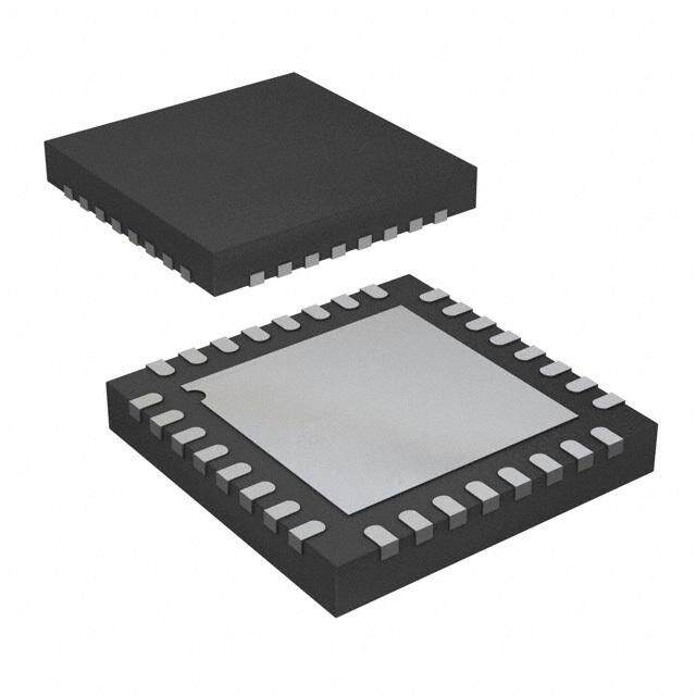
| 描述 | IC IF RCVR 11BIT 250MSPS 32LFCSP |
| 产品分类 | |
| 品牌 | Analog Devices Inc |
| 数据手册 | |
| 产品图片 |
|
| 产品型号 | AD6672BCPZ-250 |
| RF类型 | CDMA,LTE,W-CDMA,WiMAX |
| rohs | 无铅 / 符合限制有害物质指令(RoHS)规范要求 |
| 产品系列 | - |
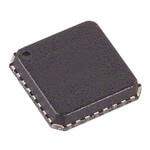
| 供应商器件封装 | 32-LFCSP-WQ(5x5) |
| 其它名称 | AD6672BCPZ250 |
| 功能 | IF 接收器 |
| 包装 | 托盘 |
| 封装/外壳 | 32-WFQFN 裸露焊盘,CSP |
| 标准包装 | 1 |
| 视频文件 | http://www.digikey.cn/classic/video.aspx?PlayerID=1364138032001&width=640&height=505&videoID=2245193150001 |
| 辅助属性 | 采样率达 250MSPS |
| 频率 | - |


- 商务部:美国ITC正式对集成电路等产品启动337调查
- 曝三星4nm工艺存在良率问题 高通将骁龙8 Gen1或转产台积电
- 太阳诱电将投资9.5亿元在常州建新厂生产MLCC 预计2023年完工
- 英特尔发布欧洲新工厂建设计划 深化IDM 2.0 战略
- 台积电先进制程称霸业界 有大客户加持明年业绩稳了
- 达到5530亿美元!SIA预计今年全球半导体销售额将创下新高
- 英特尔拟将自动驾驶子公司Mobileye上市 估值或超500亿美元
- 三星加码芯片和SET,合并消费电子和移动部门,撤换高东真等 CEO
- 三星电子宣布重大人事变动 还合并消费电子和移动部门
- 海关总署:前11个月进口集成电路产品价值2.52万亿元 增长14.8%


PDF Datasheet 数据手册内容提取
IF Receiver Data Sheet AD6672 FEATURES GENERAL DESCRIPTION 11-bit, 250 MSPS output data rate The AD6672 is an 11-bit intermediate receiver with sampling Performance with NSR enabled speeds of up to 250 MSPS. The AD6672 is designed to support SNR: 75.2 dBFS in a 55 MHz band to 185 MHz at 250 MSPS communications applications, where low cost, small size, wide SNR: 72.8 dBFS in an 82 MHz band to 185 MHz at 250 MSPS bandwidth, and versatility are desired. Performance with NSR disabled The ADC core features a multistage, differential pipelined SNR: 66.4 dBFS up to 185 MHz at 250 MSPS architecture with integrated output error correction logic. The SFDR: 87 dBc up to 185 MHz at 250 MSPS ADC features wide bandwidth inputs supporting a variety of Total power consumption: 358 mW at 250 MSPS user-selectable input ranges. An integrated voltage reference 1.8 V supply voltages eases design considerations. A duty cycle stabilizer is provided LVDS (ANSI-644 levels) outputs to compensate for variations in the ADC clock duty cycle, Integer 1-to-8 input clock divider (625 MHz maximum input) allowing the converters to maintain excellent performance. Internal ADC voltage reference Flexible analog input range The ADC core output is connected internally to a noise shaping 1.4 V p-p to 2.0 V p-p (1.75 V p-p nominal) requantizer (NSR) block. The device supports two output modes Serial port control that are selectable via the serial port interface (SPI). With the Energy saving power-down modes NSR feature enabled, the outputs of the ADCs are processed such that the AD6672 supports enhanced SNR performance within a APPLICATIONS limited region of the Nyquist bandwidth while maintaining an Communications 11-bit output resolution. The NSR block is programmed to provide Diversity radio and smart antenna (MIMO) systems a bandwidth of up to 33% of the sample clock. For example, with Multimode digital receivers (3G) a sample clock rate of 250 MSPS, the AD6672 can achieve up to WCDMA, LTE, CDMA2000 73.6 dBFS SNR for an 82 MHz bandwidth at 185 MHz f . IN WiMAX, TD-SCDMA With the NSR block disabled, the ADC data is provided directly I/Q demodulation systems to the output with an output resolution of 11 bits. The AD6672 General-purpose software radios can achieve up to 66.6 dBFS SNR for the entire Nyquist bandwidth when operated in this mode. FUNCTIONAL BLOCK DIAGRAM AVDD AGND DRVDD DCO± VIN+ 14 NOISE SHAPED 11 PIPELINE VIN– ADC REQU(NASNRT)IZER 0/D0± DATA VCM MULITIPLEXER AND LVDS DRIVERS AD6672 D9±/D10± OR± REFERENCE 1-TO-8 CLOCK SERIAL PORT DIVIDER SCLK SDIO CSB CLK+ CLK– 09997-001 Figure 1. Rev. C Document Feedback Information furnished by Analog Devices is believed to be accurate and reliable. However, no responsibility is assumed by Analog Devices for its use, nor for any infringements of patents or other One Technology Way, P.O. Box 9106, Norwood, MA 02062-9106, U.S.A. rights of third parties that may result from its use. Specifications subject to change without notice. No license is granted by implication or otherwise under any patent or patent rights of Analog Devices. Tel: 781.329.4700 ©2011–2014 Analog Devices, Inc. All rights reserved. Trademarks and registered trademarks are the property of their respective owners. Technical Support www.analog.com
AD6672 Data Sheet TABLE OF CONTENTS Features .............................................................................................. 1 Voltage Reference ....................................................................... 18 Applications ....................................................................................... 1 Clock Input Considerations ...................................................... 18 General Description ......................................................................... 1 Power Dissipation and Standby Mode .................................... 19 Functional Block Diagram .............................................................. 1 Digital Outputs ........................................................................... 20 Revision History ............................................................................... 2 ADC Overrange (OR) ................................................................ 20 Product Highlights ........................................................................... 3 Noise Shaping Requantizer ........................................................... 21 Specifications ..................................................................................... 4 22% BW NSR Mode (55 MHz BW at 250 MSPS) ..................... 21 ADC DC Specifications ............................................................... 4 33% BW NSR Mode (>82 MHz BW at 250 MSPS) ............... 21 ADC AC Specifications ............................................................... 5 Serial Port Interface (SPI) .............................................................. 23 Digital Specifications ................................................................... 7 Configuration Using the SPI ..................................................... 23 Switching Specifications .............................................................. 8 Hardware Interface ..................................................................... 23 Timing Specifications .................................................................. 9 SPI Accessible Features .............................................................. 24 Absolute Maximum Ratings .......................................................... 10 Memory Map .................................................................................. 25 Thermal Characteristics ............................................................ 10 Reading the Memory Map Register Table ............................... 25 ESD Caution ................................................................................ 10 Memory Map Register Table ..................................................... 26 Pin Configurations and Function Descriptions ......................... 11 Memory Map Register Description ......................................... 28 Typical Performance Characteristics ........................................... 12 Applications Information .............................................................. 29 Equivalent Circuits ......................................................................... 15 Design Guidelines ...................................................................... 29 Theory of Operation ...................................................................... 16 Outline Dimensions ....................................................................... 30 ADC Architecture ...................................................................... 16 Ordering Guide .......................................................................... 30 Analog Input Considerations .................................................... 16 REVISION HISTORY 12/14—Rev. B to Rev. C Changes to Features Section............................................................ 1 Changes to 33% BW NSR Mode (>82 MHz BW at 250 MSPS) Section .............................................................................................. 21 Changes to Reading the Memory Map Register Table Section .... 25 Changes to Table 13 ........................................................................ 26 Change to Memory Map Register Description Section............. 28 7/14—Rev. A to Rev. B Changes to Features Section and Figure 1 ..................................... 1 Changes to Full Power Bandwidth Parameter, Table 2 ................ 6 Deleted Noise Bandwidth Parameter, Table 2 ............................... 6 11/12—Rev. 0 to Rev. A Changes to Features Section............................................................ 1 7/11—Revision 0: Initial Version Rev. C | Page 2 of 30
Data Sheet AD6672 When the NSR block is disabled, the ADC data is provided directly PRODUCT HIGHLIGHTS to the output at a resolution of 11 bits. This allows the AD6672 1. Integrated 11-bit, 250 MSPS ADC with a noise shaping to be used in telecommunication applications, such as a digital requantizer option. predistortion observation path, where wider bandwidths are 2. Operation from a single 1.8 V supply and a separate digital required. output driver supply accommodating LVDS outputs. After digital signal processing, multiplexed output data is 3. On-chip 1-to-8 integer clock divider function to support a routed into one 11-bit output port such that the maximum data wide range of clocking. rate is 500 Mbps (DDR). This output is LVDS and supports 4. Noise shaping requantizer function allows attaining improved ANSI-644 levels. SNR within a reduced frequency band. With NSR enabled, the AD6672 supports up to 82 MHz at 250 MSPS. The AD6672 receiver digitizes a wide spectrum of IF frequencies. 5. Standard serial port interface (SPI) that supports various This IF sampling architecture greatly reduces component cost product features and functions, such as data formatting and complexity compared with traditional analog techniques or (offset binary, twos complement, or gray coding), enabling less integrated digital methods. the clock DCS, power-down, test modes, and voltage Flexible power-down options allow significant power savings. reference mode. Programming for device setup and control is accomplished using a 3-wire, SPI-compatible serial interface with numerous modes to support board level system testing. The AD6672 is available in a 32-lead, RoHS-compliant LFCSP and is specified over the industrial temperature range of −40°C to +85°C. This product is protected by a U.S. patent. Rev. C | Page 3 of 30
AD6672 Data Sheet SPECIFICATIONS ADC DC SPECIFICATIONS AVDD = 1.8 V, DRVDD = 1.8 V, maximum sample rate, VIN = −1.0 dBFS differential input, 1.75 V p-p full-scale input range, DCS enabled, unless otherwise noted. Table 1. Parameter Temperature Min Typ Max Unit RESOLUTION Full 11 Bits ACCURACY No Missing Codes Full Guaranteed Offset Error Full ±11 mV Gain Error Full +3/−6.5 % FSR Differential Nonlinearity (DNL) Full ±0.2 LSB 25°C ±0.1 LSB Integral Nonlinearity (INL)1 Full ±0.3 LSB 25°C ±0.12 LSB TEMPERATURE DRIFT Offset Error Full ±7 ppm/°C Gain Error Full ±85 ppm/°C INPUT-REFERRED NOISE VREF = 1.0 V 25°C 0.65 LSB rms ANALOG INPUT Input Span Full 1.75 V p-p Input Capacitance2 Full 5 pF Input Resistance Full 20 kΩ Input Common-Mode Voltage Full 0.9 V POWER SUPPLIES Supply Voltage AVDD Full 1.7 1.8 1.9 V DRVDD Full 1.7 1.8 1.9 V Supply Current I 1 Full 136 145 mA AVDD I 1 (NSR Disabled) Full 63 68 mA DRVDD I 1 (NSR Enabled, 22% Bandwidth Mode) Full 89 mA DRVDD I 1 (NSR Enabled, 33% Bandwidth Mode) Full 99 mA DRVDD POWER CONSUMPTION Sine Wave Input (DRVDD = 1.8 V, NSR Disabled) Full 358 385 mW Sine Wave Input (DRVDD = 1.8 V, NSR Enabled, mW 22% Bandwidth Mode) Full 405 Sine Wave Input (DRVDD = 1.8 V, NSR Enabled, mW 33% Bandwidth Mode) Full 423 Standby Power3 Full 50 mW Power-Down Power Full 5 mW 1 Measured with a low input frequency, full-scale sine wave, with approximately 5 pF loading on each output bit. 2 Input capacitance refers to the effective capacitance between one differential input pin and AGND. See Figure 18 for the equivalent analog input structure. 3 Standby power is measured with a dc input, the CLK pin inactive (set to AVDD or AGND). Rev. C | Page 4 of 30
Data Sheet AD6672 ADC AC SPECIFICATIONS AVDD = 1.8 V, DRVDD = 1.8 V, maximum sample rate, VIN = −1.0 dBFS differential input, 1.75 V p-p full-scale input range, unless otherwise noted. Table 2. Parameter1 Temperature Min Typ Max Unit SIGNAL-TO-NOISE-RATIO (SNR) NSR Disabled f = 30 MHz 25°C 66.6 dBFS IN f = 90 MHz 25°C 66.6 dBFS IN f = 140 MHz 25°C 66.5 dBFS IN f = 185 MHz 25°C 66.4 dBFS IN Full 65.4 dBFS f = 220 MHz 25°C 66.3 dBFS IN NSR Enabled 22% Bandwidth Mode f = 30 MHz 25°C 75.8 dBFS IN f = 90 MHz 25°C 75.7 dBFS IN f = 140 MHz 25°C 75.6 dBFS IN f = 185 MHz 25°C 75.2 dBFS IN Full 72.2 dBFS f = 220 MHz 25°C 74.8 dBFS IN 33% Bandwidth Mode f = 30 MHz 25°C 73.4 dBFS IN f = 90 MHz 25°C 73.3 dBFS IN f = 140 MHz 25°C 73.2 dBFS IN f = 185 MHz 25°C 72.8 dBFS IN Full 69.2 dBFS f = 220 MHz 25°C 72.4 dBFS IN SIGNAL-TO-NOISE RATIO AND DISTORTION (SINAD) f = 30 MHz 25°C 65.7 dBFS IN f = 90 MHz 25°C 65.7 dBFS IN f = 140 MHz 25°C 65.6 dBFS IN f = 185 MHz 25°C 65.3 dBFS IN Full 64.4 dBFS f = 220 MHz 25°C 65.2 dBFS IN WORST SECOND OR THIRD HARMONIC f = 30 MHz 25°C −88 dBc IN f = 90 MHz 25°C −88 dBc IN f = 140 MHz 25°C −89 dBc IN f = 185 MHz 25°C −87 dBc IN Full −80 dBc f = 220 MHz 25°C −88 dBc IN SPURIOUS-FREE DYNAMIC RANGE (SFDR) f = 30 MHz 25°C 88 dBc IN f = 90 MHz 25°C 88 dBc IN f = 140 MHz 25°C 89 IN f = 185 MHz 25°C 87 dBc IN Full 80 dBc f = 220 MHz 25°C 88 dBc IN Rev. C | Page 5 of 30
AD6672 Data Sheet Parameter1 Temperature Min Typ Max Unit WORST OTHER (HARMONIC OR SPUR) f = 30 MHz 25°C −96 dBc IN f = 90 MHz 25°C −97 dBc IN f = 140 MHz 25°C −97 dBc IN f = 185 MHz 25°C −98 dBc IN Full −81 dBc f = 220 MHz 25°C −97 dBc IN TWO-TONE SFDR f = 184.12 MHz, 187.12 MHz (−7 dBFS) 25°C 88 dBc IN FULL POWER BANDWIDTH 25°C 1000 MHz 1 See the AN-835 Application Note, Understanding High Speed ADC Testing and Evaluation, for a complete set of definitions. Rev. C | Page 6 of 30
Data Sheet AD6672 DIGITAL SPECIFICATIONS AVDD = 1.8 V, DRVDD = 1.8 V, maximum sample rate, VIN = −1.0 dBFS differential input, 1.0 V internal reference, DCS enabled, unless otherwise noted. Table 3. Parameter Temperature Min Typ Max Unit DIFFERENTIAL CLOCK INPUTS (CLK+, CLK−) Logic Compliance CMOS/LVDS/LVPECL Internal Common-Mode Bias Full 0.9 V Differential Input Voltage Full 0.3 3.6 V p-p Input Voltage Range Full AGND AVDD V Input Common-Mode Range Full 0.9 1.4 V High Level Input Current Full 10 +22 µA Low Level Input Current Full −22 −10 µA Input Capacitance Full 4 pF Input Resistance Full 12 15 18 kΩ LOGIC INPUT (CSB)1 High Level Input Voltage Full 1.22 2.1 V Low Level Input Voltage Full 0 0.6 V High Level Input Current Full 50 71 µA Low Level Input Current Full −5 +5 µA Input Resistance Full 26 kΩ Input Capacitance Full 2 pF LOGIC INPUT (SCLK)2 High Level Input Voltage Full 1.22 2.1 V Low Level Input Voltage Full 0 0.6 V High Level Input Current Full 45 70 µA Low Level Input Current Full −5 +5 µA Input Resistance Full 26 kΩ Input Capacitance Full 2 pF LOGIC INPUTS (SDIO)1 High Level Input Voltage Full 1.22 2.1 V Low Level Input Voltage Full 0 0.6 V High Level Input Current Full 45 70 µA Low Level Input Current Full −5 +5 µA Input Resistance Full 26 kΩ Input Capacitance Full 5 pF DIGITAL OUTPUTS (OR+, OR−) LVDS Data and OR Outputs Differential Output Voltage (V ), ANSI Mode Full 250 350 450 mV OD Output Offset Voltage (V ), ANSI Mode Full 1.15 1.25 1.35 V OS Differential Output Voltage (V ), Reduced Swing Mode Full 150 200 280 mV OD Output Offset Voltage (V ), Reduced Swing Mode Full 1.15 1.25 1.35 V OS 1 Pull-up. 2 Pull-down. Rev. C | Page 7 of 30
AD6672 Data Sheet SWITCHING SPECIFICATIONS Table 4. Parameter Temperature Min Typ Max Unit CLOCK INPUT PARAMETERS Input Clock Rate Full 625 MHz Conversion Rate1 Full 40 250 MSPS CLK Period—Divide-by-1 Mode (t ) Full 4 ns CLK CLK Pulse Width High (t ) CH Divide-by-1 Mode, DCS Enabled Full 1.8 2.0 2.2 ns Divide-by-1 Mode, DCS Disabled Full 1.9 2.0 2.1 ns Divide-by-2 Mode Through Divide-by-8 Mode Full 0.8 ns Aperture Delay (t ) Full 1.0 ns A Aperture Uncertainty (Jitter, t) Full 0.1 ps rms J DATA OUTPUT PARAMETERS Data Propagation Delay (t ) Full 4.1 4.7 5.2 ns PD DCO Propagation Delay (t ) Full 4.7 5.3 5.8 ns DCO DCO-to-Data Skew (t ) Full 0.3 0.5 0.7 ns SKEW Pipeline Delay (Latency)—NSR Disabled Full 10 Cycles Pipeline Delay (Latency)—NSR Enabled Full 13 Cycles Wake-Up Time (from Standby) Full 10 µs Wake-Up Time (from Power-Down) Full 100 µs Out-of-Range Recovery Time Full 3 Cycles 1 Conversion rate is the clock rate after the divider. Timing Diagram tA N – 1 N + 4 VIN N + 5 N N + 3 N + 1 N + 2 tCH tCLK CLK+ CLK– tDCO DCO– DCO+ tSKEW ODD/EVEN tPD 0/D0± 0 D0 0 D0 0 D0 0 D0 0 (LSB) N – 10 N – 10 N – 9 N – 9 N – 8 N – 8 N – 7 N – 7 N – 6 D9±(/MDS10B±) N D–9 10 ND –1 010 ND –9 9 ND 1–0 9 ND –9 8 ND 1–0 8 ND –9 7 ND 1–0 7 ND –9 6 09997-002 Figure 2. LVDS Data Output Timing Rev. C | Page 8 of 30
Data Sheet AD6672 TIMING SPECIFICATIONS Table 5. Parameter Test Conditions/Comments Min Typ Max Unit SPI TIMING REQUIREMENTS See Figure 42 for the SPI timing diagram t Setup time between the data and the rising edge of SCLK 2 ns DS t Hold time between the data and the rising edge of SCLK 2 ns DH t Period of the SCLK 40 ns CLK t Setup time between CSB and SCLK 2 ns S t Hold time between CSB and SCLK 2 ns H t Minimum period that SCLK should be in a logic high state 10 ns HIGH t Minimum period that SCLK should be in a logic low state 10 ns LOW t Time required for the SDIO pin to switch from an input to an output 10 ns EN_SDIO relative to the SCLK falling edge (not shown in Figure 42) t Time required for the SDIO pin to switch from an output to an input 10 ns DIS_SDIO relative to the SCLK rising edge (not shown in Figure 42) Rev. C | Page 9 of 30
AD6672 Data Sheet ABSOLUTE MAXIMUM RATINGS THERMAL CHARACTERISTICS Table 6. The exposed paddle must be soldered to the ground plane for the Parameter Rating LFCSP package. Soldering the exposed paddle to the customer Electrical board increases the reliability of the solder joints, maximizing AVDD to AGND −0.3 V to +2.0 V the thermal capability of the package. DRVDD to AGND −0.3 V to +2.0 V VIN+, VIN− to AGND −0.3 V to AVDD + 0.2 V Table 7. Thermal Resistance CLK+, CLK− to AGND −0.3 V to AVDD + 0.2 V Airflow VCM to AGND −0.3 V to AVDD + 0.2 V Velocity CSB to AGND −0.3 V to DRVDD + 0.3 V Package Type (m/sec) θ 1, 2 θ 1, 3 θ 1, 4 Unit JA JC JB SCLK to AGND −0.3 V to DRVDD + 0.3 V 32-Lead LFCSP 0 37.1 3.1 20.7 °C/W SDIO to AGND −0.3 V to DRVDD + 0.3 V 5 mm × 5 mm 1.0 32.4 °C/W (CP-32-12) 0/D0−, 0/D0 + Through D9−/D10−, −0.3 V to DRVDD + 0.3 V 2.0 29.1 °C/W D9+/D10+ to AGND OR+/OR− to AGND −0.3 V to DRVDD + 0.3 V 1 Per JEDEC 51-7, plus JEDEC 25-5 2S2P test board. 2 Per JEDEC JESD51-2 (still air) or JEDEC JESD51-6 (moving air). DCO+, DCO− to AGND −0.3 V to DRVDD + 0.3 V 3 Per MIL-Std 883, Method 1012.1. Environmental 4 Per JEDEC JESD51-8 (still air). Operating Temperature Range −40°C to +85°C (Ambient) Typical θ is specified for a 4-layer PCB with a solid ground JA Maximum Junction Temperature 150°C plane. As shown in Table 7, airflow increases heat dissipation, Under Bias which reduces θ . In addition, metal in direct contact with the JA Storage Temperature Range −65°C to +125°C package leads from metal traces—through holes, ground, and (Ambient) power planes—reduces the θ . JA Stresses at or above those listed under Absolute Maximum ESD CAUTION Ratings may cause permanent damage to the product. This is a stress rating only; functional operation of the product at these or any other conditions above those indicated in the operational section of this specification is not implied. Operation beyond the maximum operating conditions for extended periods may affect product reliability. Rev. C | Page 10 of 30
Data Sheet AD6672 PIN CONFIGURATIONS AND FUNCTION DESCRIPTIONS AVDDAVDDVIN+VIN–AVDDAVDDVCMDNC 21098765 33322222 CLK+ 1 24 CSB CLK– 2 23 SCLK AD6672 AVDD 3 22 SDIO INTERLEAVED OR– 4 21 DCO+ OR+ 5 LVDS 20 DCO– 0/D0– (LSB) 6 TOP VIEW 19 D9+/D10+ (MSB) (Not to Scale) 0/D0+ (LSB) 7 18 D9–/D10– (MSB) DRVDD 8 17 DRVDD 910111213141516 –+–+–+–+ 22446688 DDDDDDDD –/+/–/+/–/+/–/+/ D1D1D3D3D5D5D7D7 NOTES 1. THE EXPOSED THERMAL PADDLE ON THE BOTTOM OF THE 2.PPGDAANRCRCOKT U=.A N TNGDHOE IF S NPO OERRXTO PP VCROIODOSNEPENSED ERT PC HOATE.DP DAEDONRLAE AN LTMOOIOUTG NSC .TGO RBNOEN UECNCODTN TFNOOE RCT THTEIHSDE PTION. 09997-003 Figure 3. LFCSP Pin Configuration (Top View) Table 8. Pin Function Descriptions Pin No. Mnemonic Type Description ADC Power Supplies 8, 17 DRVDD Supply Digital Output Driver Supply (1.8 V Nominal). 3, 27, 28, 31, 32 AVDD Supply Analog Power Supply (1.8 V Nominal). 0 AGND, Ground Analog Ground. The exposed thermal paddle on the bottom of the package provides the Exposed Paddle analog ground for the part. This exposed paddle must be connected to ground for proper operation. 25 DNC Do Not Connect. Do not connect to this pin. ADC Analog 30 VIN+ Input Differential Analog Input Pin (+). 29 VIN− Input Differential Analog Input Pin (−). 26 VCM Output Common-Mode Level Bias Output for Analog Inputs. This pin should be decoupled to ground using a 0.1 μF capacitor. 1 CLK+ Input ADC Clock Input—True. 2 CLK− Input ADC Clock Input—Complement. Digital Outputs 5 OR+ Output Overrange indicator—True. 4 OR− Output Overrange indicator—Complement. 7 0/D0+ (LSB) Output DDR LVDS Output Data 0—True. The output bit on the rising edge of the data clock output (DCO) from this output is always a Logic 0 (see Figure 2). 6 0/D0− (LSB) Output DDR LVDS Output Data 0—Complement. The output bit on the rising edge of the data clock output (DCO) from this output is always a Logic 0 (see Figure 2). 10 D1+/D2+ Output DDR LVDS Output Data 1/2—True. 9 D1−/D2− Output DDR LVDS Output Data 1/2—Complement. 12 D3+/D4+ Output DDR LVDS Output Data 3/4—True. 11 D3−/D4− Output DDR LVDS Output Data 3/4—Complement. 14 D5+/D6+ Output DDR LVDS Output Data 5/6—True. 13 D5−/D6− Output DDR LVDS Output Data 5/6—Complement. 16 D7+/D8+ Output DDR LVDS Output Data 7/8—True. 15 D7−/D8− Output DDR LVDS Output Data 7/8—Complement. 19 D9+/D10+ (MSB) Output DDR LVDS Output Data 9/10—True. 18 D9−/D10− (MSB) Output DDR LVDS Output Data 9/10—Complement. 21 DCO+ Output LVDS Data Clock Output—True. 20 DCO− Output LVDS Data Clock Output—Complement. SPI Control 23 SCLK Input SPI Serial Clock. 22 SDIO Input/output SPI Serial Data I/O. 24 CSB Input SPI Chip Select (Active Low). Rev. C | Page 11 of 30
AD6672 Data Sheet TYPICAL PERFORMANCE CHARACTERISTICS AVDD = 1.8 V, DRVDD = 1.8 V, sample rate = 250 MSPS, DCS enabled, 1.75 V p-p differential input, VIN = −1.0 dBFS, 32k sample, T = 25°C, A unless otherwise noted. 0 0 250MSPS 250 MSPS 30.1MHz @ –1.0dBFS 185.1MHz @ –1.0dBFS –20 SNR = 65.6dB (66.6dBFS) –20 SNR = 65.4dB (66.4dBFS) SFDR = 88dBc SFDR = 87dBc –40 –40 S) S) F F B B DE (d –60 SECOND THIRD DE (d –60 THIRD SECOND LITU –80 HARMONIC HARMONIC LITU –80 HARMONIC HARMONIC P P M M A A –100 –100 –120 –120 –1400 10 20 30 40FR5E0QUE60NCY7 0(MH8z0) 90 100 110 120 09997-004 –1400 10 20 30 40FR5E0QUE60NCY7 0(MH8z0) 90 100 110 120 09997-007 Figure 4. Single-Tone FFT with fIN = 30.1 MHz Figure 7. Single-Tone FFT with fIN = 185.1 MHz 0 0 250MSPS 250 MSPS 90.1MHz @ –1.0dBFS 220.1MHz @ –1.0dBFS –20 SNR = 65.6dB (66.6dBFS) –20 SNR = 65.3dB (66.3dBFS) SFDR = 88dBc SFDR = 88dBc –40 –40 S) S) F F B B DE (d –60 THIRD SECOND DE (d –60 SECOND THIRD U HARMONIC HARMONIC U HARMONIC HARMONIC LIT –80 LIT –80 P P M M A A –100 –100 –120 –120 –1400 10 20 30 40FR5E0QUE60NCY7 0(MH8z0) 90 100 110 120 09997-005 –1400 10 20 30 40FR5E0QUE60NCY7 0(MH8z0) 90 100 110 120 09997-008 Figure 5. Single-Tone FFT with fIN = 90.1 MHz Figure 8. Single-Tone FFT with fIN = 220.1 MHz 0 0 250MSPS 250 MSPS 140.1MHz @ –1.0dBFS 305.1MHz @ –1.0dBFS –20 SNR = 65.5dB (66.5dBFS) –20 SNR = 64.8dB (65.8dBFS) SFDR = 89dBc SFDR = 82dBc –40 –40 S) S) F F B B DE (d –60 SECOND THIRD DE (d –60 THIRD SECOND U HARMONIC HARMONIC U HARMONIC HARMONIC LIT –80 LIT –80 P P M M A A –100 –100 –120 –120 –1400 10 20 30 40FR5E0QUE60NCY7 0(MH8z0) 90 100 110 120 09997-006 –1400 10 20 30 40FR5E0QUE60NCY7 0(MH8z0) 90 100 110 120 09997-009 Figure 6. Single-Tone FFT with fIN = 140.1 MHz Figure 9. Single-Tone FFT with fIN = 305.1 MHz Rev. C | Page 12 of 30
Data Sheet AD6672 120 0 100 –20 SFDR (dBc) BFS) SFDR (dBFS) BFS) IMD3 (dBc) FDR (dBc and d 8600 SNR (dBFS) MD3 (dBc and d ––4600 SNR/S 40 SFDR (dBc) SFDR/I –80 SFDR (dBFS) SNR (dBc) 20 –100 IMD3 (dBFS) –0100 –90 –80 –I7N0PUT–6A0MPL–5IT0UDE–4 (0dBF–S3)0 –20 –10 0 09997-010 –12–090.0 –78.5 –67I.N0PUT–A5M5.P5LITU–D44E. 0(dBF–S3)2.5 –21.0 –9.509997-013 Figure 10. Single-Tone SNR/SFDR vs. Input Amplitude (AIN) Figure 13. Two-Tone SFDR/IMD3 vs. Input Amplitude (AIN) with fIN = 90.1 MHz, fS = 250 MSPS with fIN1 = 184.12 MHz, fIN2 = 187.12 MHz, fS = 250 MSPS 100 0 250MSPS 89.12MHz @ –7.0dBFS 95 –20 92.12MHz @ –7.0dBFS SFDR (dBFS) SFDR = 87dBc (94dBFS) S) 90 DR (dBc and dBF 8850 LITUDE (dBFS) –––468000 SF 75 MP R/ A N –100 S 70 SNR (dBc) 65 –120 6060 75 90 105 120 135 150F165RE180QU195EN210CY 225(MH240z)255270 285 300 315 330345 09997-011 –1400 10 20 30 40 FR50EQU6E0NC7Y0 (Hz8)0 90 100 110 120 09997-014 Figure 11. Single-Tone SNR/SFDR vs. Input Frequency (fIN), fS = 250 MSPS Figure 14. Two-Tone FFT with fIN1 = 89.12 MHz, fIN2 = 92.12 MHz 0 0 250MSPS 184.12MHz @ –7.0dBFS –20 187.12MHz @ –7.0dBFS –20 SFDR (dBc) SFDR = 86dBc (93dBFS) S) dBF –40 IMD3 (dBc) S) –40 D3 (dBc and –60 LITUDE (dBF ––6800 M P FDR/I –80 SFDR (dBFS) AM –100 S –100 –120 IMD3 (dBFS) –120–90 –80 –70 INP–U6T0AMP–L5I0TUDE– 4(d0BFS–)30 –20 –10 09997-012 –1400 10 20 30 40 FR50EQU6E0NC7Y0 (Hz8)0 90 100 110 120 09997-015 Figure 12. Two-Tone SFDR/IMD3 vs. Input Amplitude (AIN) Figure 15. Two-Tone FFT with fIN1 = 184.12 MHz, fIN2 = 187.12 MHz with fIN1 = 89.12 MHz, fIN2 = 92.12 MHz, fS = 250 MSPS Rev. C | Page 13 of 30
AD6672 Data Sheet 100 1000 0.65LSB RMS SFDR (dBc) 9000 16384 TOTAL HITS 95 8000 S) 90 BF 7000 d S nd 85 HIT6000 dBc a 80 R OF 5000 R ( BE D M4000 F 75 U R/S N3000 N S 70 SNR (dBFS) 2000 65 1000 6040 60 80 100SA1M20PLE1 R40ATE1 6(M0SP1S8)0 200 220 240 09997-016 0 OUNTPUT CODE N – 1 09997-017 Figure 16. Single-Tone SNR/SFDR vs. Sample Rate (fS) with fIN = 90 MHz Figure 17. Grounded Input Histogram, fS = 250 MSPS Rev. C | Page 14 of 30
Data Sheet AD6672 EQUIVALENT CIRCUITS DRVDD AVDD VIN 350Ω SDIO 09997-018 26kΩ 09997-021 Figure 18. Equivalent Analog Input Circuit Figure 21. Equivalent SDIO Circuit AVDD AVDD AVDD 0.9V 350Ω SCLK 15kΩ 15kΩ CLK+ CLK– 26kΩ 09997-019 09997-022 Figure 19. Equivalent Clock Input Circuit Figure 22. Equivalent SCLK Input Circuit DRVDD AVDD 26kΩ 350Ω V+ V– CSB DATAOUT– DATAOUT+ V– V+ 09997-020 09997-023 Figure 20. Equivalent LVDS Output Circuit Figure 23. Equivalent CSB Input Circuit Rev. C | Page 15 of 30
AD6672 Data Sheet THEORY OF OPERATION The AD6672 can sample any f/2 frequency segment from dc to A small resistor in series with each input can help reduce the S 250 MHz using appropriate low-pass or band-pass filtering at peak transient current required from the output stage of the the ADC inputs with little loss in ADC performance. driving source. A shunt capacitor can be placed across the inputs to provide dynamic charging currents. This passive Programming and control of the AD6672 are accomplished network creates a low-pass filter at the ADC input; therefore, using a 3-pin, SPI-compatible serial interface. the precise values are dependent on the application. ADC ARCHITECTURE In intermediate frequency (IF) undersampling applications, the The AD6672 architecture consists of a front-end sample-and- shunt capacitors should be reduced. In combination with the hold circuit, followed by a pipelined switched-capacitor ADC. driving source impedance, the shunt capacitors limit the input The quantized outputs from each stage are combined into a bandwidth. Refer to the AN-742 Application Note, Frequency final 11-bit result in the digital correction logic. The pipelined Domain Response of Switched-Capacitor ADCs; the AN-827 architecture permits the first stage to operate on a new input Application Note, A Resonant Approach to Interfacing Amplifiers sample and the remaining stages to operate on the preceding to Switched-Capacitor ADCs; and the Analog Dialogue article, samples. Sampling occurs on the rising edge of the clock. “Transformer-Coupled Front-End for Wideband A/D Converters,” Each stage of the pipeline, excluding the last, consists of a low for more information on this subject. resolution flash ADC connected to a switched-capacitor digital- BIAS to-analog converter (DAC) and an interstage residue amplifier S S (MDAC). The MDAC magnifies the difference between the CS CFB reconstructed DAC output and the flash input for the next stage VIN+ in the pipeline. One bit of redundancy is used in each stage to CPAR1 CPAR2 facilitate digital correction of flash errors. The last stage simply H S S consists of a flash ADC. The input stage of the AD6672 contains a differential sampling CS VIN– ceenrirrdcouerdist, mtahnoaddt epcsaa.ns Ts behsee t aohcue- t doparu ttda cs tt-oac gotihunepg lo ebudlto picnuk td abilfuifgefnfreesrn tsth.i Tea lhd oear to asu,i nctpgoulrert- ects CPAR1 S CPAR2 BIAS S CFB 09997-024 Figure 24. Switched-Capacitor Input buffers are powered from a separate supply, allowing digital output noise to be separated from the analog core. During For best dynamic performance, match the source impedances power-down, the output buffers go into a high impedance state. driving VIN+ and VIN− and differentially balance the inputs. The AD6672 features a noise shaping requantizer (NSR) to Input Common Mode allow higher than 11-bit SNR to be maintained in a subset of The analog inputs of the AD6672 are not internally dc biased. the Nyquist band. In ac-coupled applications, the user must provide this bias ANALOG INPUT CONSIDERATIONS externally. Setting the device so that V = 0.5 × AVDD (or CM 0.9 V) is recommended for optimum performance. An on- The analog input to the AD6672 is a differential switched- board common-mode voltage reference is included in the capacitor circuit that has been designed to attain optimum design and is available from the VCM pin. Using the VCM performance when processing a differential input signal. output to set the input common mode is recommended. The clock signal alternatively switches the input between Optimum performance is achieved when the common-mode sample mode and hold mode (see the configuration shown in voltage of the analog input is set by the VCM pin voltage Figure 24). When the input is switched into sample mode, the (typically 0.5 × AVDD). The VCM pin must be decoupled to signal source must be capable of charging the sampling ground by a 0.1 µF capacitor, as described in the Applications capacitors and settling within 1/2 clock cycle. Information section. Place this decoupling capacitor close to the pin to minimize the series resistance and inductance between the part and this capacitor. Rev. C | Page 16 of 30
Data Sheet AD6672 Differential Input Configurations the true SNR performance of the AD6672. For applications where SNR is a key parameter, differential double balun coupling is Optimum performance can be achieved when driving the AD6672 the recommended input configuration (see Figure 28). In this in a differential input configuration. For baseband applications, the configuration, the input is ac-coupled and the VCM voltage is AD8138, ADA4937-1, and ADA4930-1 differential drivers provide provided to the input through a 33 Ω resistor. This resistor excellent performance and a flexible interface to the ADC. compensates for losses in the input baluns to provide a 50 Ω The output common-mode voltage of the ADA4930-1 is easily impedance to the driver. set with the VCM pin of the AD6672 (see Figure 25), and the In the double balun and transformer configurations, the value driver can be configured in a Sallen-Key filter topology to of the input capacitors and resistors is dependent on the input provide band-limiting of the input signal. frequency and source impedance. Based on these parameters, 15pF the value of the input resistors and capacitors may need to be 200Ω adjusted or some components may need to be removed. Table 9 33Ω 15Ω VIN 76.8Ω 90Ω VIN– AVDD displays recommended values to set the RC network for 5pF different input frequency ranges. However, these values are ADA4930-1 ADC dependent on the input signal and bandwidth and should be 0.1µF 33Ω 15Ω 120Ω VIN+ VCM used only as a starting guide. Note that the values given in Table 9 15pF are for each R1, R2, C2, and R3 component shown in Figure 26 200Ω and Figure 28. 0.1µF 09997-025 Table 9. Example RC Network Figure 25. Differential Input Configuration Using the ADA4930-1 Frequency R1 C1 R2 C2 R3 Range Series Differential Series Shunt Shunt For baseband applications where SNR is a key parameter, (MHz) (Ω) (pF) (Ω) (pF) (Ω) differential transformer coupling is the recommended input 0 to 100 33 8.2 0 15 49.9 configuration. An example is shown in Figure 26. To bias the 100 to 300 15 3.9 0 8.2 49.9 analog input, connect the VCM voltage to the center tap of the secondary winding of the transformer. An alternative to using a transformer-coupled input at C2 frequencies in the second Nyquist zone is to use an amplifier R3 with variable gain. The AD8375 digital variable gain amplifier R2 VIN+ (DVGA) provides good performance for driving the AD6672. R1 2V p-p 49.9Ω C1 ADC Figure 27 shows an example of the AD8375 driving the AD6672 through a band-pass antialiasing filter. R1 R2 VIN– VCM 1000pF 180nH 220nH 0.1µF C2 R3 0.1µF 09997-026 AD83751µH VPOS 301Ω 5.1pF 3.196p5FΩ V1C5pMF AD6672 Figure 26. Differential Transformer-Coupled Configuration 165Ω 2.5kΩ║2pF 1µH 1nF 1nF The signal characteristics must be considered when selecting a 68nH transformer. Most RF transformers saturate at frequencies 1000pF 180nH 220nH NOTES below a few megahertz. Excessive signal power can also cause 1.ALL INDUCTORSARE COILCRAFT® 0603CS COMPONENTS cAotr ien spauttu frraetqioune,n wciheisc hin l ethade ss etoco dnidst oNrytiqouni.s t zone and above, the 2 . FWCIELITTNHET RETRHVEEAD LEUAXETCS E1 4PS0THMIOOHWNz. NOAF RTEH EF O1RµH A C 2H0MOKHEz BINADNUDCWTOIDRTSH (F0I6L0T3ELRS). 09997-027 Figure 27. Differential Input Configuration Using the AD8375 noise performance of most amplifiers is not adequate to achieve C2 R3 0.1µF 0.1µF R1 R2 VIN+ 2V p-p 33Ω PA S S P C1 ADC 33Ω 0.1µF 0.1µF R1 R2 VIN– VCM C2 R3 0.1µF 09997-028 Figure 28. Differential Double Balun Input Configuration Rev. C | Page 17 of 30
AD6672 Data Sheet VOLTAGE REFERENCE A stable and accurate voltage reference is built into the AD6672. 25Ω ADC 390pF 390pF The full-scale input range can be adjusted by varying the CILNOPCUKT CLK+ reference voltage via SPI. The input span of the ADC tracks 390pF reference voltage changes linearly. 1nF CLK– CLOCK INPUT CONSIDERATIONS 25Ω SHDCSIHMOOSDT2ET8SK2:2Y 09997-044 For optimum performance, the AD6672 sample clock inputs, Figure 31. Balun-Coupled Differential Clock (Up to 625 MHz) CLK+ and CLK−, should be clocked with a differential signal. If a low jitter clock source is not available, another option is to The signal is typically ac-coupled into the CLK+ and CLK− pins ac-couple a differential PECL signal to the sample clock input via a transformer or via capacitors. These pins are biased pins as shown in Figure 32. The AD9510, AD9511, AD9512, internally (see Figure 29) and require no external bias. If the AD9513, AD9514, AD9515, AD9516, AD9517, AD9518, AD9520, inputs are floated, the CLK− pin is pulled low to prevent AD9522, AD9523, AD9524, and ADCLK905/ADCLK907/ spurious clocking. ADCLK925 clock drivers offer excellent jitter performance. AVDD 0.1µF 0.1µF ADC 0.9V CLOCK CLK+ INPUT AD95xx, CLK+ CLK– ADCLK9xx 100Ω 0.1µF PECL DRIVER 0.1µF CLOCK CLK– 4pF 4pF 09997-029 INPUT50kFΩigure 325. 0DkiΩfferential PE2C4L0 ΩSample C2l4o0cΩk (Up to 625 MHz) 09997-032 Figure 29. Simplified Equivalent Clock Input Circuit A third option is to ac-couple a differential LVDS signal to the Clock Input Options sample clock input pins, as shown in Figure 33. The AD9510, The AD6672 has a very flexible clock input structure. Clock AD9511, AD9512, AD9513, AD9514, AD9515, AD9516, input can be a CMOS, LVDS, LVPECL, or sine wave signal. AD9517, AD9518, AD9520, AD9522, AD9523, and AD9524 Regardless of the type of signal being used, clock source jitter is clock drivers offer excellent jitter performance. of the most concern, as described in the Jitter Considerations section. 0.1µF 0.1µF ADC CLOCK CLK+ Figure 30 and Figure 31 show two preferable methods for INPUT clocking the AD6672 (at clock rates of up to 625 MHz). A low AD95xx 100Ω 0.1µF LVDS DRIVER 0.1µF jitter clock source is converted from a single-ended signal to a CLOCK CLK– dTihffee RreFn btiaallu sni gcnoanlf iugsuirnagti oann iRs Fre bcaolmunm oern dReFd tfroarn cslfoocrkm freerq. uencies INPUT50kΩ 50kΩ 09997-033 Figure 33. Differential LVDS Sample Clock (Up to 625 MHz) between 125 MHz and 625 MHz, and the RF transformer is Input Clock Divider recommended for clock frequencies from 10 MHz to 250 MHz. The back-to-back Schottky diodes across the secondary The AD6672 contains an input clock divider with the ability to winding of the transformer limit clock excursions into the divide the input clock by integer values between 1 and 8. For AD6672 to approximately 0.8 V p-p differential. This limit helps divide ratios other than 1, the duty cycle stabilizer (DCS) is prevent the large voltage swings of the clock from feeding enabled by default on power-up. through to other portions of the AD6672 while preserving the fast rise and fall times of the signal, which are critical for low jitter performance. Mini-Circuits® ADT1-1WT, 1:1Z ADC 390pF 390pF CLOCK XFMR CLK+ INPUT 50Ω 100Ω 390pF CLK– SHDCSIHMOOSDT2ET8SK2:2Y 09997-043 Figure 30. Transformer-Coupled Differential Clock (Up to 250 MHz) Rev. C | Page 18 of 30
Data Sheet AD6672 Clock Duty Cycle In cases where aperture jitter may affect the dynamic range of the AD6672, treat the clock input as an analog signal. In addition, Typical high speed ADCs use both clock edges to generate a use separate power supplies for the clock drivers and the ADC variety of internal timing signals and, as a result, may be output driver to avoid modulating the clock signal with digital sensitive to clock duty cycle. Commonly, a ±5% tolerance is noise. Low jitter, crystal controlled oscillators provide the best required on the clock duty cycle to maintain dynamic clock sources. If the clock is generated from another type of performance characteristics. source (by gating, dividing, or another method), it should be The AD6672 contains a DCS that retimes the nonsampling retimed by the original clock during the last step. (falling) edge, providing an internal clock signal with a nominal Refer to the AN-501 Application Note, Aperture Uncertainty and 50% duty cycle. This allows the user to provide a wide range of ADC System Performance, and the AN-756 Application Note, clock input duty cycles without affecting the performance of the Sampled Systems and the Effects of Clock Phase Noise and Jitter, for AD6672. more information about jitter performance as it relates to ADCs. Jitter on the rising edge of the input clock is still of paramount POWER DISSIPATION AND STANDBY MODE concern and is not reduced by the duty cycle stabilizer. The duty cycle control loop does not function for clock rates less As shown in Figure 35, the power dissipated by the AD6672 is than 40 MHz nominally. The loop has a time constant proportional to its sample rate. The data in Figure 35 was taken associated with it that must be considered when the clock rate using the same operating conditions as those used for the may change dynamically. A wait time of 1.5 µs to 5 µs is Typical Performance Characteristics section. required after a dynamic clock frequency increase or decrease 0.40 0.25 before the DCS loop is relocked to the input signal. During the time that the loop is not locked, the DCS loop is bypassed, and 0.20 internal device timing is dependent on the duty cycle of the 0.30 idennispaaubbtll iecn lgtoh ctekh des uiDgtnyC acSly. ccIinlrec ssuutiact bhisi la irpzeepcrlo.i cmIanmt iaoellnn osd,t ehitde m rt oaa pymp baliexc iaamtpipoizrneos pa, cri ate to OWER (W) 0.20 TOTAL POWER 0.15 URRENT (A) P C performance. OTAL IAVDD 0.10 PPLY Jitter Considerations T U S 0.10 High speed, high resolution ADCs are sensitive to the quality of 0.05 the clock input. The degradation in SNR at a given input IDRVDD frequency (f ) due to jitter (t) can be calculated by SNRHF =IN −10 log[(2π × fIJN × tJRMS)2 + 10(−SNRLF/10)] 040 55 70 85 E10N0CO11D5E 1F3R0E1Q4U5E1N6C0Y1 (7M5S1P9S0)2052202352500 09997-035 In the equation, the rms aperture jitter represents the root-mean- Figure 35. AD6672-250 Power and Current vs. Sample Rate square of all jitter sources, which include the clock input, the By setting the internal power-down mode bits (Bits[1:0]) in the analog input signal, and the ADC aperture jitter specification. power modes register (Address 0x08) to 01, the AD6672 is IF undersampling applications are particularly sensitive to jitter, placed in power-down mode. In this state, the ADC typically as shown in Figure 34. dissipates 2.5 mW. During power-down, the output drivers are 80 placed in a high impedance state. 0.05ps 0.2ps Low power dissipation in power-down mode is achieved by 0.5ps 75 1ps shutting down the reference, reference buffer, biasing networks, 1.5ps MEASURED and clock. Internal capacitors are discharged when entering 70 power-down mode and then must be recharged when returning S) BF to normal operation. As a result, the wake-up time is related to R (d65 the time spent in power-down mode, and shorter power-down N S cycles result in proportionally shorter wake-up times. 60 When using the SPI port interface, the user can place the ADC 55 in power-down mode or standby mode. Standby mode allows the user to keep the internal reference circuitry powered when 501 IN1P0UT FREQUENCY (M10H0z) 1k09997-034 fmasotdeer , wseatk teh-eu pin ttiemrneasl a proe wreeqr-udiroewdn. T mo opduet tbhiets p (aBritt isn[t1o:0 s]t)a nind bthy e power modes register (Address 0x08) to 10. See the Memory Map Figure 34. SNR vs. Input Frequency and Jitter section and the AN-877 Application Note, Interfacing to High Speed ADCs via SPI, for additional details. Rev. C | Page 19 of 30
AD6672 Data Sheet DIGITAL OUTPUTS are available one propagation delay (t ) after the rising edge of PD the clock signal. The AD6672 output drivers can be configured for either ANSI LVDS or reduced swing LVDS using a 1.8 V DRVDD supply. Minimize the length of the output data lines as well as the loads placed on these lines to reduce transients within the AD6672. As detailed in the AN-877 Application Note, Interfacing to High These transients may degrade converter dynamic performance. Speed ADCs via SPI, the data format can be selected for offset binary, twos complement, or gray code when using the SPI The lowest typical conversion rate of the AD6672 is 40 MSPS. At control. clock rates below 40 MSPS, dynamic performance may degrade. Digital Output Enable Function (OEB) Data Clock Output (DCO) The AD6672 has a flexible three-state ability for the digital The AD6672 also provides the data clock output (DCO) output pins. The three-state mode is enabled using the SPI intended for capturing the data in an external register. Figure 2 interface. The data outputs can be three-stated by using the shows a timing diagram of the AD6672 output modes. output enable bar bit (Bit 4) in Register 0x14. This OEB ADC OVERRANGE (OR) function is not intended for rapid access to the data bus. The ADC overrange indicator is asserted when an overrange is Timing detected on the input of the ADC. The overrange condition is The AD6672 provides latched data with a pipeline delay of determined at the output of the ADC pipeline and, therefore, is 10 input sample clock cycles when NSR is disabled and provides subject to a latency of 10 ADC clock cycles. An overrange at the 13 input sample clock cycles when NSR is enabled. Data outputs input is indicated by this bit 10 clock cycles after it occurs. Table 10. Output Data Format VIN+ − VIN−, Input (V) Input Span = 1.75 V p-p (V) Offset Binary Output Mode Twos Complement Mode (Default) OR VIN+ − VIN− <−0.875 000 0000 0000 100 0000 0000 1 VIN+ − VIN− −0.875 000 0000 0000 100 0000 0000 0 VIN+ − VIN− 0 100 0000 0000 000 0000 0000 0 VIN+ − VIN− +0.875 111 1111 1111 011 1111 1111 0 VIN+ − VIN− >+0.875 111 1111 1111 011 1111 1111 1 Rev. C | Page 20 of 30
Data Sheet AD6672 NOISE SHAPING REQUANTIZER The AD6672 features a noise shaping requantizer (NSR) to 0 250MSPS allow more than an 11-bit SNR to be maintained in a subset of 180.1MHz @ –1.6BFS –20 SNR = 73.4dB (75.0dBFS) the Nyquist band. The harmonic performance of the receiver is SFDR = 93dBc (IN BAND) unaffected by the NSR feature. When enabled, the NSR contributes –40 an additional 0.6 dB of loss to the input signal, such that a FS) B 0 dBFS input is reduced to −0.6 dBFS at the output pins. E (d –60 D U Two bandwidth (BW) modes are provided; the mode can be LIT –80 selected from the SPI port. In each mode, the center frequency MP A of the band can be tuned such that IFs can be placed anywhere –100 in the Nyquist band. –120 22% BW NSR MODE (55 MHz BW AT 250 MSPS) Tovheer f2ir2s%t b oafn tdhwe iAdtDhC m soadmep oleff rearste e (x4c4e%lle onft tnhoei sNe ypqeurifsotr bmaanndc)e –1400 25 FR5E0QUENCY (M75Hz) 100 125 09997-037 and can be centered by setting the NSR mode bits (Bits[3:1]) in Figure 37. 22% Bandwidth Mode, Tuning Word = 28 the NSR control register (Address 0x3C) to 000. In this mode, 0 250MSPS the useful frequency range can be set using the 6-bit tuning 180.1MHz @ –1.6BFS –20 SNR = 73.3dB (74.9dBFS) word (Bits[5:0]) in the NSR tuning register (Address 0x3E). SFDR = 92dBc (IN BAND) There are 57 possible tuning words (TW); each step is 0.5% of –40 the ADC sample rate. The following equations describe the left S) F B band edge (f0), the channel center (fCENTER), and the right band E (d –60 edge (f1), respectively: UD LIT –80 f = f × 0.005 × TW P 0 ADC M A f = f + 0.11 × f –100 CENTER 0 ADC f1 = f0 + 0.22 × fADC –120 Figure 36 to Figure 38 show the typical spectrum that can be tehxrpeeec ttuedn ifnrog mw othrdes A. D6672 in the 22% bandwidth mode for –1400 25 FR5E0QUENCY (M75Hz) 100 125 09997-038 Figure 38. 22% Bandwidth Mode, Tuning Word = 41 0 250MSPS 33% BW NSR MODE (>82 MHZ BW AT 250 MSPS) 180.1MHz @ –1.6BFS –20 SNR = 73.4dB (75.0dBFS) SFDR = 92dBc (IN BAND) The second bandwidth mode offers excellent noise performance –40 over 33% of the ADC sample rate (66% of the Nyquist band) S) F and can be centered by setting the NSR mode bits in the NSR B E (d –60 control register (Address 0x3C) to 001. In this mode, the useful D U frequency range can be set using the 6-bit tuning word (TW) in LIT –80 P the NSR tuning register (Address 0x3E). There are 34 possible M A–100 tuning words; each step is 0.5% of the ADC sample rate. The following three equations describe the left band edge (f), the 0 –120 channel center (f ), and the right band edge (f), CENTER 1 respectively: –1400 25 FR5E0QUENCY (M75Hz) 100 125 09997-036 f0 = fADC × 0.005 × TW Figure 36. 22% Bandwidth Mode, Tuning Word = 13 fCENTER = f0 + 0.165 × fADC f = f + 0.33 × f 1 0 ADC Figure 39 to Figure 41 show the typical spectrum that can be expected from the AD6672 with the 33% bandwidth NSR mode enabled for three filter settings. Rev. C | Page 21 of 30
AD6672 Data Sheet 0 0 250MSPS 250MSPS 180.1MHz @ –1.6BFS 180.1MHz @ –1.6BFS –20 SNR = 71.1dB (72.7dBFS) –20 SNR = 70.9dB (72.5dBFS) SFDR = 92dBc (IN BAND) SFDR = 92dBc (IN BAND) –40 –40 S) S) F F B B E (d –60 E (d –60 D D U U LIT –80 LIT –80 P P M M A A –100 –100 –120 –120 –1400 25 FR5E0QUENCY (M75Hz) 100 125 09997-039 –1400 25 FR5E0QUENCY (M75Hz) 100 125 09997-041 Figure 39. 33% Bandwidth Mode, Tuning Word = 5 Figure 41. 33% Bandwidth Mode, Tuning Word = 27 0 250MSPS 180.1MHz @ –1.6BFS –20 SNR = 71.2dB (72.8dBFS) SFDR = 92dBc (IN BAND) –40 S) F B E (d –60 D U LIT –80 P M A –100 –120 –1400 25 FR5E0QUENCY (M75Hz) 100 125 09997-040 Figure 40. 33% Bandwidth Mode, Tuning Word = 17 Rev. C | Page 22 of 30
Data Sheet AD6672 SERIAL PORT INTERFACE (SPI) The AD6672 serial port interface (SPI) allows the user to All data is composed of 8-bit words. The first bit of each configure the converter for specific functions or operations individual byte of serial data indicates whether a read or write through a structured register space provided inside the ADC. command is issued. This allows the serial data input/output The SPI offers added flexibility and customization, depending (SDIO) pin to change direction from an input to an output. on the application. Addresses are accessed via the serial port In addition to word length, the instruction phase determines and can be written to or read from via the port. Memory is whether the serial frame is a read or write operation, allowing organized into bytes that can be further divided into fields. the serial port to be used both to program the chip and to read These fields are documented in the Memory Map section. For the contents of the on-chip memory. If the instruction is a detailed operational information, see the AN-877 Application readback operation, performing a readback causes the serial Note, Interfacing to High Speed ADCs via SPI. data input/output (SDIO) pin to change direction from an input CONFIGURATION USING THE SPI to an output at the appropriate point in the serial frame. Three pins define the SPI of this ADC: the SCLK pin, the Data can be sent in MSB first mode or in LSB first mode. MSB SDIO pin, and the CSB pin (see Table 11). The SCLK (serial first mode is the default on power-up and can be changed via clock) pin is used to synchronize the read and write data the SPI port configuration register. For more information about presented from and to the ADC. The SDIO (serial data this and other features, see the AN-877 Application Note, input/output) pin is a dual-purpose pin that allows data to be Interfacing to High Speed ADCs via SPI. sent and read from the internal ADC memory map registers. HARDWARE INTERFACE The CSB (chip select bar) pin is an active low control that The pins described in Table 11 comprise the physical interface enables or disables the read and write cycles. between the user programming device and the serial port of the Table 11. Serial Port Interface Pins AD6672. The SCLK pin and the CSB pin function as inputs Pin Function when using the SPI interface. The SDIO pin is bidirectional, SCLK Serial clock. The serial shift clock input, which is used to functioning as an input during write phases and as an output synchronize serial interface reads and writes. during readback. SDIO Serial data input/output. A dual-purpose pin that The SPI interface is flexible enough to be controlled by either typically serves as an input or an output, depending on the instruction being sent and the relative position in the FPGAs or microcontrollers. One method for SPI configuration timing frame. is described in detail in the AN-812 Application Note, Micro- CSB Chip select bar. An active low control that gates the read controller-Based Serial Port Interface (SPI) Boot Circuit. and write cycles. The SPI port should not be active during periods when the full dynamic performance of the converter is required. Because the SCLK signal, the CSB signal, and the SDIO signal are typically The falling edge of CSB, in conjunction with the rising edge of asynchronous to the ADC clock, noise from these signals can SCLK, determines the start of the framing. An example of the degrade converter performance. If the on-board SPI bus is used serial timing and its definitions can be found in Figure 42 and for other devices, it may be necessary to provide buffers Table 5. between this bus and the AD6672 to prevent these signals from Other modes involving the CSB are available. The CSB can be transitioning at the converter inputs during critical sampling held low indefinitely, which permanently enables the device; periods. this is called streaming. The CSB can stall high between bytes to allow for additional external timing. When CSB is tied high, SPI functions are placed in a high impedance mode. This mode turns on any SPI pin secondary functions. During an instruction phase, a 16-bit instruction is transmitted. Data follows the instruction phase, and its length is determined by the W0 and W1 bits. Rev. C | Page 23 of 30
AD6672 Data Sheet SPI ACCESSIBLE FEATURES Table 12 provides a brief description of the general features that are accessible via the SPI. These features are described in detail in the AN-877 Application Note, Interfacing to High Speed ADCs via SPI. The AD6672 part-specific features are described in the Memory Map Register Description section. Table 12. Features Accessible Using the SPI Feature Name Description Mode Allows the user to set either power-down mode or standby mode Clock Allows the user to access the DCS via the SPI Offset Allows the user to digitally adjust the converter offset Test I/O Allows the user to set test modes to have known data on output bits Output Mode Allows the user to set up outputs Output Phase Allows the user to set the output clock polarity Output Delay Allows the user to vary the DCO delay VREF Allows the user to set the reference voltage Digital Processing Allows the user to enable the synchronization features tDS tHIGH tCLK tH tS tDH tLOW CSB SCLK DON’T CARE DON’T CARE SDIO DON’T CARE R/W W1 W0 A12 A11 A10 A9 A8 A7 D5 D4 D3 D2 D1 D0 DON’T CARE 09997-042 Figure 42. Serial Port Interface Timing Diagram Rev. C | Page 24 of 30
Data Sheet AD6672 MEMORY MAP Default Values READING THE MEMORY MAP REGISTER TABLE After the AD6672 is reset, critical registers are loaded with Each row in the memory map register table has eight bit locations. default values. The default values for the registers are given in The memory map is roughly divided into four sections: the chip the memory map register table (Table 13). configuration registers (Address 0x00 to Address 0x02); the transfer register (Address 0xFF); the ADC functions registers, including Logic Levels setup, control, and test (Address 0x08 to Address 0x20); and the An explanation of logic level terminology follows: digital feature control registers (Address 0x3C and Address 0x3E). • “Bit is set” is synonymous with “bit is set to Logic 1” or The memory map register table (Table 13) documents the “writing Logic 1 for the bit.” default hexadecimal value for each hexadecimal address shown. • “Clear a bit” is synonymous with “bit is set to Logic 0” or The Bit 7 (MSB) column is the start of the default hexadecimal “writing Logic 0 for the bit.” value given. For example, Address 0x14, the output mode Transfer Register Map register, has a hexadecimal default value of 0x01. This means that Bit 0 = 1 and the remaining bits are 0s. This setting is the Address 0x08 to Address 0x20, as well as Address 0x3C and default output format value, which is twos complement. For Address 0x3E, are shadowed. Writes to these addresses do not more information on this function and others, see the AN-877 affect part operation until a transfer command is issued by Application Note, Interfacing to High Speed ADCs via SPI. This writing 0x01 to Address 0xFF, setting the transfer bit. This allows document details the functions controlled by Register 0x00 to these registers to be updated internally and simultaneously when Register 0x20. The remaining registers, Register 0x3C and the transfer bit is set. The internal update takes place when the Register 0x3E, are documented in the Memory Map Register transfer bit is set, and then the bit autoclears. Description section. Open Locations All address and bit locations that are not included in Table 13 are not currently supported for this device. Write 0s to unused bits of a valid address location. Writing to these locations is required only when part of an address location is open (for example, Address 0x18). If the entire address location is open (for example, Address 0x13), this address location should not be written. Rev. C | Page 25 of 30
AD6672 Data Sheet MEMORY MAP REGISTER TABLE All address and bit locations that are not included in Table 13 are not currently supported for this device. Table 13. Memory Map Registers Default Default Addr Register Bit 7 Bit 0 Value Notes/ (Hex) Name (MSB) Bit 6 Bit 5 Bit 4 Bit 3 Bit 2 Bit 1 (LSB) (Hex) Comments Chip Configuration Registers 0x00 SPI port 0 LSB first Soft reset 1 1 Soft reset LSB first 0 0x18 Nibbles are configuration mirrored so that LSB first mode or MSB first mode is set correctly, regardless of shift mode. 0x01 Chip ID 8-bit chip ID[7:0] 0xA4 Read only. (AD6672 = 0xA4) (default) 0x02 Chip grade Open Open Speed grade ID Open Open Open Open Speed 00 = 250 MSPS grade ID used to dif- ferentiate devices; read only. Transfer Register 0xFF Transfer Open Open Open Open Open Open Open Transfer 0x00 Synchro- nously transfers data from the master shift register to the slave. ADC Functions Registers 0x08 Power modes Open Open Open Open Open Open Internal power-down 0x00 Determines mode various 00 = normal operation generic 01 = full power-down modes 10 = standby of chip 11 = reserved operation. 0x09 Global clock Open Open Open Open Open Open Open Duty 0x01 cycle stabilizer (default) 0x0B Clock divide Open Open Input clock divider phase adjust Clock divide ratio 0x00 Clock 000 = no delay 000 = divide by 1 divide 001 = 1 input clock cycle 001 = divide by 2 values 010 = 2 input clock cycles 010 = divide by 3 other than 011 = 3 input clock cycles 011 = divide by 4 000 auto- 100 = 4 input clock cycles 100 = divide by 5 matically 101 = 5 input clock cycles 101 = divide by 6 cause the 110 = 6 input clock cycles 110 = divide by 7 duty cycle 111 = 7 input clock cycles 111 = divide by 8 stabilizer to become active. 0x0D Test mode User test Open Reset PN Reset PN Output test mode 0x00 When this mode long gen short gen 0000 = off (default) register is control 0001 = midscale short set, the 0 = con- 0010 = positive FS test data is tinuous/ 0011 = negative FS placed on repeat 0100 = alternating checkerboard the output pattern 0101 = PN long sequence pins in 1 = 0110 = PN short sequence place of single 0111 = one/zero word toggle normal pattern, 1000 = user test mode data. then 0s 1001 to 1110 = unused 1111 = ramp output 0x10 Offset adjust Open Open Offset adjust in LSBs from +31 to −32 0x00 (twos complement format) Rev. C | Page 26 of 30
Data Sheet AD6672 Default Default Addr Register Bit 7 Bit 0 Value Notes/ (Hex) Name (MSB) Bit 6 Bit 5 Bit 4 Bit 3 Bit 2 Bit 1 (LSB) (Hex) Comments 0x14 Output mode Open Open Open Output Open Output Output format 0x01 Configures enable bar invert 00 = offset binary the 0 = on 0 = normal 01 = twos complement outputs 1 = off (default) (default) and the 1 = 10 = gray code format of inverted 11 = reserved the data. 0x15 Output adjust Open Open Open Open LVDS output drive current adjust 0x01 0000 = 3.72 mA output drive current 0001 = 3.5 mA output drive current (default) 0010 = 3.30 mA output drive current 0011 = 2.96 mA output drive current 0100 = 2.82 mA output drive current 0101 = 2.57 mA output drive current 0110 = 2.27 mA output drive current 0111 = 2.0 mA output drive current (reduced range) 1000 to 1111 = reserved 0x16 Clock phase Invert Open Open Open Open Open Open Open 0x00 control DCO clock 0x17 DCO output Enable Open Open DCO clock delay 0x00 delay DCO [delay = (3100 ps × register value/31 +100)] clock 00000 = 100 ps delay 00001 = 200 ps 00010 = 300 ps … 11110 = 3100 ps 11111 = 3200 ps 0x18 Input span Open Open Open Full-scale input voltage selection 0x00 Full-scale select 01111 = 2.087 V p-p input … adjustment 00001 = 1.772 V p-p in 0.022 V 00000 = 1.75 V p-p (default) steps. 11111 = 1.727 V p-p … 10000 = 1.383 V p-p 0x19 User Test User Test Pattern 1[7:0] 0x00 Pattern 1 LSB 0x1A User Test User Test Pattern 1[15:8] 0x00 Pattern 1 MSB 0x1B User Test User Test Pattern 2[7:0] 0x00 Pattern 2 LSB 0x1C User Test User Test Pattern 2[15:8] 0x00 Pattern 2 MSB 0x1D User Test User Test Pattern 3[7:0] 0x00 Pattern 3 LSB 0x1E User Test User Test Pattern 3[15:8] 0x00 Pattern 3 MSB 0x1F User Test User Test Pattern 4[7:0] 0x00 Pattern 4 LSB 0x20 User Test User Test Pattern 4[15:8] 0x00 Pattern 4 MSB Digital Feature Control Registers 0x3C NSR control Open Open Open Open NSR mode NSR 0x00 NSR 000 = 22% bandwidth mode enable controls. 001 = 33% bandwidth mode 0 = off 1 = on 0x3E NSR tuning Open Open NSR tuning word 0x1C NSR fre- word (see the Noise Shaping Requantizer section; quency equations for the tuning word are dependent on the NSR mode) tuning word. Rev. C | Page 27 of 30
AD6672 Data Sheet MEMORY MAP REGISTER DESCRIPTION Bit 0—NSR Enable For more information on functions controlled in Register 0x00 The NSR is enabled when Bit 0 is high and disabled when Bit 0 to Register 0x20, see the AN-877 Application Note, Interfacing is low. to High Speed ADCs via SPI. NSR Tuning Word (Register 0x3E) NSR Control (Register 0x3C) Bits[7:6]—Reserved Bits[7:4]—Reserved Bits[5:0]—NSR Tuning Word Bits[3:1]—NSR Mode The NSR tuning word sets the band edges of the NSR band. In Bits[3:1] determine the bandwidth mode of the NSR. When 22% bandwidth mode, there are 57 possible tuning words; in Bits[3:1] are set to 000, the NSR is configured for 22% bandwidth 33% bandwidth mode, there are 34 possible tuning words. In mode, which provides enhanced SNR performance over 22% of either mode, each step represents 0.5% of the ADC sample rate. the sample rate. When Bits[3:1] are set to 001, the NSR is For the equations that are used to calculate the tuning word configured for 33% bandwidth mode, which provides enhanced based on the bandwidth mode of operation, see the Noise SNR performance over 33% of the sample rate. Shaping Requantizer section. Rev. C | Page 28 of 30
Data Sheet AD6672 APPLICATIONS INFORMATION DESIGN GUIDELINES VCM Before starting system level design and layout of the AD6672, it Decouple the VCM pin to ground with a 0.1 μF capacitor, as is recommended that the designer become familiar with these shown in Figure 26. guidelines, which discuss the special circuit connections and SPI Port layout requirements for certain pins. The SPI port should not be active during periods when the full Power and Ground Recommendations dynamic performance of the converter is required. Because the When connecting power to the AD6672, it is recommended that SCLK, CSB, and SDIO signals are typically asynchronous to the two separate 1.8 V supplies be used: use one supply for analog ADC clock, noise from these signals can degrade converter (AVDD) and a separate supply for the digital outputs (DRVDD). performance. If the on-board SPI bus is used for other devices, The designer can employ several different decoupling capacitors it may be necessary to provide buffers between this bus and the to cover both high and low frequencies. Locate these capacitors AD6672 to keep these signals from transitioning at the close to the point of entry at the PC board level and close to the converter input pins during critical sampling periods. pins of the part with minimal trace length. A single PCB ground plane should be sufficient when using the AD6672. With proper decoupling and smart partitioning of the PCB analog, digital, and clock sections, optimum performance can be easily achieved. Exposed Paddle Thermal Heat Slug Recommendations It is mandatory that the exposed paddle on the underside of the ADC be connected to analog ground (AGND) to achieve the best electrical and thermal performance. A continuous, exposed (no solder mask) copper plane on the PCB should mate to the AD6672 exposed paddle, Pin 0. The copper plane should have several vias to achieve the lowest possible resistive thermal path for heat dissipation to flow through the bottom of the PCB. These vias should be filled or plugged with nonconductive epoxy. To maximize the coverage and adhesion between the ADC and the PCB, overlay a silkscreen to partition the continuous plane on the PCB into several uniform sections. This provides several tie points between the ADC and the PCB during the reflow process. Using one continuous plane with no partitions guarantees only one tie point between the ADC and the PCB. See the evaluation board for a PCB layout example. For detailed information about the packaging and PCB layout of chip scale packages, refer to the AN-772 Application Note, A Design and Manufacturing Guide for the Lead Frame Chip Scale Package (LFCSP). Rev. C | Page 29 of 30
AD6672 Data Sheet OUTLINE DIMENSIONS 5.10 0.30 5.00SQ 0.25 PIN1 4.90 0.18 INDICATOR PIN1 25 32 INDICATOR 24 1 0.50 BSC EXPOSED *3.75 PAD 3.60SQ 3.55 17 8 0.50 16 9 0.25MIN TOPVIEW 0.40 BOTTOMVIEW 0.30 FORPROPERCONNECTIONOF 0.80 THEEXPOSEDPAD,REFERTO 0.75 0.05MAX TFHUENCPTINIOCNODNEFSIGCURRIPATTIOIONNSAND 0.70 0.02NOM SECTIONOFTHISDATASHEET. COPLANARITY 0.08 SEATING 0.20REF PLANE *CWOITMHPELXIACNETPTTOIOJNETDOECEXSPTOASNEDDARPADDSMDIOM-E22N0S-IWOHNH.D-5 08-16-2010-B Figure 43. 32-Lead Lead Frame Chip Scale Package [LFCSP_WQ] 5 mm × 5 mm Body, Very Very Thin Quad (CP-32-12) Dimensions shown in millimeters ORDERING GUIDE Model1 Temperature Range Package Description Package Option AD6672BCPZ-250 −40°C to +85°C 32-Lead Lead Frame Chip Scale Package [LFCSP_WQ] CP-32-12 AD6672BCPZRL7-250 −40°C to +85°C 32-Lead Lead Frame Chip Scale Package [LFCSP_WQ] CP-32-12 AD6672-250EBZ −40°C to +85°C Evaluation Board with AD6672 and Software 1 Z = RoHS Compliant Part. ©2011–2014 Analog Devices, Inc. All rights reserved. Trademarks and registered trademarks are the property of their respective owners. D09997-0-12/14(C) Rev. C | Page 30 of 30
Mouser Electronics Authorized Distributor Click to View Pricing, Inventory, Delivery & Lifecycle Information: A nalog Devices Inc.: AD6672-250EBZ AD6672BCPZ-250 AD6672BCPZRL7-250