ICGOO在线商城 > 射频/IF 和 RFID > RF 其它 IC 和模块 > ADL5519ACPZ-R7
 Datasheet下载
- 型号: ADL5519ACPZ-R7
- 制造商: Analog
- 库位|库存: xxxx|xxxx
- 要求:
| 数量阶梯 | 香港交货 | 国内含税 |
| +xxxx | $xxxx | ¥xxxx |
查看当月历史价格
查看今年历史价格
ADL5519ACPZ-R7产品简介:
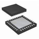
ICGOO电子元器件商城为您提供ADL5519ACPZ-R7由Analog设计生产,在icgoo商城现货销售,并且可以通过原厂、代理商等渠道进行代购。 ADL5519ACPZ-R7价格参考。AnalogADL5519ACPZ-R7封装/规格:RF 其它 IC 和模块, RF IC Detector/Controller WiMax, WLAN 1MHz ~ 10GHz 32-LFCSP-VQ (5x5)。您可以下载ADL5519ACPZ-R7参考资料、Datasheet数据手册功能说明书,资料中有ADL5519ACPZ-R7 详细功能的应用电路图电压和使用方法及教程。
ADL5519ACPZ-R7是Analog Devices Inc.推出的一款高性能射频(RF)对数检波器/控制器,属于RF其它IC和模块类别。该器件主要用于测量RF信号的功率电平,具备宽频带响应(可达10MHz至9GHz)和高动态范围(约65dB),适用于需要精确、快速RF功率检测的场景。

典型应用场景包括无线通信基础设施,如蜂窝基站中的发射功率控制与回波损耗监测;在RF自动增益控制(AGC)系统中,用于稳定输出信号强度,提升信号质量。此外,ADL5519ACPZ-R7也广泛应用于便携式与固定式无线设备中的功率管理,例如微波链路、雷达系统和测试测量仪器,能够实现对高频信号的实时监控与反馈调节。

其小尺寸、低功耗和高集成度特性,使其适合空间受限且对性能要求较高的应用环境。器件采用16引脚LFCSP封装,便于表面贴装,适合高密度PCB设计。总之,ADL5519ACPZ-R7是一款适用于多频段、高精度RF功率检测的关键元件,广泛服务于通信、工业和国防电子领域。
| 参数 | 数值 |
| 产品目录 | |
| 描述 | IC AMP LOG DETECT CTRLR 32LFCSP对数放大器 Dual Channel Log Detector |
| DevelopmentKit | ADL5519-EVALZ |
| 产品分类 | |
| 品牌 | Analog Devices |
| 产品手册 | |
| 产品图片 |
|
| rohs | 符合RoHS无铅 / 符合限制有害物质指令(RoHS)规范要求 |
| 产品系列 | 放大器 IC,对数放大器,Analog Devices ADL5519ACPZ-R7- |
| 数据手册 | |
| 产品型号 | ADL5519ACPZ-R7 |
| PCN组件/产地 | |
| RF类型 | WiMax,WLAN |
| 产品 | Logarithmic Amplifiers |
| 产品培训模块 | http://www.digikey.cn/PTM/IndividualPTM.page?site=cn&lang=zhs&ptm=25139 |
| 产品目录页面 | |
| 产品种类 | 对数放大器 |
| 供应商器件封装 | 32-LFCSP-VQ(5x5) |
| 其它名称 | ADL5519ACPZ-R7TR |
| 功能 | 检测器/控制器 |
| 包装 | 带卷 (TR) |
| 商标 | Analog Devices |
| 安装风格 | SMD/SMT |
| 封装 | Reel |
| 封装/外壳 | 32-VFQFN 裸露焊盘,CSP |
| 封装/箱体 | LFCSP-32 |
| 工作温度范围 | + 125 C |
| 工作电源电压 | 3.3 V to 5.5 V |
| 工厂包装数量 | 1500 |
| 带宽 | 10 GHz |
| 放大器类型 | Logarithmic |
| 最小工作温度 | - 40 C |
| 标准包装 | 1,500 |
| 电源电流 | 60 mA |
| 类型 | Log Amp Detector |
| 系列 | ADL5519 |
| 视频文件 | http://www.digikey.cn/classic/video.aspx?PlayerID=1364138032001&width=640&height=505&videoID=2245193150001 |
| 辅助属性 | - |
| 输入电压范围—最大 | 5.5 V |
| 通道数量 | 2 Channel |
| 频率 | 1MHz ~ 10GHz |


- 商务部:美国ITC正式对集成电路等产品启动337调查
- 曝三星4nm工艺存在良率问题 高通将骁龙8 Gen1或转产台积电
- 太阳诱电将投资9.5亿元在常州建新厂生产MLCC 预计2023年完工
- 英特尔发布欧洲新工厂建设计划 深化IDM 2.0 战略
- 台积电先进制程称霸业界 有大客户加持明年业绩稳了
- 达到5530亿美元!SIA预计今年全球半导体销售额将创下新高
- 英特尔拟将自动驾驶子公司Mobileye上市 估值或超500亿美元
- 三星加码芯片和SET,合并消费电子和移动部门,撤换高东真等 CEO
- 三星电子宣布重大人事变动 还合并消费电子和移动部门
- 海关总署:前11个月进口集成电路产品价值2.52万亿元 增长14.8%


PDF Datasheet 数据手册内容提取
1 MHz to 10 GHz, 62 dB Dual Log Detector/Controller Data Sheet ADL5519 FEATURES FUNCTIONAL BLOCK DIAGRAM Wide bandwidth: 1 MHz to 10 GHz OMR OMR PSA DJA PSR EMP LPA STA Dual-channel and channel difference output ports C C V A V T C V 24 23 22 21 20 19 18 17 Integrated accurate scaled temperature sensor 62 dB dynamic range (±3 dB) ADL5519 TEMP >50 dB with ±1 dB up to 8 GHz INHA 25 16 NC Stability over temperature: ±0.5 dB (−40oC to +85oC) INLA 26 CHANNEL A 15 OUTA Low noise detector/controller outputs LOG DETECTOR Pulse response time: 6 ns/8 ns (fall time/rise time) COMR 27 14 FBKA Supply operation: 3.3 V to 5.5 V @ 60 mA PWDN 28 13 OUTP OUTA Fabricated using high speed SiGe process OUTB COMR 29 12 OUTN Small footprint, 5 mm × 5 mm, 32-lead LFCSP Operating temperature range: −40oC to +125oC COMR 30 CHANNEL B 11 FBKB LOG DETECTOR APPLICATIONS INLB 31 10 OUTB INHB 32 9 NC RF transmitter power amplifier linearization and gain/power control BIAS Power monitoring in radio link transmitters 1 2 3 4 5 6 7 8 DAnutael-ncnhaa VnnSWel Rw mireolneistso irn frastructure radios COMR COMR VPSB ADJB VREF VLVL CLPB VSTB 06198-001 RSSI measurement in base stations, WLAN, WiMAX, radar Figure 1. GENERAL DESCRIPTION The ADL5519 is a dual-demodulating logarithmic amplifier that temperature conditions. A supply of 3.3 V to 5.5 V is required incorporates two AD8317s. It can accurately convert an RF input to power the device. Current consumption is typically 60 mA, signal into a corresponding decibel-scaled output. The ADL5519 and it decreases to less than 1 mA when the device is disabled. provides accurately scaled, independent, logarithmic output volt- The device is capable of supplying four log amp measurements ages for both RF measurement channels. The device has two simultaneously. Linear-in-dB measurements are provided at OUTA additional output ports, OUTP and OUTN, that provide the and OUTB with conveniently scaled slopes of −22 mV/dB. The log measured differences between the OUTA and OUTB channels. amp difference between OUTA and OUTB is available as differ- The on-chip channel matching makes the log amp outputs ential or single-ended signals at OUTP and OUTN. An optional insensitive to temperature and process variations. voltage applied to VLVL provides a common-mode reference level The temperature sensor pin provides a scaled voltage that is to offset OUTP and OUTN above ground. The broadband output proportional to the temperature over the operating temperature pins can support many system solutions. range of the device. Any of the ADL5519 output pins can be configured to provide The ADL5519 maintains accurate log conformance for signals a control voltage to a variable gain amplifier (VGA). Special from 1 MHz to 8 GHz and provides useful operation to 10 GHz. attention has been paid to minimize the broadband noise of the The ±3 dB dynamic range is typically 62 dB and has a ±1 dB output pins so that they can be used for controller applications. dynamic range of >50 dB (re: 50 Ω). The ADL5519 has a response The ADL5519 is fabricated on a SiGe bipolar IC process and is time of 6 ns/8 ns (fall time/rise time) that enables RF burst detec- available in a 5 mm × 5 mm, 32-lead LFCSP with an operating tion to a pulse rate of greater than 50 MHz. The device provides temperature range of −40°C to +125°C. unprecedented logarithmic intercept stability vs. ambient Rev. B Document Feedback Information furnished by Analog Devices is believed to be accurate and reliable. However, no responsibility is assumed by Analog Devices for its use, nor for any infringements of patents or other One Technology Way, P.O. Box 9106, Norwood, MA 02062-9106, U.S.A. rights of third parties that may result from its use. Specifications subject to change without notice. No license is granted by implication or otherwise under any patent or patent rights of Analog Devices. Tel: 781.329.4700 ©2008–2017 Analog Devices, Inc. All rights reserved. Trademarks and registered trademarks are the property of their respective owners. Technical Support www.analog.com
ADL5519 Data Sheet TABLE OF CONTENTS Features .............................................................................................. 1 Basis for Error Calculations ...................................................... 23 Applications ....................................................................................... 1 Device Calibration ..................................................................... 24 Functional Block Diagram .............................................................. 1 Adjusting Accuracy Through Choice of Calibration Points...... 24 General Description ......................................................................... 1 Temperature Compensation Adjustment................................ 25 Revision History ............................................................................... 2 Altering the Slope ....................................................................... 26 Specifications ..................................................................................... 3 Channel Isolation ....................................................................... 26 Absolute Maximum Ratings ............................................................ 9 Output Filtering .......................................................................... 27 ESD Caution .................................................................................. 9 Package Considerations ............................................................. 27 Pin Configuration and Function Descriptions ........................... 10 Operation Above 8 GHz ............................................................ 27 Typical Performance Characteristics ........................................... 11 Applications Information .............................................................. 28 Theory of Operation ...................................................................... 19 Measurement Mode ................................................................... 28 Using the ADL5519 ........................................................................ 20 Controller Mode ......................................................................... 28 Basic Connections ...................................................................... 20 Automatic Gain Control ............................................................ 30 Input Signal Coupling ................................................................ 20 Gain-Stable Transmitter/Receiver ............................................ 32 Temperature Sensor Interface ................................................... 22 Measuring VSWR ....................................................................... 34 VREF Interface ........................................................................... 22 Evaluation Board ............................................................................ 36 Power-Down Interface ............................................................... 22 Configuration Options .............................................................. 36 Setpoint Interface—VSTA, VSTB ............................................. 22 Evaluation Board Schematic and Artwork ............................. 37 Output Interface—OUTA, OUTB ............................................ 22 Outline Dimensions ....................................................................... 39 Difference Output—OUTP, OUTN ......................................... 23 Ordering Guide .......................................................................... 39 Description of Characterization ............................................... 23 REVISION HISTORY 9/2017—Rev. A to Rev. B 4/2009—Rev. 0 to Rev. A Changes to Figure 2 ........................................................................ 10 Changes to Table 5 .......................................................................... 36 Updated Outline Dimensions ....................................................... 39 Changes to Figure 72 ...................................................................... 37 Changes to Ordering Guide .......................................................... 39 1/2008—Revision 0: Initial Version Rev. B | Page 2 of 39
Data Sheet ADL5519 SPECIFICATIONS Supply voltage, V = VPSR = VPSA = VPSB = 5 V, C = 1000 pF, T = 25°C, 50 Ω termination resistor at INHA, INHB, unless otherwise noted. P LPF A Table 1. Parameter Conditions Min Typ Max Unit SIGNAL INPUT INTERFACE INHA, INHB (Pin 25, Pin 32) Specified Frequency Range 0.001 10 GHz DC Common-Mode Voltage V − 0.7 V P MEASUREMENT MODE, ADJA (Pin 21) = 0.65 V, ADJB (Pin 4) = 0.7 V; OUTA, OUTB 100 MHz OPERATION (Pin 15, Pin 10) shorted to VSTA, VSTB (Pin 17, Pin 8); OUTP, OUTN (Pin 13, Pin 12) shorted to FBKA, FBKB (Pin 14, Pin 11), respectively; sinusoidal input signal; error referred to best-fit line using linear regression between P , P = −40 dBm and −10 dBm INHA INHB Input Impedance 1670||0.47 Ω||pF OUTA, OUTB ± 1 dB Dynamic Range 51 dB −40°C < T < +85°C 42 dB A OUTA, OUTB Maximum Input Level ±1 dB error −1 dBm OUTA, OUTB Minimum Input Level ±1 dB error −52 dBm OUTA, OUTB, OUTP, OUTN Slope1 −22 mV/dB OUTA, OUTB Intercept1 22 dBm Output Voltage (High Power In) OUTA, OUTB @ P , P = −16 dBm 0.7 V INHA INHB Output Voltage (Low Power In) OUTA, OUTB @ P , P = −40 dBm 1.37 V INHA INHB OUTP, OUTN Dynamic Gain Range ±1 dB error 50 dB −40°C < T < +85°C 44 dB A Temperature Sensitivity Deviation from OUTA, OUTB @ 25°C −40°C < T < +85°C, P , P = −16 dBm ±0.25 dB A INHA INHB 25°C < T < 85°C, P , P = −40 dBm +0.16 dB A INHA INHB −40°C < T < +25°C, P , P = −40 dBm −0.6 dB A INHA INHB Distribution of OUTP, OUTN from 25°C 25°C < T < 85°C, P = −16 dBm, P = −30 dBm, ±0.25 dB A INHA INHB typical error = −0.09 dB −40°C < T < +25°C, P = −16 dBm, P = −30 dBm, ±0.4 dB A INHA INHB typical error = 0.25 dB 25°C < T < 85°C, P = −40 dBm, P = −30 dBm, ±0.25 dB A INHA INHB typical error = 0.05 dB −40°C < T < +25°C, P = −40 dBm, P = −30 dBm, ±0.45 dB A INHA INHB typical error = −0.23 dB Input A-to-Input B Isolation 80 dB Input A-to-OUTB Isolation Frequency separation = 1 kHz, P = −50 dBm, 60 dB INHA P – P when OUTB/Slope = 1 dB INHA INHB Input B-to-OUTA Isolation Frequency separation = 1 kHz, P = −50 dBm, 60 dB INHB P – P when OUTA/Slope = 1 dB INHB INHA MEASUREMENT MODE, ADJA = 0.6 V, ADJB = 0.65 V; OUTA, OUTB shorted to 900 MHz OPERATION VSTA, VSTB; OUTP, OUTN shorted to FBKA, FBKB, respectively; sinusoidal input signal; error referred to best fit line using linear regression between P , P = −40 dBm and −10 dBm INHA INHB Input Impedance 925||0.54 Ω||pF OUTA, OUTB ± 1 dB Dynamic Range 54 dB −40°C < T < +85°C 49 dB A OUTA, OUTB Maximum Input Level ±1 dB error −2 dBm OUTA, OUTB Minimum Input Level ±1 dB error −56 dBm OUTA, OUTB, OUTP, OUTN Slope1 −22 mV/dB OUTA, OUTB Intercept1 20.3 dBm Output Voltage (High Power In) OUTA, OUTB @ P , P = −10 dBm 0.67 V INHA INHB Output Voltage (Low Power In) OUTA, OUTB @ P , P = −40 dBm 1.34 V INHA INHB Rev. B | Page 3 of 39
ADL5519 Data Sheet Parameter Conditions Min Typ Max Unit OUTP, OUTN Dynamic Gain Range ±1 dB error 55 dB −40°C < T < +85°C 48 dB A Temperature Sensitivity Deviation from OUTA, OUTB @ 25°C −40°C < T < +85°C, P , P = −16 dBm ±0.25 dB A INHA INHB 25°C < T < 85°C, P , P = −40 dBm +0.25 dB A INHA INHB −40°C < T < +25°C, P , P = −40 dBm −0.5 dB A INHA INHB Distribution OUTP, OUTN from 25°C 25°C < T < 85°C, P = −16 dBm, P = −30 dBm, ±0.25 dB A INHA INHB typical error = −0.08 dB −40°C < T < +25°C, P = −16 dBm, P = −30 dBm ±0.4 dB A INHA INHB typical error = 0.3 dB 25°C < T < 85°C, P = −40 dBm, P = −30 dBm, ±0.25 dB A INHA INHB typical error = 0.17 dB −40°C < T < +25°C, P = −40 dBm, P = −30 dBm, ±0.4 dB A INHA INHB typical error = −0.19 dB Input A-to-Input B Isolation 75 dB Input A-to-OUTB Isolation Frequency separation = 1 kHz, P = −50 dBm, 50 dB INHA P – P when OUTB/Slope = 1 dB INHA INHB Input B-to-OUTA Isolation Frequency separation = 1 kHz, P = −50 dBm, 50 dB INHB P – P when OUTA/Slope = 1 dB INHB INHA MEASUREMENT MODE, ADJA = 0.5 V, ADJB = 0.55 V; OUTA, OUTB shorted to 1.9 GHz OPERATION VSTA, VSTB; OUTP, OUTN shorted to FBKA, FBKB, respectively; sinusoidal input signal; error referred to best fit line using linear regression between P , P = −40 dBm and −10 dBm INHA INHB Input Impedance 525||0.36 Ω||pF OUTA, OUTB ± 1 dB Dynamic Range 55 dB −40°C < T < +85°C 49 dB A OUTA, OUTB Maximum Input Level ±1 dB error −4 dBm OUTA, OUTB Minimum Input Level ±1 dB error −59 dBm OUTA, OUTB, OUTP, OUTN Slope1 −22 mV/dB OUTA, OUTB Intercept1 18 dBm Output Voltage (High Power In) OUTA, OUTB @ P , P = −10 dBm 0.62 V INHA INHB Output Voltage (Low Power In) OUTA, OUTB @ P , P = −40 dBm 1.28 V INHA INHB OUTP, OUTN Dynamic Gain Range ±1 dB error 55 dB −40°C < T < +85°C 48 dB A Temperature Sensitivity Deviation from OUTA, OUTB @ 25°C −40°C < T < +85°C, P , P = −16 dBm ±0.2 dB A INHA INHB 25°C < T < 85°C, P , P = −40 dBm +0.25 dB A INHA INHB −40°C < T < +25°C, P , P = −40 dBm −0.5 dB A INHA INHB Distribution of OUTP, OUTN from 25°C 25°C < T < 85°C, P = −16 dBm, P = −30 dBm, ±0.3 dB A INHA INHB typical error = −0.07 dB −40°C < T < +25°C, P = −16 dBm, P = −30 dBm, ±0.4 dB A INHA INHB typical error = 0.23 dB 25°C < T < 85°C, P = −40 dBm, P = −30 dBm, ±0.3 dB A INHA INHB typical error = 0.16 dB −40°C < T < +25°C, P = −40 dBm, P = −30 dBm, ±0.4 dB A INHA INHB typical error = −0.22 dB Input A-to-Input B Isolation 65 dB Input A-to-OUTB Isolation Frequency separation = 1 kHz, P = −50 dBm, 46 dB INHA P – P when OUTB/Slope = 1 dB INHA INHB Input B-to-OUTA Isolation Frequency separation = 1 kHz, P = −50 dBm, 46 dB INHB P – P when OUTA/Slope = 1 dB INHB INHA Rev. B | Page 4 of 39
Data Sheet ADL5519 Parameter Conditions Min Typ Max Unit MEASUREMENT MODE, ADJA = 0.48 V, ADJB = 0.6 V; OUTA, OUTB shorted to 2.2 GHz OPERATION VSTA, VSTB; OUTP, OUTN shorted to FBKA, FBKB, respectively; sinusoidal input signal; error referred to best fit line using linear regression between P , P = −40 dBm and −10 dBm INHA INHB Input Impedance 408||0.34 Ω||pF OUTA, OUTB ± 1 dB Dynamic Range 55 dB −40°C < T < +85°C 50 dB A OUTA, OUTB Maximum Input Level ±1 dB error −5 dBm OUTA, OUTB Minimum Input Level ±1 dB error −60 dBm OUTA, OUTB, OUTP, OUTN Slope1 −22 mV/dB OUTA, OUTB Intercept1 16.9 dBm Output Voltage (High Power In) OUTA, OUTB @ P , P = −10 dBm 0.6 V INHA INHB Output Voltage (Low Power In) OUTA, OUTB @ P , P = −40 dBm 1.26 V INHA INHB OUTP, OUTN Dynamic Gain Range ±1 dB error 56 dB −40°C < T < +85°C 40 dB A Temperature Sensitivity Deviation from OUTA, OUTB @ 25°C −40°C < T < +85°C, P , P = −16 dBm ±0.28 dB A INHA INHB 25°C < T < 85°C, P , P = −40 dBm +0.3 dB A INHA INHB −40°C < T < +25°C, P , P = −40 dBm −0.5 dB A INHA INHB Distribution of OUTP, OUTN from 25°C 25°C < T < 85°C, P = −16 dBm, P = −30 dBm, ±0.25 dB A INHA INHB typical error = −0.07 dB −40°C < T < +25°C, P = −16 dBm, P = −30 dBm, ±0.4 dB A INHA INHB typical error = 0.25 dB 25°C < T < 85°C, P = −40 dBm, P = −30 dBm, ±0.25 dB A INHA INHB typical error = 0.17 dB −40°C < T < +25°C, P = −40 dBm, P = −30 dBm ±0.4 dB A INHA INHB typical error = −0.22dB Input A-to-Input B Isolation 60 dB Input A-to-OUTB Isolation Frequency separation = 1 kHz, P = −50 dBm, 46 dB INHA P – P when OUTB/Slope = 1 dB INHA INHB Input B-to-OUTA Isolation Frequency separation = 1 kHz, P = −50 dBm, 46 dB INHB P – P when OUTA/Slope = 1 dB INHB INHA MEASUREMENT MODE, ADJA = 0.35 V ADJB = 0.42; OUTA, OUTB shorted to 3.6 GHz OPERATION VSTA, VSTB; OUTP, OUTN shorted to FBKA, FBKB, respectively; sinusoidal input signal; error referred to best fit line using linear regression between P , P = −40 dBm and −10 dBm INHA INHB Input Impedance 187||0.66 Ω||pF OUTA, OUTB ± 1 dB Dynamic Range 54 dB −40°C < T < +85°C 44 dB A OUTA, OUTB Maximum Input Level ±1 dB error −4 dBm OUTA, OUTB Minimum Input Level ±1 dB error −58 dBm OUTA, OUTB, OUTP, OUTN Slope1 −22.5 mV/dB OUTA, OUTB Intercept1 17 dBm Output Voltage (High Power In) OUTA, OUTB @ P , P = −10 dBm 0.62 V INHA INHB Output Voltage (Low Power In) OUTA, OUTB @ P , P = −40 dBm 1.31 V INHA INHB OUTP, OUTN Dynamic Gain Range ±1 dB error 52 dB −40°C < T < +85°C 42 dB A Rev. B | Page 5 of 39
ADL5519 Data Sheet Parameter Conditions Min Typ Max Unit Temperature Sensitivity Deviation from OUTA, OUTB @ 25°C −40°C < T < +85°C, P , P = −16 dBm ±0.4 dB A INHA INHB 25°C < T < 85°C, P , P = −40 dBm +0.6 dB A INHA INHB −40°C < T < +25°C, P , P = −40 dBm −0.45 dB A INHA INHB Distribution of OUTP, OUTN from 25°C 25°C < T < 85°C, P = −16 dBm, P = −30 dBm, ±0.25 dB A INHA INHB typical error = −0.07 dB −40°C < T < +25°C, P = −16 dBm, P = −30 dBm, ±0.45 dB A INHA INHB typical error = 0.27 dB 25°C < T < 85°C, P = −40 dBm, P = −30 dBm, ±0.3 dB A INHA INHB typical error = 0.31 dB −40°C < T < +25°C, P = −40 dBm, P = −30 dBm, ±0.5 dB A INHA INHB typical error = −0.14 dB Input A-to-Input B Isolation 40 dB Input A-to-OUTB Isolation Frequency separation = 1 kHz, P = −50 dBm, 20 dB INHA P – P when OUTB/Slope = 1 dB INHA INHB Input B-to-OUTA Isolation Frequency separation = 1 kHz, P = −50 dBm, 20 dB INHB P – P when OUTA/Slope = 1 dB INHB INHA MEASUREMENT MODE, ADJA = 0.58 V, ADJB = 0.7 V; OUTA, OUTB shorted to 5.8 GHz OPERATION VSTA, VSTB; OUTP, OUTN shorted to FBKA, FBKB respectively; sinusoidal input signal; error referred to best fit line using linear regression between P , P = −40 dBm and −20 dBm INHA INHB Input Impedance 28||1.19 Ω||pF OUTA, OUTB ± 1 dB Dynamic Range 53 dB −40°C < T < +85°C 45 dB A OUTA, OUTB Maximum Input Level ±1 dB error −2 dBm OUTA, OUTB Minimum Input Level ±1 dB error −55 dBm OUTA, OUTB, OUTP, OUTN Slope1 −22.5 mV/dB OUTA, OUTB Intercept1 20 dBm Output Voltage (High Power In) OUTA, OUTB @ P , P = −10 dBm 0.68 V INHA INHB Output Voltage (Low Power In) OUTA, OUTB @ P , P = −40 dBm 1.37 V INHA INHB OUTP, OUTN Dynamic Gain Range ±1 dB error 53 dB −40°C < T < +85°C 46 dB A Temperature Sensitivity Deviation from OUTA, OUTB @ 25°C −40°C < T < +85°C, P , P = −16dBm ±0.25 dB A INHA INHB 25°C < T < 85°C, P , P = −40 dBm +0.25 dB A INHA INHB −40°C < T < +25°C, P , P = −40 dBm −0.4 dB A INHA INHB Distribution of OUTP, OUTN from 25°C 25°C < T < 85°C, P = −16 dBm, P = −30 dBm, ±0.3 dB A INHA INHB typical error = 0.02 dB −40°C < T < +25°C, P = −16 dBm, P = −30 dBm, ±0.4 dB A INHA INHB typical error = 0.25 dB 25°C < T < 85°C, P = −40 dBm, P = −30 dBm, ±0.3 dB A INHA INHB typical error = 0.13 dB −40°C < T < +25°C, P = −40 dBm, P = −30 dBm, ±0.5 dB A INHA INHB typical error = 0.06 dB Input A-to-Input B Isolation 45 dB Input A-to-OUTB Isolation Frequency separation = 1 kHz, P = −50 dBm, 48 dB INHA P – P when OUTB/Slope = 1 dB INHA INHB Input B-to-OUTA Isolation Frequency separation = 1 kHz, P = −50 dBm, 48 dB INHB P – P when OUTA/Slope = 1 dB INHB INHA Rev. B | Page 6 of 39
Data Sheet ADL5519 Parameter Conditions Min Typ Max Unit MEASUREMENT MODE, ADJA = 0.72 V, ADJB = 0.82 V to GND; OUTA, OUTB shorted 8 GHz OPERATION to VSTA, VSTB; OUTP, OUTN shorted to FBKA, FBKB, respectively; sinusoidal input signal; error referred to best fit line using linear regression between P , P = −40 dBm and −20 dBm INHA INHB Input Impedance +10||−1.92 Ω||pF OUTA, OUTB ± 1 dB Dynamic Range 48 dB −40°C < T < +85°C 38 dB A OUTA, OUTB Maximum Input Level ±1 dB error 0 dBm OUTA, OUTB Minimum Input Level ±1 dB error −48 dBm OUTA, OUTB, OUTP, OUTN Slope1 −22 mV/dB OUTA, OUTB Intercept1 26 dBm Output Voltage (High Power In) OUTA, OUTB @ P , P = −10 dBm 0.81 V INHA INHB Output Voltage (Low Power In) OUTA, OUTB @ P , P = −40 dBm 1.48 V INHA INHB OUTP, OUTN Dynamic Gain Range ±1 dB error 50 dB −40°C < T < +85°C 42 dB A Temperature Sensitivity Deviation from OUTA, OUTB @ 25°C −40°C < T < +85°C, P , P = −16 dBm ±0.4 dB A INHA INHB 25°C < T < 85°C, P , P = −40 dBm −0.1 dB A INHA INHB −40°C < T < +25°C, P , P = −40 dBm +0.5 dB A INHA INHB Distribution of OUTP, OUTN from 25°C 25°C < T < 85°C, P = −16 dBm, P = −30 dBm, ±0.3 dB A INHA INHB typical error = 0.2dB −40°C < T < +25°C, P = −16 dBm, P = −30 dBm, ±0.5 dB A INHA INHB typical error = 0.09dB 25°C < T < 85°C, P = −40 dBm, P = −30 dBm, ±0.3 dB A INHA INHB typical error = −0.07dB −40°C < T < +25°C, P = −40 dBm, P = −30 dBm, ±0.5 dB A INHA INHB typical error = 0.17 dB Input A-to-Input B Isolation 45 dB Input A-to-OUTB Isolation Frequency separation = 1 kHz, P = −50 dBm, 30 dB INHA P – P when OUTB/Slope = 1 dB INHA INHB Input B-to-OUTA Isolation Frequency separation = 1 kHz, P = −50 dBm, 30 dB INHB P – P when OUTA/Slope = 1 dB INHB INHA OUTPUT INTERFACE OUTA, OUTB; OUTP, OUTN OUTA, OUTB Voltage Range VSTA, VSTB = 1.7 V, RF in = open 0.3 V VSTA, VSTB = 0 V, RF in = open V − 0.4 V P OUTP, OUTN Voltage Range FBKA, FBKB = open and OUTA < OUTB, R ≥ 240 Ω to ground 0.09 V L FBKA, FBKB = open and OUTA > OUTB, R ≥ 240 Ω to ground V − 0.15 V L P Source/Sink Current Output held at 1 V to 1% change 10 mA Capacitance Drive 1 nF Output Noise INHA, INHB = 2.2 GHz, −10 dBm, f = 100 kHz, 10 nV/√Hz NOISE CLPA, CLPB = open Fall Time Input level = no signal to −10 dBm, 80% to 20%, 12 ns CLPA, CLPB = 10 pF Input level = no signal to −10 dBm, 80% to 20%, 6 ns CLPA, CLPB = open Rise Time Input level = −10 dBm to no signal, 20% to 80%, 16 ns CLPA, CLPB = 10 pF Input level = −10 dBm to no signal, 20% to 80%, 8 ns CLPA, CLPB = open Video Bandwidth 10 MHz (or Envelope Bandwidth) SETPOINT INTERFACE VSTA, VSTB Nominal Input Range Input level = 0 dBm, measurement mode 0.38 V Input level = –50 dBm, measurement mode 1.6 V Input Resistance Controller mode, sourcing 50 µA 40 kΩ Rev. B | Page 7 of 39
ADL5519 Data Sheet Parameter Conditions Min Typ Max Unit DIFFERENCE LEVEL ADJUST VLVL (Pin 6) Input Voltage OUTP, OUTN = FBKA, FBKB V − 1 V P Input Resistance OUTP, OUTN = FBKA, FBKB 100 kΩ TEMPERATURE COMPENSATION ADJA, ADJB Input Resistance ADJA, ADJB = 0.9 V, sourcing 50 µA 13 kΩ Disable Threshold Voltage ADJA, ADJB = open V − 0.4 V P VOLTAGE REFERENCE VREF (Pin 5) Output Voltage 1.15 V Temperature Sensitivity −40°C < T < +25°C; relative T = 25°C +26 µV/°C A A 25°C < T < 85°C; relative T = 25°C −26 µV/°C A A Current Limit Source/Sink 3/3 mA TEMPERATURE REFERENCE TEMP (Pin 19) Output Voltage 1.36 V Temperature Sensitivity −40°C < T < +125°C 4.5 mV/°C A Current Limit Source/Sink 4/50 mA/µA POWER-DOWN INTERFACE PWDN (Pin 28) Logic Level to Enable Logic low enables 0 V Logic Level to Disable Logic high disables V − 0.2 V P Input Current Logic high PWDN = 5 V 2 µA Logic low PWDN = 0 V 20 µA Enable Time PWDN low to OUTA, OUTB at 100% final value, 0.4 µs CLPA, CLPB = open, RF in = −10 dBm Disable Time PWDN high to OUTA, OUTB at 10% final value, 0.25 µs CLPA, CLPB = open, RF in = 0 dBm POWER INTERFACE VPSA, VPSB, VPSR Supply Voltage 3.3 5.5 V Quiescent Current 60 mA vs. Temperature −40°C ≤ T ≤ +85°C 147 µA/°C A Disable Current ADJA, ADJB = PWDN = V <1 mA P 1 Slope and intercept are determined by calculating the best-fit line between the power levels of −40 dBm and −10 dBm at the specified input frequency. Rev. B | Page 8 of 39
Data Sheet ADL5519 ABSOLUTE MAXIMUM RATINGS Stresses at or above those listed under Absolute Maximum Table 2. Ratings may cause permanent damage to the product. This is a Parameter Rating stress rating only; functional operation of the product at these Supply Voltage: VPSA, VPSB, VPSR 5.7 V or any other conditions above those indicated in the operational V Voltage: VSTA, VSTB 0 to V SET P section of this specification is not implied. Operation beyond Input Power (Single-Ended, Re: 50 Ω) 12 dBm INHA, INLA, INHB, INLB the maximum operating conditions for extended periods may Internal Power Dissipation 420 mW affect product reliability. θ 42°C/W JA Maximum Junction Temperature 142°C ESD CAUTION Operating Temperature Range −40°C to +125°C Storage Temperature Range −65°C to +150°C Lead Temperature (Soldering, 60 sec) 260°C Rev. B | Page 9 of 39
ADL5519 Data Sheet PIN CONFIGURATION AND FUNCTION DESCRIPTIONS RRNR BBMMDMAA HNILNIOCOCWPOCLNIHNI 21098765 33322222 COMR 1 24 COMR COMR 2 23 COMR VPSB 3 22 VPSA ADJB 4 ADL5519 21 ADJA VREF 5 TOP VIEW 20 VPSR VLVL 6 (Not to Scale) 19 TEMP CLPB 7 18 CLPA VSTB 8 17 VSTA 910111213141516 CBBNPAAC NTKTTKTN UBUUBU OFOOFO NOTES 12.. ENCXCOP N=ON NSEOEC DTCEOPDANDNT OEMC UCTSO.TM BRE. INTERNALLY 06198-002 Figure 2. Pin Configuration Table 3. Pin Function Descriptions Pin No. Mnemonic Description 1 COMR Connect via low impedance to common. 2 COMR Connect via low impedance to common. 3 VPSB Positive Supply for Channel B. Apply 3.3 V to 5.5 V supply voltage. 4 ADJB Dual-Function Pin: Temperature Adjust Pin for Channel B and Power-Down Interface for OUTB. 5 VREF Voltage Reference (1.15 V). 6 VLVL DC Common-Mode Adjust for Difference Output. 7 CLPB Loop Filter Pin for Channel B. 8 VSTB Setpoint Control Input for Channel B. 9 NC No Connect. 10 OUTB Output Voltage for Channel B. 11 FBKB Difference Op Amp Feedback Pin for OUTN Op Amp. 12 OUTN Difference Output (OUTB − OUTA + VLVL). 13 OUTP Difference Output (OUTA − OUTB + VLVL). 14 FBKA Difference Op Amp Feedback Pin for OUTP Op Amp. 15 OUTA Output Voltage for Channel A. 16 NC No Connect. 17 VSTA Setpoint Control Input for Channel A. 18 CLPA Loop Filter Pin for Channel A. 19 TEMP Temperature Sensor Output (1.3 V with 4.5 mV/°C Slope). 20 VPSR Positive Supply for Difference Outputs and Temperature Sensor. Apply 3.3 V to 5.5 V supply voltage. 21 ADJA Dual-Function Pin: Temperature Adjust Pin for Channel A and Power-Down Interface for OUTA. 22 VPSA Positive Supply for Channel A. Apply 3.3 V to 5.5 V supply voltage. 23 COMR Connect via low impedance to common. 24 COMR Connect via low impedance to common. 25 INHA AC-Coupled RF Input for Channel A. 26 INLA AC-Coupled RF Common for Channel A. 27 COMR Connect via low impedance to common. 28 PWDN Power-Down for Difference Output and Temperature Sensor. 29 COMR Connect via low impedance to common. 30 COMR Connect via low impedance to common. 31 INLB AC-Coupled RF Common for Channel B. 32 INHB AC-Coupled RF Input for Channel B. Paddle Internally connected to COMR. Rev. B | Page 10 of 39
Data Sheet ADL5519 TYPICAL PERFORMANCE CHARACTERISTICS V = 5 V; T = +25°C, −40°C, +85°C; CLPA, CLPB = 1 µF. Colors: +25°C black, −40°C blue, +85°C red. P A 2.00 2.0 2.0 2.0 1.75 1.5 E (V) OUTP OUTN E (V) 1.50 1.0 OLTAG 1.5 N 1.0 UTPUT VOLTAG 110...207505 00–.05.5 ERROR (dB) UTN OUTPUT V 1.0 P 0 ERROR (dB) O O 0.50 –1.0 P, 0.5 –1.0 T U O 0.25 –1.5 0 –2.0 0 –2.0 –60 –50 –40 –3P0IN (dBm–2)0 –10 0 10 06198-003 –60 –50 –40 –3P0IN (dBm–2)0 –10 0 10 06198-006 Figure 3. OUTA, OUTB Voltage and Log Conformance vs. Input Amplitude Figure 6. OUTP, OUTN Gain Error and Voltage vs. Input Amplitude at 100 MHz, at 100 MHz, Typical Device, ADJA, ADJB = 0.65 V, 0.7 V, Sine Wave, Typical Device, ADJA, ADJB = 0.65 V, 0.7, Sine Wave, Single-Ended Drive, Single-Ended Drive PINHB = −30 dBm, Channel A Swept 2.0 1.5 2.0 1.5 V) 1.0 E ( G 1.0 A 1.0 T 0.5 L O ERROR (dB) –00..550 TN OUTPUT V –0.50 0 ERROR (dB) U O –1.0 P – –1.0 –1.0 T U –1.5 O –1.5 –2.0 –2.0 –2.0 –60 –50 –40 –3P0IN (dBm–2)0 –10 0 10 06198-004 –60 –50 –40 –3P0IN (dBm–2)0 –10 0 10 06198-007 Figure 4. Distribution of OUTA, OUTB Error over Temperature After Ambient Figure 7. Distribution of [OUTP − OUTN] Gain Error and Voltage vs. Input Normalization vs. Input Amplitude for 45 Devices, Frequency = 100 MHz, Amplitude over Temperature, After Ambient Normalization for 45 Devices from ADJA, ADJB = 0.65 V, 0.7 V, Sine Wave, Single-Ended Drive a Nominal Lot, Frequency = 100 MHz, ADJA, ADJB = 0.65 V, 0.7 V, Sine Wave, Single-Ended Drive, PINHB = −30 dBm, Channel A Swept 2.0 2.00 2.0 1.5 1.75 1.5 1.0 1.50 1.0 V) V) E ( UTA – OUTB ( –00..550 PUT VOLTAG 110...207505 00–.05.5 ERROR (dB) O T U O –1.0 0.50 –1.0 –1.5 0.25 –1.5 –2.0 0 –2.0 –60 –50 –40 –3P0IN (dBm–2)0 –10 0 10 06198-005 –60 –50 –40 –3P0IN (dBm–2)0 –10 0 10 06198-008 Figure 5. Distribution of [OUTA − OUTB] Voltage Difference over Temperature Figure 8. OUTA, OUTB Voltage and Log Conformance vs. Input Amplitude for 45 Devices from a Nominal Lot, Frequency = 100 MHz, at 900 MHz, Typical Device, ADJA, ADJB = 0.6 V, 0.65 V, Sine Wave, ADJA, ADJB = 0.65 V, 0.7 V, Sine Wave, Single-Ended Drive Single-Ended Drive Rev. B | Page 11 of 39
ADL5519 Data Sheet 2.0 2.0 2.0 V) 1.5 E ( G 1.0 A 1.0 1.0 T L O ERROR (dB) 0 TN OUTPUT V –00..550 0 ERROR (dB) U O –1.0 P – –1.0 –1.0 T U O –1.5 –2.0 –2.0 –2.0 –60 –50 –40 –3P0IN (dBm–2)0 –10 0 10 06198-009 –60 –50 –40 –3P0IN (dBm–2)0 –10 0 10 06198-012 Figure 9. Distribution of OUTA, OUTB Error over Temperature After Ambient Figure 12. Distribution of [OUTP − OUTN] Gain Error and Voltage vs. Input Normalization vs. Input Amplitude for 45 Devices, Frequency = 900 MHz, Amplitude over Temperature, After Ambient Normalization for 45 Devices ADJA, ADJB = 0.6 V, 0.65 V, Sine Wave, Single-Ended Drive from a Nominal Lot, Frequency = 900 MHz, ADJA, ADJB = 0.6 V, 0.65 V, Sine Wave, Single-Ended Drive, PINHB = −30 dBm, Channel A Swept 0.20 2.0 2.0 0.15 0.10 1.5 1.0 V) V) E ( B ( 0.05 AG B) UTA – OUT–0.050 PUT VOLT 1.0 0 ERROR (d O UT O –0.10 0.5 –1.0 –0.15 –0.20 0 –2.0 –60 –50 –40 –3P0IN (dBm–2)0 –10 0 10 06198-010 –60 –50 –40 –3P0IN (dBm–2)0 –10 0 10 06198-013 Figure 10. Distribution of [OUTA − OUTB] Voltage Difference over Figure 13. OUTA, OUTB Voltage and Log Conformance vs. Input Amplitude at Temperature for 45 Devices from a Nominal Lot, Frequency = 900 MHz, 1.9 GHz, Typical Device, ADJA, ADJB = 0.5 V, 0.55 V, Sine Wave, ADJA, ADJB = 0.6 V, 0.65 V, Sine Wave, Single-Ended Drive Single-Ended Drive 2.0 2.0 2.0 V) E ( OUTP OUTN AG 1.5 1.0 1.0 T OL N TPUT V 1.0 0 OR (dB) OR (dB) 0 U R R N O P ER ER T U O P, 0.5 –1.0 –1.0 T U O 0 –2.0 –2.0 –60 –50 –40 –3P0IN (dBm–2)0 –10 0 10 06198-011 –60 –50 –40 –3P0IN (dBm–2)0 –10 0 10 06198-014 Figure 11. OUTP, OUTN Gain Error and Voltage vs. Input Amplitude at Figure 14. Distribution of OUTA, OUTB Error over Temperature After Ambient 900 MHz, Typical Device, ADJA, ADJB = 0.6 V, 0.65 V, Sine Wave, Normalization vs. Input Amplitude for 45 Devices, Frequency = 1.9 GHz, Single-Ended Drive; PINHB = −30 dBm, Channel A Swept ADJA, ADJB = 0.5 V, 0.55 V, Sine Wave, Single-Ended Drive Rev. B | Page 12 of 39
Data Sheet ADL5519 0.20 2.0 2.0 0.15 0.10 1.5 1.0 V) V) E ( B ( 0.05 AG B) UTA – OUT–0.050 PUT VOLT 1.0 0 ERROR (d O UT O –0.10 0.5 –1.0 –0.15 –0.20 0 –2.0 –60 –50 –40 –3P0IN (dBm–2)0 –10 0 10 06198-015 –60 –50 –40 –3P0IN (dBm–2)0 –10 0 10 06198-018 Figure 15. Distribution of [OUTA – OUTB] Voltage Difference over Figure 18. OUTA, OUTB Voltage and Log Conformance vs. Input Amplitude at Temperature for 45 Devices from a Nominal Lot, Frequency = 1.9 GHz, 2.2 GHz, Typical Device, ADJA, ADJB = 0.48 V, 0.6 V, Sine Wave, ADJA, ADJB = 0.5 V, 0.55 V, Sine Wave, Single-Ended Drive Single-Ended Drive 2.0 2.0 2.0 V) E ( OUTP OUTN AG 1.5 1.0 1.0 T OL N TPUT V 1.0 0 OR (dB) OR (dB) 0 U R R O R R N P E E T U O P, 0.5 –1.0 –1.0 T U O 0 –2.0 –2.0 –60 –50 –40 –3P0IN (dBm–2)0 –10 0 10 06198-016 –60 –50 –40 –3P0IN (dBm–2)0 –10 0 10 06198-019 Figure 16. OUTP, OUTN Gain Error and Voltage vs. Input Amplitude at Figure 19. Distribution of OUTA, OUTB Error over Temperature After Ambient 1.9 GHz, with B Input Held at −30 dBm and A Input Swept, Typical Device, Normalization vs. Input Amplitude for at Least 45 Devices from a Nominal Lot, ADJA, ADJB = 0.5 V, 0.55 V, Sine Wave, Single-Ended Drive, Frequency = 2.2 GHz, ADJA, ADJB = 0.48 V, 0.6 V, Sine Wave, Single-Ended Drive PINHB = −30 dBm, Channel A Swept 2.0 2.0 0.20 V) 1.5 0.15 E ( G A 1.0 0.10 T 1.0 OL V) TN OUTPUT V 0.50 0 ERROR (dB) UTA – OUTB (–00..00550 U O O P – –0.5 –1.0 –0.10 T U O –1.0 –0.15 –1.5 –2.0 –0.20 –60 –50 –40 –3P0IN (dBm–2)0 –10 0 10 06198-017 –60 –50 –40 –3P0IN (dBm–2)0 –10 0 10 06198-020 Figure 17. Distribution of [OUTP − OUTN] Gain Error and Voltage vs. Input Figure 20. Distribution of [OUTA – OUTB] Voltage Difference over Amplitude over Temperature, After Ambient Normalization for 45 Devices Temperature for 45 Devices from a Nominal Lot, Frequency = 2.2 GHz, from a Nominal Lot, Frequency = 1.9 GHz, ADJA, ADJB = 0.5 V, 0.55 V, ADJA, ADJB = 0.48 V, 0.6 V, Sine Wave, Single-Ended Drive Sine Wave, Single-Ended Drive, PINHB = −30 dBm, Channel A Swept Rev. B | Page 13 of 39
ADL5519 Data Sheet 2.0 2.0 2.0 V) E ( OUTP OUTN AG 1.5 1.0 1.0 T L N O TPUT V 1.0 0 OR (dB) OR (dB) 0 U R R N O P ER ER T U O P, 0.5 –1.0 –1.0 T U O 0 –2.0 –2.0 –60 –50 –40 –3P0IN (dBm–2)0 –10 0 10 06198-021 –60 –50 –40 –3P0IN (dBm–2)0 –10 0 10 06198-024 Figure 21. OUTP, OUTN Gain Error and Voltage vs. Input Amplitude at 2.2 GHz, Figure 24. Distribution of OUTA, OUTB Error over Temperature After Ambient Typical Device, ADJA, ADJB = 0.48 V, 0.6 V, Sine Wave, Single-Ended Drive, Normalization vs. Input Amplitude for 45 Devices from a Nominal Lot, PINHB = −30 dBm, Channel A Swept Frequency = 3.6 GHz, ADJA, ADJB = 0.35 V, 0.42 V, Sine Wave, Single-Ended Drive 2.0 2.0 0.20 V) 1.5 0.15 E ( G A 1.0 0.10 T 1.0 OL V) UTN OUTPUT V 0.50 0 ERROR (dB) OUTA – OUTB (–00..00550 O P – –0.5 –1.0 –0.10 T U O –1.0 –0.15 –1.5 –2.0 –0.20 –60 –50 –40 –3P0IN (dBm–2)0 –10 0 10 06198-022 –60 –50 –40 –3P0IN (dBm–2)0 –10 0 10 06198-025 Figure 22. Distribution of [OUTP − OUTN] Gain Error and Voltage vs. Input Figure 25. Distribution of [OUTA – OUTB] Voltage Difference over Amplitude over Temperature, After Ambient Normalization for 45 Devices Temperature for 45 Devices from a Nominal Lot, Frequency = 3.6 GHz, from a Nominal Lot, Frequency = 2.2 GHz, ADJA, ADJB = 0.48 V, 0.6 V, ADJA, ADJB = 0.35 V, 0.42 V, Sine Wave, Single-Ended Drive Sine Wave, Single-Ended Drive, PINHB = −30 dBm, Channel A Swept 2.0 2.0 2.0 2.0 V) E ( OUTP OUTN E (V) 1.5 1.0 OLTAG 1.5 N 1.0 PUT VOLTAG 1.0 0 ERROR (dB) N OUTPUT V 1.0 P 0 ERROR (dB) UT UT O O 0.5 –1.0 P, 0.5 –1.0 T U O 0 –2.0 0 –2.0 –60 –50 –40 –3P0IN (dBm–2)0 –10 0 10 06198-023 –60 –50 –40 –3P0IN (dBm–2)0 –10 0 10 06198-026 Figure 23. OUTA, OUTB Voltage and Log Conformance vs. Input Amplitude Figure 26. OUTP, OUTN Gain Error and Voltage vs. Input Amplitude at at 3.6 GHz, Typical Device, ADJA, ADJB = 0.35 V, 0.42 V, Sine Wave, 3.6 GHz, Typical Device, ADJA, ADJB = 0.35 V, 0.42 V, Sine Wave, Single-Ended Drive Single-Ended Drive; PINHB = −30 dBm, Channel A Swept Rev. B | Page 14 of 39
Data Sheet ADL5519 1.5 2.0 0.20 V) 0.15 E ( 1.0 G A 1.0 0.10 T OL 0.5 V) TN OUTPUT V 0 0 ERROR (dB) UTA – OUTB (–00..00550 OU –0.5 O P – –1.0 –0.10 T OU –1.0 –0.15 –1.5 –2.0 –0.20 –60 –50 –40 –3P0IN (dBm–2)0 –10 0 10 06198-027 –60 –50 –40 –3P0IN (dBm–2)0 –10 0 10 06198-130 Figure 27. Distribution of [OUTP − OUTN] Gain Error and Voltage vs. Input Figure 30. Distribution of [OUTA – OUTB] Voltage Difference over Amplitude over Temperature, After Ambient Normalization for 45 Devices Temperature for 45 Devices from a Nominal Lot, Frequency = 5.8 GHz, from a Nominal Lot, Frequency = 3.6 GHz, ADJA, ADJB = 0.35 V, 0.42 V, ADJA, ADJB = 0.58 V, 0.7 V, Sine Wave, Single-Ended Drive Sine Wave, Single-Ended Drive, PINHB = −30 dBm, Channel A Swept 2.00 2.0 2.00 2.0 1.75 1.5 V) 1.75 1.5 E ( OUTP OUTN E (V) 1.50 1.0 OLTAG 1.50 N 1.0 UTPUT VOLTAG 110...207505 00–.05.5 ERROR (dB) UTN OUTPUT V 110...207505 P 00–.05.5 ERROR (dB) O O 0.50 –1.0 P, 0.50 –1.0 T U O 0.25 –1.5 0.25 –1.5 0 –2.0 0 –2.0 –60 –50 –40 –3P0IN (dBm–2)0 –10 0 10 06198-102 –60 –50 –40 –3P0IN (dBm–2)0 –10 0 10 06198-131 Figure 28. OUTA, OUTB Voltage and Log Conformance vs. Input Amplitude at Figure 31. OUTP, OUTN Gain Error and Voltage vs. Input Amplitude at 5.8 GHz, Typical Device, ADJA, ADJB = 0.58 V, 0.7 V, Sine Wave, 5.8 GHz, Typical Device, ADJA, ADJB = 0.58 V, 0.7 V, Sine Wave, Single-Ended Drive Single-Ended Drive, PINHB = −30 dBm, Channel A Swept 2.0 2.0 2.0 V) 1.5 1.5 E ( G 1.0 A 1.0 1.0 T L O ERROR (dB) 0 TN OUTPUT V –00..550 00–.05.5 ERROR (dB) U O –1.0 P – –1.0 –1.0 T U O –1.5 –1.5 –2.0–60 –50 –40 –3P0IN (dBm–2)0 –10 0 10 06198-101 –2.0–60 –50 –40 –3P0IN (dBm–2)0 –10 0 10–2.0 06198-105 Figure 29. Distribution of OUTA, OUTB Error over Temperature After Ambient Figure 32. Distribution of [OUTP − OUTN] Gain Error and Voltage vs. Input Normalization vs. Input Amplitude for at Least 15 Devices from Multiple Lots, Amplitude over Temperature, After Ambient Normalization for 45 Devices Frequency = 5.8 GHz, ADJA, ADJB = 0.58 V, 0.7 V, from a Nominal Lot, Frequency = 5.8 GHz, ADJA, ADJB = 0.58 V, 0.7 V, Sine Wave, Single-Ended Drive Sine Wave, Single-Ended Drive, PINHB = −30 dBm, Channel A Swept Rev. B | Page 15 of 39
ADL5519 Data Sheet 2.00 2.0 2.00 2.0 1.75 1.5 V) 1.75 1.5 E ( OUTP OUTN E (V) 1.50 1.0 OLTAG 1.50 N 1.0 UTPUT VOLTAG 110...207505 00–.05.5 ERROR (dB) UTN OUTPUT V 110...207505 P 00–.05.5 ERROR (dB) O O 0.50 –1.0 P, 0.50 –1.0 T U O 0.25 –1.5 0.25 –1.5 0 –2.0 0 –2.0 –60 –50 –40 –3P0IN (dBm–2)0 –10 0 10 06198-107 –60 –50 –40 –3P0IN (dBm–2)0 –10 0 10 06198-136 Figure 33. OUTA, OUTB Voltage and Log Conformance vs. Input Amplitude at Figure 36. OUTP, OUTN Gain Error and Voltage vs. Input Amplitude at 8 GHz, 8 GHz, Typical Device, ADJA, ADJB = 0.72 V, 0.82 V, Sine Wave, Typical Device, ADJA, ADJB = 0.72 V, 0.82 V, Sine Wave, Single-Ended Drive, Single-Ended Drive PINHB = −30 dBm, Channel A Swept 2.0 1.5 2.0 1.5 V) 1.0 E ( 1.0 AG 1.0 T 0.5 L O ERROR (dB) –00..550 TN OUTPUT V –0.50 0 ERROR (dB) U O –1.0 P – –1.0 –1.0 T U –1.5 O –1.5 –2.0 –2.0 –2.0 –60 –50 –40 –3P0IN (dBm–2)0 –10 0 10 06198-106 –60 –50 –40 –3P0IN (dBm–2)0 –10 0 10 06198-110 Figure 34. Distribution of OUTA, OUTB Error over Temperature After Ambient Figure 37. Distribution of [OUTP − OUTN] Gain Error and Voltage vs. Input Normalization vs. Input Amplitude for 45 Devices from a Nominal Lot, Amplitude over Temperature, After Ambient Normalization for 45 Devices Frequency = 8 GHz, ADJA, ADJB = 0.72 V, 0.82 V, Sine Wave, from a Nominal Lot, Frequency = 8 GHz, ADJA, ADJB = 0.72 V, 0.82 V, Single-Ended Drive Sine Wave, Single-Ended Drive, PINHB = −30 dBm, Channel A Swept 0.20 j1 0.15 j0.5 j2 0.10 V) TB ( 0.05 j0.2 U – O 0 A T 100MHz U–0.05 O 0 0.2 0.5 1 2 –0.10 900MHz 1900MHz –0.15 2200MHz –j0.2 3600MHz –0.20 –60 –50 –40 –3P0IN (dBm–2)0 –10 0 10 06198-135 3600MHz –j0.5 –j2 TeFmigpuerera 3t5u.r eD fisotrr i4b5u Dtioevni coefs [ OfrUomTA a − N OoUmTiBn]a Vl Looltta, gFree Dqiuffeenrceyn c=e 8 o GveHrz , –j1 06198-138 ADJA, ADJB = 0.72 V, 0.82 V, Sine Wave, Single-Ended Drive Figure 38. Single-Ended Input Impedance (S11) vs. Frequency; ZO = 50 Ω Rev. B | Page 16 of 39
Data Sheet ADL5519 10µ MEAN: 1.14986 INHA = 0dBm INHA = –40dBm 1200 INHB = 0dBm INHB = –40dBm INHA = –20dBm INHA = OFF INHB = –20dBm INHB = OFF 1000 1µ Hz) 800 V/ COUNT 600 T NOISE ( 100n U P 400 UT O 10n 200 0 1n 1.12 1.14VREF (V)1.16 1.18 06198-029 1k 10k F1R00EkQUENCY 1(HMz) 10M 100M 06198-142 Figure 39. Distribution of VREF Pin Voltage for 4000 Devices Figure 42. Noise Spectral Density of OUTA, OUTB; CLPA, CLPB = Open 10µ MEAN: 1.36332 OUTN, INHA = 0dBm OUTN, INHA = –40dBm 1200 OUTP, INHA = 0dBm OUTP, INHA = –40dBm OUTN, INHA = –20dBm OUTN, INHA = OFF OUTP, INHA = –20dBm OUTP, INHA = OFF 1000 1µ Hz) 800 V/ COUNT 600 NOISE ( 100n T U P 400 UT O 10n 200 0 1n 1.30 1.32 1.34 TE1M.3P6 (V) 1.38 1.40 1.42 06198-030 1k 10k F1R00EkQUENCY 1(HMz) 10M 100M 06198-143 Figure 40. Distribution of TEMP Pin Voltage for 4000 Devices Figure 43. Noise Spectral Density of OUTP, OUTN; CLPA, CLPB = 0.1 μF, Frequency = 2140 MHz 1.170 10µ INHA = 0dBm INHA = –40dBm 1.165 INHB = 0dBm INHB = –40dBm INHA = –20dBm INHA = OFF 1.160 INHB = –20dBm INHB = OFF 1µ 1.155 Hz) (V)REF11..115405 NOISE (V/ 100n V1.140 UT P T 1.135 U O 10n 1.130 1.125 1.120 1n –40 –15 TE1M0PERATURE3 5(°C) 60 85 06198-141 1k 10k F1R00EkQUENCY 1(HMz) 10M 100M06198-144 Figure 41. Change in VREF Pin Voltage vs. Temperature for 45 Devices Figure 44. Noise Spectral Density of OUTA, OUTB; CLPA, CLPB = 0.1 μF, Frequency = 2140 MHz Rev. B | Page 17 of 39
ADL5519 Data Sheet 2.00 2.5 22.5 2.0 20.0 OUTA, OUTB (V) 111...752505 INHA, INHB = –40dBm OUTA, OUTB (V) 011...505 111257...505 WDN PULSE (V) OUTPUT VOLTAGE 100...075050 IIINNNHHHAAA,,, IIINNNHHHBBB === –––123000dddBBBmmm OUTPUT VOLTAGE –––110...5050 IIIIIPNNNNNWHHHHHDAAAAAN,,,,, IIIII NNNNNPHHHHHUBBBBBLS =====E 0––––d23140000BddddmBBBBmmmm 2571...0550.0 INPUT VOLTAGE P –2.0 0 0.25 –2.5 –2.5 –6.0–5.4–4.8–4.2–3.6–3.0–2.4–1.8–1.2T–0.6IME0 (n0.6s)1.21.82.43.03.64.24.85.46.0 06198-145 –0.4 –0.2 0 0.2 0.4 0.6 0.8 1.0TIM1.2E (1.4µs)1.6 1.8 2.0 2.2 2.4 2.6 2.8 3.0 06198-148 Figure 45. Output Response to RF Burst Input for Various RF Input Levels, Figure 48. Output Response Using Power-Down Mode for Various Carrier Frequency = 900 MHz, CLPA = Open RF Input Levels, Carrier Frequency = 900 MHz, CLPA = 0.1 µF 2.0 0.06 INCREASING 1.8 V) 0.05 B ( 1.6 T DECREASING OU 1.4 INHA, INHB = –40dBm A) GE OUTA, 11..02 IIINNHHAA,, IINNHHBB == ––2300ddBBmm CURRENT ( 00..0043 T VOLTA 00..68 SUPPLY 0.02 U INHA, INHB = –10dBm P OUT 0.4 0.01 0.2 0 0 –5 –3 –1 1 3 5 7TI9ME (11µs)13 15 17 19 21 23 25 06198-146 3.0 3.2 3.4PW3D.6N, AD3.J8A, A4D.J0B V4O.L2TAG4.E4 (V)4.6 4.8 5.0 06198-150 Figure 46. Output Response to RF Burst Input for Various RF Input Levels, Figure 49. Supply Current vs. VPWDN, VADJA, VADJB Carrier Frequency = 900 MHz, CLPA = 0.1 µF 2.5 22.5 2.0 20.0 OUTB (V) 11..05 1157..05 ULSE (V) UTA, 0.5 12.5 DN P O W GE 0 RF OFF 10.0 E P A INHA, INHB = –40dBm G VOLT –0.5 IINNHHAA,, IINNHHBB == ––2300ddBBmm 7.5 OLTA UT –1.0 IINNHHAA,, IINNHHBB == 0–d10BdmBm 5.0 T V P U UT –1.5 PWDN PULSE 2.5 NP O I –2.0 0 –2.5 –2.5 –0.4 –0.2 0 0.2 0.4 0.6 0.8 1.0TIM1.2E (1.4µs)1.6 1.8 2.0 2.2 2.4 2.6 2.8 3.0 06198-147 Figure 47. Output Response Using Power-Down Mode for Various RF Input Levels, Carrier Frequency = 900 MHz, CLPA = Open Rev. B | Page 18 of 39
Data Sheet ADL5519 THEORY OF OPERATION The ADL5519 is a dual-channel, six-stage demodulating loga- The maximum input with ±1 dB log conformance error is typically rithmic amplifier that is specifically designed for use in RF −5 dBm (re: 50 Ω). The noise spectral density referred to the input measurement and power control applications at frequencies is 1.15 nV/√Hz, which is equivalent to a voltage of 118 µV rms up to 10 GHz. The ADL5519 is a derivative of the AD8317 in a 10.5 GHz bandwidth or a noise power of −66 dBm (re: 50 Ω). logarithmic detector/controller core. The ADL5519 maintains This noise spectral density sets the lower limit of the dynamic tight intercept variability vs. temperature over a 50 dB range. range. However, the low end accuracy of the ADL5519 is enhanced Each measurement channel offers performance equivalent to by specially shaping the demodulating transfer characteristic to that of the AD8317. The complete circuit block diagram is partially compensate for errors due to internal noise. The common shown in Figure 50. pins provide a quality, low impedance connection to the printed COMR COMR VPSA ADJA VPSR TEMP CLPA VSTA cniarlcluy ict obnonaredc t(ePdC tBo )t hgreo CunOdM. TRh pei pnas,c kshagoeu lpda daldsloe ,b we hgircohu ins dinetde rt-o 24 23 22 21 20 19 18 17 the PCB to reduce thermal impedance from the die to the PCB. ADL5519 TEMP The logarithmic function is approximated in a piecewise fashion INHA 25 16 NC by six cascaded gain stages. For a more comprehensive explana- tion of the logarithm approximation, refer to the AD8307 data INLA 26 CHANNEL A 15 OUTA LOG DETECTOR sheet. The cells have a nominal voltage gain of 9 dB each, with COMR 27 14 FBKA a 3 dB bandwidth of 10.5 GHz. Using precision biasing, the gain PWDN 28 13 OUTP is stabilized over temperature and supply variations. The overall OUTA OUTB dc gain is high because of the cascaded nature of the gain stages. COMR 29 12 OUTN An offset compensation loop is included to correct for offsets COMR 30 11 FBKB CHANNEL B within the cascaded cells. At the output of each gain stage, LOG DETECTOR INLB 31 10 OUTB a square-law detector cell is used to rectify the signal. INHB 32 9 NC The RF signal voltages are converted to a fluctuating differential current, having an average value that increases with signal level. BIAS Along with the six gain stages and detector cells, an additional 1 2 3 4 5 6 7 8 COMR COMR VPSB ADJB VREF VLVL CLPB VSTB 06198-041 dpreotevcidtoinr gis a i n5c4l uddBe ddy ant atmhei ci nrpanutg eo fi ne atcohta ml. Aeafstuerr etmhee ndte tcehcatonrn el, Figure 50. Block Diagram currents are summed and filtered, the following function is formed at the summing node: Each measurement channel is a full differential design using a proprietary, high speed SiGe process that extends high frequency ID × log10(VIN/VINTERCEPT) (1) performance. Figure 51 shows the basic diagram of the Channel A where: signal path; its functionality is identical to that of the Channel B I is the internally set detector current. D signal path. V is the input signal voltage. IN V is the intercept voltage (that is, when V = V , INTERCEPT IN INTERCEPT V I VSTA the output voltage would be 0 V, if it were capable of going to 0 V). I V OUTA DET DET DET DET CLPA INHA INLA 06198-042 Figure 51. Single Channel Block Diagram Rev. B | Page 19 of 39
ADL5519 Data Sheet USING THE ADL5519 BASIC CONNECTIONS VPSA CURRENT The ADL5519 is specified for operation up to 10 GHz. As a result, 5pF 5pF low impedance supply pins with adequate isolation between functions are essential. A power supply voltage between 3.3 V FIRST 18.7kΩ 18.7kΩ GAIN and 5.5 V should be applied to VPSA, VPSB, and VPSR. Power STAGE INHA supply decoupling capacitors of 100 pF and 0.1 µF should be 2kΩ A = 9dB connected close to these power supply pins (see Figure 53). INLA TChOeM pRad. dFloer o ofp tthime LuFmC tShPe rpmacakl aagned i se lienctterrincaalll yp ecrofnornmecatnedce t,o t he STGAmGE OCOFFMSPET 06198-044 paddle should be soldered to a low impedance ground plane. Figure 52. Single-Channel Input Interface INPUT SIGNAL COUPLING Although the input can be reactively matched, in general this reactive matching is not necessary. An external 52.3 Ω shunt The ADL5519 inputs are differential but were characterized resistor (connected on the signal side of the input coupling capaci- and are generally used single ended. When using the ADL5519 tors, as shown in Figure 53) combines with the relatively high in single-ended mode, the INHA, INHB pins must be ac-coupled, input impedance to give an adequate broadband match of 50 Ω. and INLA, INLB must be ac-coupled to ground. Suggested coupling capacitors are 47 nF, ceramic 0402-style capacitors for The coupling time constant, 50 × CC/2, forms a high-pass corner input frequencies of 1 MHz to 10 GHz. The coupling capacitors with a 3 dB attenuation at fHP = 1/(2π × 50 × CC ), where C1 = should be mounted close to the INHA, INHB and INLA, INLB C2 = C3 = C4 = CC. Using the typical value of 47 nF, this high- pins. The coupling capacitor values can be increased to lower pass corner is ~68 kHz. In high frequency applications, fHP should the input stage high-pass cutoff frequency. be as large as possible to minimize the coupling of unwanted low frequency signals. In low frequency applications, a simple RC The high-pass corner is set by the input coupling capacitors and the network forming a low-pass filter should be added at the input internal 10 pF high-pass capacitor. The dc voltage on INHA, INHB for similar reasons. This low-pass filter should generally be placed and INLA, INLB is approximately one diode voltage drop below at the generator side of the coupling capacitors, thereby lowering the supply voltage. the required capacitance value for a given high-pass corner frequency. Rev. B | Page 20 of 39
Data Sheet ADL5519 VPSR C15 ADJA 0.1µF VPSA C12 C7 0.1µF 100pF C9 C1080pF TEMP SENSOR 100pF OUTPUT VOLTAGE B 24 23 22 21 20 19 18 17 C4 COMR COMR VPSA ADJA VPSR TEMP CLPA VSTA 47nF INHA 25 INHA NC 16 R5 52.3Ω 26 INLA OUTA 15 SETPOINT VOLTAGE B C3 47nF 27 COMR FBKA 14 PWDN 28 PWDN OUTP 13 DIFF OUT+ ADL5519ACPZ 29 COMR EXPOSED PADDLE OUTN 12 DIFF OUT– 30 COMR FBKB 11 C2 47nF OUTPUT 31 INLB OUTB 10 VOLTAGE B R6 52.3Ω INHB 32 INHB NC 9 C1 47nF COMR COMR VPSB ADJB VREF VLVL CLPB VSTB 1 2 3 4 5 6 7 8 10C0p1F6 C10100pF SVOETLPTOAGINET B C5 VPOS 0.1µF C11 0.1µF VPSA VPSB ADJB VREF VLVL VVPPSSBR 06198-043 Figure 53. Basic Connections for Operation in Measurement Mode Rev. B | Page 21 of 39
ADL5519 Data Sheet TEMPERATURE SENSOR INTERFACE SETPOINT INTERFACE—VSTA, VSTB The ADL5519 provides a temperature sensor output capable of The VSTA, VSTB inputs are high impedance (40 kΩ) pins that driving 4 mA. The temperature scaling factor of the output voltage drive inputs of internal op amps. The V voltage appears across SET is ~4.48 mV/°C. The typical absolute voltage at 27°C is approxi- the internal 1.5 kΩ resistor to generate a current, I . When a SET mately 1.36 V. portion of V is applied to VSTA, VSTB, the feedback loop forces OUT VPSR −I × log (V /V ) = I (2) D 10 IN INTERCEPT SET INTERNAL If VSET = VOUT/2x, then ISET = VOUT/(2x × 1.5 kΩ). VPTAT TEMP The result is 12kΩ V = (−I × 1.5 kΩ × 2x) × log (V /V ) OUT D 10 IN INTERCEPT 4kΩ ISET COMR 06198-045 VSET 20kΩ VSET Figure 54. TEMP Interface Simplified Schematic VREF INTERFACE 20kΩ 1.5kΩ vTohleta VgeR oEnF tphine VprRoEviFd epsi na ihsi g1h.1ly5 sVt,a wblhe ivcohl tiasg cea rpeafberlee nocfe d. rTivhien g COMM COMM 06198-048 3 mA. An equivalent internal resistance is connected from Figure 55. VSTA, VSTB Interface Simplified Schematic VREF to COMR for 3 mA sink capability. The slope is given by −I × 2x × 1.5 kΩ = −22 mV/dB × x. For D POWER-DOWN INTERFACE example, if a resistor divider to ground is used to generate a VSET voltage of V /2, then x = 2. The slope is set to −880 V/decade The operating and stand-by currents for the ADL5519 at 27°C OUT or −44 mV/dB. See the Altering the Slope section for additional are approximately 60 mA and less than 1 mA, respectively. To information. completely power down the ADL5519, the PWDN and ADJA, ADJB pins must be pulled within 200 mV of the supply voltage. OUTPUT INTERFACE—OUTA, OUTB When powered on, the output reaches to within 0.1 dB of its The OUTA, OUTB pins are driven by a push-pull output stage. steady-state value in about 0.5 µs; the reference voltage is avail- The rise time of the output is limited mainly by the slew on CLPA, able to full accuracy in a much shorter time. CLPB. The fall time is an RC-limited slew given by the load capaci- This wake-up response time varies, depending on the input tance and the pull-down resistance at OUTA, OUTB. There is coupling network and the capacitance at the CLPA, CLPB pins. an internal pull-down resistor of 1.6 kΩ The resistive load at PWDN disables the OUTP, OUTN, VREF, and TEMP pins. The OUTA, OUTB can be placed in parallel with the internal pull- power-down pin, PWDN, is a high impedance pin. down resistor to reduce the discharge time. OUTA, OUTB can source greater than 10 mA. The ADJA and ADJB pins, when pulled within 200 mV of the supply voltage, disable OUTA and OUTB, respectively. VPSA, VPSB CLPA, CLPB OUTA, OUTB 1.2kΩ 400Ω COMR 06198-049 Figure 56. OUTA, OUTB Interface Simplified Schematic Rev. B | Page 22 of 39
Data Sheet ADL5519 DIFFERENCE OUTPUT—OUTP, OUTN DESCRIPTION OF CHARACTERIZATION The ADL5519 incorporates two operational amplifiers with rail-to- The general hardware configuration used for most of the ADL5519 rail output capability to provide a channel difference output. characterization is shown in Figure 59. The signal sources used in this example are the E8251A from Agilent Technologies. The As in the case of the output drivers for OUTA, OUTB, the output INHA, INHB input pins are driven by Agilent signal sources, stages have the capability of driving greater than 10 mA. OUTA and the output voltages are measured using a voltmeter. and OUTB are internally connected through 1 kΩ resistors to the inputs of each op amp. The VLVL pin is connected to the positive SIGNAL OUTA terminal of both op amps through 1 kΩ resistors to provide SOURCE –3dB INA ADL5519 OUTB AGILENT OUTP 34970A level shifting. The negative feedback terminal is also made CHARACTERIZATIONOUTN METER/ BOARD SWITCHING available through a 1 kΩ resistor. The input impedance of VLVL SIGNAL –3dB INB VREF SOURCE TEMP is 1 kΩ, and the input impedance of FBKA, FBKB is 1 kΩ. See Figure 57 for the connections of these pins. VLVL VPSR CCOONMTRPOUTLELERR 06198-052 1kΩ 1kΩ Figure 59. General Characterization Configuration OUTA 1kΩ OUTP BASIS FOR ERROR CALCULATIONS OUTB 1kΩ The input power and output voltage are used to calculate the FBKA COMR slope and intercept values. The slope and intercept are calculated using linear regression over the input range from −40 dBm to VLVL VPSR −10 dBm. The slope and intercept terms are used to generate an 1kΩ 1kΩ ideal line. The error is the difference in measured output voltage OUTB 1kΩ OUTN compared to the ideal output line. This is a measure of the linearity OUTA of the device. Refer to the Device Calibration section for more FBK1BkΩCOMR 06198-050 iEnrfroorrm fraotimon t hoen l cinaelcaur lraetisnpgo nslsoep teo, tinhtee CrcWep tw, aanvedf oerrmro ri.s not Figure 57. OUTP, OUTN Interface Simplified Schematic a measure of absolute accuracy because it is calculated using If OUTP is connected to FBKA, OUTP is given as the slope and intercept of each device. However, error verifies the linearity and the effects of modulation on device response. OUTP = OUTA − OUTB + VLVL (3) Similarly, at temperature extremes, error represents the output If OUTN is connected to FBKB, OUTN is given as voltage variations from the 25°C ideal line performance. Data OUTN = OUTB − OUTA + VLVL (4) presented in the graphs is the typical error distribution observed during characterization of the ADL5519. 14 FBKA Pulse response of the ADL5519 is 6 ns/8 ns rise/fall times. For 13 OUTP the fastest response time, the capacitance on OUTA, OUTB should OUTA OUTB be kept to a minimum. Any capacitance on the output pins should 12 OUTN be counterbalanced with an equal capacitance on the CLPA, CLPB 11 FBKB 06198-051 pins to prevent ringing on the output. Figure 58. Op Amp Connections (All Resistors Are 1 kΩ ± 20%) In this configuration, all four measurements, OUTA, OUTB, OUTP, and OUTN, are available simultaneously. A differential output can be taken from OUTP − OUTN, and VLVL can be used to adjust the common-mode level for an ADC connection. This is convenient not only for driving a differential ADC but also for removing any temperature variation on VLVL. Rev. B | Page 23 of 39
ADL5519 Data Sheet DEVICE CALIBRATION not perfectly follow the ideal V vs. P equation, even within OUT IN its operating region. The error at the calibration points of −35 The measured transfer function of the ADL5519 at 2.2 GHz is dBm and −11 dBm is equal to 0 dB, by definition. shown in Figure 60. The figure shows plots of both output voltage vs. input power and calculated error vs. input power. As the input Figure 60 also shows error plots for the output voltage at power varies from −60 dBm to −5 dBm, the output voltage varies −40°C and +85°C. These error plots are calculated using the from 1.7 V to about 0.5 V. slope and intercept at 25°C. This is consistent with calibration in a mass-production environment, where calibration over 2.00 2.0 temperature is not practical. 1.75 1.5 ADJUSTING ACCURACY THROUGH CHOICE OF 1.50 1.0 CALIBRATION POINTS V) GE ( 1.25 0.5 In some applications, very high accuracy is required at one OLTA VOU1T.100 0 R (dB) power level or over a reduced input range. For example, in a V O wireless transmitter, the accuracy of the high power amplifier T R PU 0.75 –0.5ER (HPA) is most critical at or close to full power. UT VOUT2 O 0.50 –1.0 In applications like AGC control loops, good linearity and temperature performance are necessary over a large input power 0.25 –1.5 range. The temperature crossover point (the power level at which 0 –2.0 there is no drift in performance from −40°C to −80°C) can be –60 –50 –40 –30 –20 –10 0 10 PIN1 PIN (dBm) PIN2 06198-053 smheifttheodd f rsohmow hnig ihn pthoew Teerm lepveerlsa ttuor me Cidopmowpeenr slaetvieolns uAsdinjugs tthmee nt Figure 60. Transfer Function at 2.2 GHz with Calibration Points section. This shift equalizes the temperature performance over the complete power range. The linearity of the transfer function Because slope and intercept vary from device to device, board- can be equalized by changing the calibration points. level calibration must be performed to achieve the highest accuracy. The equation for output voltage can be written as Figure 61 demonstrates this equalization by changing the cali- bration points used in Figure 60 to −46 dBm and −22 dBm. This V = Slope × (P − Intercept) (6) OUT IN adjustment of the calibration points changes the linearity to greater where: than ±0.25 dB over a 50 dB dynamic range at the expense of a Slope is the change in output voltage divided by the change in slight decrease in linearity at power levels between −40 dBm input power, PIN, expressed in decibels (dB). and −25 dBm. Intercept is the calculated power at which the output voltage Calibration points should be chosen to suit the application at hand. would be 0 V. Note that an output voltage of 0 V can never be In general, however, do not choose calibration points in the achieved. nonlinear portion of the log amp transfer function (greater than In general, calibration is performed by applying two known −10 dBm or less than −40 dBm, in this example). signal levels to the ADL5519 input and measuring the corre- 2.00 2.0 sponding output voltages. The calibration points are generally chosen to be within the linear-in-dB operating range of the 1.75 1.5 device (see the Specifications section for more details). 1.50 1.0 Calculation of the slope and intercept is accomplished using the E (V) VOU1T.125 0.5 following equations: AG B) Slope = (VOUT1 − VOUT2)/(PIN1 − PIN2) (7) T VOLT VOU1T.200 0 ROR (d Intercept = P − (V /Slope) (8) PU 0.75 –0.5ER IN1 OUT1 T U O Once slope and intercept are calculated, an equation can be 0.50 –1.0 written that calculates the input power based on the output 0.25 –1.5 voltage of the detector. 0 –2.0 PIN (Unknown) = (VOUT1(MEASURED)/Slope) + Intercept (9) –60 –50 –40 –30 –20 –10 0 10 The log conformance error of the calculated power is given by PIN1 PIN (dBPmIN)2 06198-055 Error (dB) = (VOUT(MEASURED) − VOUT(IDEAL))/Slope (10) Figure 61. Dynamic Range Extension by Choosing Calibration Points That Are Close to the End of the Linear Range, 2.14 GHz Figure 60 includes a plot of the error at 25°C, the temperature at which the log amp is calibrated. Note that the error is not 0 dB over the full dynamic range. This is because the log amp does Rev. B | Page 24 of 39
Data Sheet ADL5519 Another way of presenting the error function of a log amp detector Compensating the device for temperature drift by using ADJA, is shown in Figure 62. In this example, the decibel (dB) error at ADJB allows for great flexibility. To determine the optimal adjust hot and cold temperatures is calculated with respect to the output voltage, sweep ADJA, ADJB at ambient and at the desired voltage at ambient. This is a key difference when compared to the temperature extremes for a couple of power levels while previous plots, in which all errors have been calculated with respect monitoring the output voltage. The point of intersection to the ideal transfer function at ambient. determines the best adjust voltage. Some additional minor 2.00 2.0 tweaking may be required to achieve the highest level of tempera- ture stability. With appropriate values, a temperature drift error 1.75 1.5 of typically ±0.5 dB over the entire rated temperature range can be 1.50 1.0 achieved. V) E ( AG 1.25 0.5 B) Table 4. Recommended ADJA, ADJB Voltage Levels VOLT 1.00 0 OR (d Frequency Recommended ADJA, ADJB Voltage (V) TPUT 0.75 –0.5 ERR 190000 MMHHzz 00..665, 0, 0.6.75 U O 1.9 GHz 0.5, 0.55 0.50 –1.0 2.2 GHz 0.48, 0.6 0.25 –1.5 3.6 GHz 0.35, 0.42 0–60 –50 –40 –3P0IN (dBm–2)0 –10 0 10–2.0 06198-056 58. 8G HGzH z 00..5782,, 00..78 2 Figure 62. Error vs. Temperature with Respect to Output Voltage at 25°C, Proprietary techniques are used to compensate for the temperature 2.14 GHz (Removes Transfer Function Nonlinearities at 25°C) drift. The absolute value of compensation varies with frequency With this alternative technique, the error at ambient becomes, and circuit board material. by definition, equal to 0 (see Figure 62). This value would be ADJA, ADJB are high impedance pins. The applied ADJA, ADJB valid if the device transfer function perfectly followed the ideal voltages can be supplied from VREF through a resistor divider. of the V = Slope × (P − Intercept) equation. OUT IN Figure 63 shows a simplified schematic representation of the However, because an rms amp, in practice, never perfectly follows ADJA, ADJB interface. this equation (especially outside of its linear operating range), VREF this plot tends to artificially improve linearity and extend the ADL5519 ICOMP dynamic range, unless enough calibration points are taken to remove the error. ADJA, ADJB VTADJ Figure 62 is a useful tool for estimating temperature drift at a particular power level with respect to the (nonideal) output voltage at ambient. TEMPERATURE COMPENSATION ADJUSTMENT COMR COMR 06198-057 The ADL5519 temperature performance has been optimized to Figure 63. ADJA, ADJB Interface Simplified Schematic ensure that the output voltage has minimum temperature drift at −10 dBm input power. The applied voltage for the ADJA and ADJB pins for some specified frequencies is listed in Table 4. However, not all frequencies are represented in Table 4, and experimentation may be required. Rev. B | Page 25 of 39
ADL5519 Data Sheet ALTERING THE SLOPE In most applications, the designer has the ability to adjust the power going into the ADL5519 through the use of temperature- As discussed in the Setpoint Interface—VSTA, VSTB section, stable couplers and accurate temperature-stable attenuators of the slope can readily be increased by scaling the amount of different values. When isolation is a concern, it is useful to output voltage at OUTA, OUTB that is fed back to the setpoint adjust the input power so the lowest expected detectable power interface, VSTA, VSTB. When the full signal from OUTA, is not far from the lowest detectable power of the ADL5519 at OUTB is applied to VSTA, VSTB, the slope has a nominal value of the frequency of operation. −22 mV/dB. This value can be increased by including a voltage divider between the OUTA, OUTB and VSTA, VSTB pins, as The lowest detectable power point of the ADL5519 has little shown in Figure 64. variation from part to part. This equalizes the signals on both channels at their lowest possible power level, which reduces the ADL5519 overall isolation requirements and possibly adds attenuators to the OUTA, OUTB VOUT RF inputs of the device, reducing the RF channel input isolation R1 requirements. VSTA, VSTB Measuring the RF channel input to the other RF channel input R2 06198-058 iosno laa tnioentw ios rsktr aanigahlytfzoerrw fraormd a onnde i isn dpount et ob yth me eoatshuerri ningp tuhte. Tlohses Figure 64. External Network to Raise Slope outcome is shown in the Specifications section of the data sheet. Note that adding an attenuator in series with the RF signal The approximate input resistance for VSTA, VSTB is 40 kΩ. increases the channel input-to-input isolation by the value of Scaling resistor values should be carefully selected to minimize the attenuator. errors. Keep in mind that these resistors also load the output pins and reduce the load-driving capabilities. The isolation between one RF channel input and the other channel output is a little more complicated. The easiest approach (which Equation 11 can be used to calculate the resistor values. was used in this datasheet) to measuring this isolation is to have S one channel set to the lowest power level it is expected to have R1=R2' D −1 (11) −22 on its input (approximately −50 dBm in this data sheet) and then increasing the power level on the other channel input until where: the output of the low power channel changes by 22 mV. Because S is the desired slope, expressed in millivolts/decibels (mV/dB). D −50 dBm is in the linear region of the detector, 22 mV equates R2' is the value of R2 in parallel with 40 kΩ. to a 1 dB change in the output. For example, using R1 = 1.65 kΩ and R2 = 1.69 kΩ (R2' = 1.62 kΩ), If the inputs to both RF channels are at the same frequency, the the nominal slope is increased to −44 mV/dB. isolation also depends on the phase shift between the RF signals When the slope is increased, the loop capacitor, CLPA, CLPB, put into the ADL5519. This relationship can be demonstrated by may need to be raised to ensure stability and to preserve a chosen placing a high power signal on one RF channel input and a low averaging time. The slope can be lowered by placing a voltage power signal slightly offset in frequency to the other RF channel. divider after the output pin, following standard practices. If the output of the low power channel is observed with an CHANNEL ISOLATION oscilloscope, it has a ripple that looks similar to a full-wave Isolation must be considered when using both channels of the rectified sine wave with a frequency equal to the frequency ADL5519 at the same time. The two isolation requirements that difference between the two channels, that is, a beat tone. The should be considered are the isolation from one RF channel input magnitude of the ripple reflects the isolation at a specific phase to the other RF channel input and the isolation from one RF offset (note that two signals of slightly different frequencies act channel input to the other channel output. When using both like two signals with a constantly changing phase), and the channels of the ADL5519, care should be taken in the layout to frequency of that ripple is directly related to the frequency offset. isolate the RF inputs, INHA and INHB, from each other. Coupling The data shown in the Specifications section assumes worst-case on the PC board affects both types of isolation. amplitude and phase offset. If the RF signals on Channel A and Channel B are at significantly different frequencies, the input-to- output isolation increases, depending on the capacitors placed on CLPA, CLPB and the frequency offset of the two signals, due to the response roll-off within the ADL5519. Rev. B | Page 26 of 39
Data Sheet ADL5519 OUTPUT FILTERING PACKAGE CONSIDERATIONS Accurate power detection for signals with RF bursts is achieved The ADL5519 uses a compact, 32-lead LFCSP. A large exposed when the ADL5519 is able to respond quickly to the change in paddle on the bottom of the device provides both a thermal RF power. For applications in which maximum video bandwidth benefit and a low inductance path to ground for the circuit. and, consequently, fast rise time are desired, it is essential that To make proper use of this packaging feature, the PCB RF/dc the CLPA, CLPB pins have very little capacitance on them (some common-ground reference needs to make contact with the paddle capacitance reduces the ringing). with as many vias as possible to lower inductance and thermal impedance. The nominal output video bandwidth of 10 MHz can be reduced by connecting a ground-referenced capacitor (C ) to the CLPA, OPERATION ABOVE 8 GHz FLT CLPB pins, as shown in Figure 65. This is generally done to The ADL5519 is specified for operation up to 8 GHz, but it reduce output ripple (at twice the input frequency for a provides useful measurement accuracy over a reduced dynamic symmetric input waveform, such as a sinusoidal signal). range of up to 10 GHz. Figure 66 shows the performance of the ADL5519 over temperature for a input frequency of 10 GHz. This ILOGA, ADL5519 high frequency performance is achieved using the configuration ILOGB shown in Figure 53. The dynamic range shown is reduced from the OUTA, OUTB +4 typical device performance, but the ADL5519 can provide 30 dB of 1.5kΩ 3.5pF CLPA, CLPB measurement range with less than 3 dB of linearity error. CFLT 06198-059 I8m GpHlezm caenn tiimngp raonv eim thpee sdeannsciteiv mitya tocfh t hfoe rA fDreLq5u5e1n9c aiensd g irtes amteera tshuaren- Figure 65. Lowering the Post Demodulation Bandwidth ment range. CFLT is selected using the following equation: 2.00 4.0 1 C = ( )− 3.5pF (12) 1.75 3.0 FLT π×1.5kΩ×VideoBandwidth 1.50 2.0 V) The video bandwidth should typically be set to a frequency less E ( than or equal to approximately 1/10 the minimum input frequency. AG 1.25 1.0 B) There are no problems with putting large capacitor values on the VOLT 1.00 0 OR (d CLPA, CLPB pins. These large capacitor values ensure that the PUT 0.75 –1.0ERR output ripple of the demodulated log output, which is at twice UT O the input frequency, is well filtered. Signals with modulation 0.50 –2.0 may need additional filtering (a larger C capacitance) to FLT 0.25 –3.0 remove modulation bleedthrough. 0 –4.0 –40 –35 –30 –25 PIN– (2d0Bm) –15 –10 –5 0 06198-169 Figure 66. VOUT and Log Conformance vs. Input Amplitude at 10 GHz, Over Temperature, ADJA, ADJB = 1.8 V, 1.8 V Rev. B | Page 27 of 39
ADL5519 Data Sheet APPLICATIONS INFORMATION MEASUREMENT MODE For a square wave input signal in a 200 Ω system P (dBm) = The ADL5519 is placed in measurement mode by connecting INTERCEPT −1 dBV − 10 × log [(200 Ω × 1 mW/1V 2)] = +6 dBm OUTA, OUTB to VSTA, VSTB, respectively. The part has an offset 10 rms voltage, a negative slope, and a VOUTA, VOUTB measurement inter- More information about the intercept variation dependence upon cept at the high end of its input signal range. waveform can be found in the AD8313 and AD8307 data sheets. The output voltage vs. input signal voltage of the ADL5519 is As the input signals to Channel A and Channel B are swept over linear-in-dB over a multidecade range. The equation for this their nominal input dynamic range of −5 dBm to −55 dBm, the function is of the following form: output swings from 0.5 V to 1.6 V. The voltages of OUTA, OUTB are also internally applied to a difference amplifier with a gain V = x × V × log (V /V ) = (13) OUT SLOPE/DEC 10 IN INTERCEPT of 1. When the input power is swept, OUTP swings from approxi- x × V × 20 × log (V /V ) (14) SLOPE/dB 10 IN INTERCEPT mately 0.5 V to 1.75 V, and OUTN swings from 1.75 V to 0.5 V. where: The VLVL pin sets the common-mode voltage for OUTP, OUTN. x is the feedback factor in VSET = VOUT/x. An output common-mode voltage of ≤1.15 V can be set using VSLOPE/DEC is nominally −440 mV/decade or −22 mV/dB. a resistor divider between the VREF and VLVL pins. Measurement VINTERCEPT is the x-axis intercept of the linear-in-dB portion of of large differences between INHA, INHB can be affected by the VOUT vs. VIN curve. on-chip signal leakage. V is 2 dBV for a sinusoidal input signal. INTERCEPT CONTROLLER MODE An offset voltage, V , of 0.45 V is internally added to OFFSET In addition to being a measurement device, the ADL5519 can the detector signal so that the minimum value for V is OUT also be configured to set and control signal levels. Each of the two x × V . If x = 1, the minimum V value is 0.45 V. OFFSET OUT log detectors can be separately configured to set and control the The slope is very stable vs. process and temperature variation. output power level of a VGA or variable voltage attenuator (VVA). When Base-10 logarithms are used, VSLOPE/DEC represents the See the Controller Mode section of the AD8317 datasheet for more volts/decade. A decade corresponds to 20 dB; VSLOPE/DEC/20 = information on running a single channel in controller mode. V represents the slope in V/dB. SLOPE/dB Alternatively, the two log detectors can be configured to measure As noted in Equation 13 and Equation 14, the VOUT voltage has and control the gain of an amplifier or signal chain. The channel a negative slope. This is also the correct slope polarity to control difference outputs can be used to control a feedback loop to the the gain of many VGAs in a negative feedback configuration. ADL5519 RF inputs. A capacitor connected between FBKA and Because both the slope and intercept vary slightly with frequency, OUTP forms an integrator, keeping in mind that the on-chip 1 kΩ see the Specifications section for application-specific values for feedback resistor forms a 0. (The value of the on-chip resistors can slope and intercept. vary as much as ±20% with manufacturing process variation.) Although demodulating log amps respond to input signal If Channel A is driven and Channel B has a feedback loop from voltage and not input signal power, it is customary to discuss OUTP through a VGA, OUTP integrates to a voltage value such that the amplitude of high frequency signals in terms of power. In this case, the characteristic impedance of the system, Z0, must OUTB = (OUTA + VLVL)/2 (18) be known to convert voltages to their corresponding power levels. The output value from OUTN may or may not be useful. It is The following equations are used to perform this conversion: given by P (dBm) = 10 × log (V 2/(Z × 1 mW)) (15) 10 rms 0 OUTN = 0 V (19) P (dBV) = 20 × log (V /1 V ) (16) 10 rms rms for VLVL < OUTA/3. P (dBm) = P (dBV) − 10 × log (Z × 1 mW/1 V 2) (17) 10 0 rms Otherwise, For example, P , for a sinusoidal input signal expressed INTERCEPT OUTN = (3 × VLVL − OUTA)/2 (20) in terms of dBm (decibels referred to 1 mW), in a 50 Ω system is P (dBm) = INTERCEPT P (dBV) − 10 × log (Z × 1 mW/1 V 2) = INTERCEPT 10 0 rms 2 dBV − 10 × log (50 × 10−3) = 15 dBm 10 Rev. B | Page 28 of 39
Data Sheet ADL5519 If VLVL is connected to the OUTA pin, OUTB is forced to equal If an inversion is necessary in the feedback loop, OUTN can be OUTA through the feedback loop. This flexibility provides the used as the integrator by placing a capacitor between OUTN, capability to measure one channel operating at a given power OUTP. This changes the output equation for OUTB and OUTP to level and frequency while forcing the other channel to a desired OUTB = 2 × OUTA − VLVL (21) power level at another frequency. The voltages applied to the For VLVL < OUTA/2, ADJA, ADJB pins should be selected carefully to minimize temperature drift of the output voltage. The temperature drift is OUTN = 0 V (22) the statistical sum of the drift from Channel A and Channel B. Otherwise, As stated previously, VLVL can be used to force the slaved OUTN = 2 × VLVL − OUTA (23) channel to operate at a different power from the other channel. Equation 18 to Equation 23 are valid when Channel A is driven If the two channels are forced to operate at different power levels, and Channel B is slaved through a feedback loop. When Channel B some static offset occurs due to voltage drops across metal wiring is driven and Channel A is slaved, these equations can be altered in the IC. by changing OUTB to OUTA and OUTN to OUTP. Rev. B | Page 29 of 39
ADL5519 Data Sheet AUTOMATIC GAIN CONTROL If a gain other than 0 dB is required, an attenuator can be used in one of the RF paths, as shown in Figure 67. Alternatively, Figure 67 shows how the ADL5519 can be connected to provide power splitters or directional couplers of different coupling automatic gain control to an amplifier or signal chain. Additional factors can be used. Another convenient option is to apply a pins are omitted for clarity. In this configuration, both detectors voltage on VLVL other than OUTA. Refer to Equation 18 and are connected in measurement mode with appropriate filtering the Controller Mode section for more detail. being used on CLPA, CLPB to provide adequate filtering of the demodulated log output. OUTA, however, is also connected to If the VGA/VVA has a negative gain control sense, the OUTN the VLVL pin of the on-board difference amplifier. In addition, output of the difference amplifier can be used with the integrating the OUTP output of the difference amplifier drives a variable gain capacitor tied back to FBKB. Alternatively, the inputs could be element (either VVA or VGA) and is connected back to the FBKA swapped. input via a capacitor so that it is operating as an integrator. The choice of the integrating capacitor affects the response time Assume that OUTA is much bigger than OUTB. Because OUTA of the AGC loop. Small values give a faster response time but also drives VLVL, this voltage is also present on the noninverting may result in instability, whereas larger values reduce the response input of the op amp driving OUTP. This results in a current flow time. Capacitors that are too large can also cause oscillations due from OUTP through the integrating capacitor into the FBKA input. to the capacitive drive capability of the op amp. In automatic gain This results in the voltage on OUTP increasing. If the gain control control, the capacitors on CLPA and CLPB, which perform the transfer function of the VGA/VVA is positive, this increases the filtering of the demodulated log output, must still be used and gain, which in turn increases the input signal to INHA. The also affect loop response time. output voltage on the integrator continues to increase until the power on the two input channels is equal, resulting in a signal chain gain of unity. Rev. B | Page 30 of 39
Data Sheet ADL5519 DIRECTIONAL DIRECTIONAL OR OR POWER SPLITTER VGA/VVA POWER SPLITTER CLPA ADL5519 VSTA 0.1µF INHA CHANNELA OUTA 50Ω LOG DETECTOR INLA FBKA CINT ATTENUATOR 0.1µF OUTP DIFFOUT+ OUTN 0.1µF FBKB INLB 50Ω CHANNELB OUTB INHB LOG DETECTOR 0.1µF VSTB VLVL CLPB 06198-063 Figure 67. Operation in Controller Mode for Automatic Gain Control Rev. B | Page 31 of 39
ADL5519 Data Sheet GAIN-STABLE TRANSMITTER/RECEIVER Figure 68 shows the results of the circuit in Figure 69. The input power is swept from −47 dBm to +8 dBm. The output power is There are many applications for a transmitter or receiver with measured, and the gain is calculated at +25°C, −40°C and +85°C. a highly accurate temperature-stable gain. For example, a multi- With equal valued couplers used on the input and output, the carrier, base station high power amplifier (HPA) using digital expected gain is about 0 dB. Due to path loss differences and predistortion can have a power detector and an auxiliary receiver. differences due to using two separate frequencies, the average The power detector and all parts associated with it can be removed gain is about 2.5 dB. In this configuration, approximately 50 dB of if the auxiliary receiver has a highly accurate temperature-stable control range with 0.2 dB drift over temperature is obtained. For gain. With a set gain receiver, the ADC on the auxiliary receiver an auxiliary receiver, less than 5 dB of variation is expected over can determine not only the overall power being transmitted but temperature. If the power levels are chosen to coincide with the also the power in each carrier for a multicarrier HPA. Without the temperature crossover point, approximately 0.1 dB of temperature use of a detector, the auxiliary receiver is very difficult to calibrate variation can be expected. Most of the gain change over input accurately over temperature due to the part-to-part variation of the power level is caused by performance differences at different components in the auxiliary receiver. frequencies. In controller mode, the ADL5519 can be used to hold the receiver 4.0 gain constant over a broad input power/temperature range. In this GAIN +85°C GAIN +25°C application, the difference outputs are used to hold the receiver gain 3.5 GAIN –40°C constant. Figure 69 shows an example of how this can be done. 3.0 The RF input is connected to INHB, using a 19 dB coupler, and 2.5 the down-converted output from the signal chain is connected B) d to INHA, using a 19 dB coupler. A 100 pF capacitor is connected N ( 2.0 AI between FBKA and OUTP, forming an integrator. OUTA is G 1.5 connected to VLVL, forcing OUTP to adjust the VGA so that OUTB is equal to OUTA. The circuit gain is set by the difference 1.0 in the coupling values of the input and output couplers and the 0.5 differences in path losses to the detector. Because they are operating aAt DdiJfBfe preinnts fmreuqsute bnec iseus,p tphleie adp.p AroDpJrAia ties vseotl ttaog e0s.6 o Vn tahned A ADDJAJB, is 0–50 –40 –30 PIN– (2d0Bm) –10 0 10 06198-171 set to 0.65 V to set the −40oC/+85oC crossover point toward the Figure 68. Performance of Gain-Stable Receiver center of the input power range. Using the suggested ADJA value for 80 MHz would put the crossover point at a higher power level. Rev. B | Page 32 of 39
Data Sheet ADL5519 RFIN AD8342 IFOUT 900MHz 0Ω 0Ω 0Ω 0Ω 80MHz ADL5330 454Ω 454Ω 90MHz 19dB LPF 19dB COUPLING COUPLING MODE SEL 820MHZ 0V TO 1.2V POWER DOWN C2 R30 C4 C3 C1 R31 5V 52.3 47NF 47NF 47NF 47NF 52.3 5V C7 C12 C16 C11 100PF 0.1UF 0.1UF 100PF 32 31 30 29 28 27 26 25 1 0.6V B B R N A A 24 H L M D L H 0.65V 2 IN IN CO PW IN IN 23 3 22 VPSB VPSA 4 ADJB 21 ADJA ADL5519 VREF 5 VREF 20 VPSR 6 VLVL 19 100PCF8 0.1CU1F5 EXPOSED PADDLE TEMP 7 CLPB 18 CLPA C0.110 UF 8 VSTB 17 C9 B B N P A A VSTA 0.1 UF T K T T K T U B U U B U O F O O F O 9 10 11 12 13 14 15 16 TEMPERATURE SENSOR OUT 100 PF B CHANNEL OUT DIFF OUT– 06198-172 Figure 69. Gain-Stable Receiver Circuit Rev. B | Page 33 of 39
ADL5519 Data Sheet MEASURING VSWR Each ADL5519 detector has a nominal input range from −5 dBm to −55 dBm. In this example, the maximum forward power of Measurement of reflected power in wireless transmitters is a critical +50 dBm is attenuated to −10 dBm at the detector input (this auxiliary function that is often overlooked. The power reflected attenuation is achieved through the combined coupling factor back from an antenna is specified using either the voltage standing of the directional coupler and the subsequent attenuation). This wave ratio (VSWR) or the reflection coefficient (also referred to puts the maximum power at the detector comfortably within its as the return loss). Poor VSWR can cause shadowing in a TV linear operating range. Also, when the HPA is transmitting at its broadcast system because the signal reflected off the antenna lowest power level of +20 dBm, the detector input power is reflects again off the power amplifier and is then rebroadcast. In −40 dBm, which is still within its input operating range. wireless communications systems, shadowing produces multipath- like phenomena. Poor VSWR can degrade transmission quality; 50dBm the catastrophic VSWR that results from damage to a co-axial 40dBm FORWARD REVERSE cable or to an antenna can, at its worst, destroy the transmitter. POWER POWER 30dBm RANGE RANGE The ADL5519 delivers an output voltage proportional to the log 20dBm ATTE5N5UdABTION of the input signal over a large dynamic range. A log-responding 10dBm DECTOR A/B device offers a key advantage in VSWR measurement applications. 0dBm ATTE6N0UdABTION INPUT RANGE To compute gain or reflection loss, the ratio of the two signal –10dBm powers (either OUTPUT/INPUT or REVERSE/FORWARD) –20dBm POWER AT INPUT A must be calculated. An analog divider must be used to perform –30dBm ATP IONPWURT B this calculation with a linear-responding diode detector, but –40dBm only simple subtraction is required when using a log-responding –50dBm dAe dteucatlo Rr F(b deectaeucsteo rlo hga(sA a/nB )a =dd loitgio(Ana)l −a dlovga(nBta))g.e compared to –60dBm 06198-075 Figure 70. ADL5519 VSWR Level Planning a discrete implementation. There is a natural tendency for two devices (RF detectors, in this case) to behave similarly when they Careful level planning should be used to match the input power are fabricated on a single piece of silicon, with both devices having levels in a dual detector and to place these power levels within similar temperature drift characteristics, for example. At the the linear operating range of the detectors. The power from the summing node, this drift cancels to yield a result that is more reverse path is attenuated by 55 dB, which means that the detector temperature stable. is capable of measuring reflected power up to 0 dB. In most appli- cations, the system is designed to shut down when the reflection In Figure 71, two directional couplers are used, one to measure coefficient degrades below a certain minimum (for example, forward power and one to measure reverse power. Additional 10 dB). Full reflection is allowed when using the ADL5519 because attenuation is required before applying these signals to the of its large dynamic range. In the case of very little reflection detectors. The ADL5519 dual detector has a measurement range (a return loss of 20 dB) and the HPA is transmitting +20 dBm, the of 50 dB in each detector. Care must be taken in setting the attenua- reverse path detector has an input power of −55 dBm. tion levels so the reflection coefficient can be measured over the desired output power range. The application circuit in Figure 71 provides a direct reading of return loss, forward power, and reverse power. If the forward and The level planning used in this example is graphically depicted reverse phase difference (phase angle) is needed to optimize the in Figure 70. In this example, the expected output power range power delivered to the antenna, the AD8302 should be used. from the HPA is 30 dB, from 20 dBm to 50 dBm. Over this It provides one output that represents the return loss and one power range, the ADL5519 can accurately measure reflection output that represents the phase difference between the two coefficients from 0 dB (short, open, or load) to −20 dB. signals. However, the AD8302 does not provide the absolute forward or reverse power. Rev. B | Page 34 of 39
Data Sheet ADL5519 POUT = 20dBmTO 50dBm HPA VSTA 20dB 20dB ADL5519 TEMP 35dB 40dB 0.1µF OUTA FORWARD INHA CHANNEL A POWER 52.3Ω LOG DETECTOR FBKA ADC RETURN PIN =– –4100ddBBmm TO OUTA OUTP LOSS ADC MICROPDRSOPCESSOR/ OUTB OUTN ADC FBKB CHANNEL B REVERSE POWER LOG DETECTOR OUTB 0.1µF INHB 52.3Ω BIAS PIN =– 5–55ddBBmm TO VSTB 06198-074 Figure 71. ADL5519 Configuration for Measuring Reflection Coefficients Rev. B | Page 35 of 39
ADL5519 Data Sheet EVALUATION BOARD CONFIGURATION OPTIONS Table 5. Evaluation Board (Rev. A) Configuration Options Component Description Default Conditions VPOS, VPSB, VPSR, Supply and Ground Connections. Not applicable GND, GND1, GND3 VPOS, VPSB, and VPSR are internally connected. GND, GND1, and GND3 are internally connected. R0A, R0B, R5, R6, Input Interface. R30, R31 = 52.3 Ω (Size 0402), R30, R31, C1, C2, The 52.3 Ω resistors in the R30 and R31 positions combine with the ADL5519 C1 to C4 = 47 nF (Size 0402) C3, C4 internal input impedance to give a broadband input impedance of about 50 Ω. R0A, R0B = 0 Ω C1, C2, C3, and C4 are dc-blocking capacitors. A reactive impedance match can R5, R6 = open be implemented by replacing R5, R6, R30, and R31 with an inductor and by replacing C1, R0A and C4, R0B with appropriately valued capacitors. R14 Temperature Sensor Interface. R14 = open (Size 0603) Temperature sensor output voltage is available at the test point labeled TEMP. R14 can be used as a pull-down resistor. R13, R17, R18, Temperature Compensation Interface. R13, R17, R18, R19, R28, R29 = open R19, R27, R28, A voltage source at ADJA, ADJB can be used to optimize the temperature (Size 0603) R29 performance for various input frequencies. The pads for R27/R28 or R27/R29 can R27 = 0 Ω (Size 0603) be used for voltage dividers from the VREF node to set the ADJA, ADJB voltages at different frequencies. The individual log channels can be disabled by installing 0 Ω resistors at R18 and R19. R8, R12, R15, R16, Output Interface, Measurement Mode. R8, R12 = 0 Ω (Size 0603) R20, R21, R22, In measurement mode, a portion of the output voltage is fed back to VSTA, VSTB via R15, R16, R22, R23 = open (Size 0603) R23, C13, C14 R8, R12. The magnitude of the slope of the OUTA, OUTB output voltage response C13, C14 = open (Size 0603) can be increased by reducing the portion of V , V that is fed back to VSTA, R20, R21 = 200 Ω (Size 0603) OUTA OUTB VSTB. The slope can be decreased by implementing a voltage divider by using R20 and R16 or R21 and R15. R20 and R21 can also be used as a back-terminating resistor or as part of a single-pole, low-pass filter. R8, R12, R22, R23 Output Interface, Controller Mode. R8, R12, R22, R23 = open (Size 0603) In this mode, the 0 Ω resistors must be removed, leaving R8 and R12 open. In controller mode, the ADL5519 can control the gain of an external component. A setpoint voltage is applied to VSTA, VSTB, the value of which corresponds to the desired RF input signal level applied to the corresponding ADL5519 RF input. A sample of the RF output signal from this variable-gain component is selected, typically via a directional coupler, and applied to ADL5519 RF input. The voltage at OUTA, OUTB is applied to the gain control of the variable gain element. A control voltage is applied to VSTA, VSTB. The magnitude of the control voltage can optionally be attenuated via the voltage divider comprising R8, R12 and R22, R23; or a capacitor can be installed in the R22, R23 position to form a low-pass filter along with R8, R12. R3, R4, R11, R24, Power Supply Decoupling. R3, R4, R11, R24, R25, R26 = 0 Ω R25, R26, C7, C8, The nominal supply decoupling consists of a 100 pF filter capacitor placed (Size 0603) C11, C12, C15, C16 physically close to the ADL5519 and a 0.1 µF capacitor placed nearer to each C7, C8, C11 = 100 pF (Size 0603) power supply input pin. C12, C15, C16 = 0.1 µF (Size 0603) R1, R2, R9, R10 Output Interface, Difference. R1, R2, R9, R10 = 0 Ω (Size 0603) R9 and R10 can be replaced with a capacitor to form an integrator for constant gain controller mode C9, C10 Filter Capacitor. C9, C10 = 1000 pF (Size 0603) The low-pass corner frequency of the circuit that drives OUTA, OUTB can be lowered by placing a capacitor between CLPA, CLPB and ground. Increasing this capacitor increases the overall rise/fall time of the ADL5519 for pulsed input signals. See the Output Filtering section for more details. R7, C6 VLVL Interface. R7 = open (Size 0603) VREF can be used to drive VLVL through a voltage divider formed using R7 and C6. C6 = open (Size 0603) Rev. B | Page 36 of 39
Data Sheet ADL5519 EVALUATION BOARD SCHEMATIC AND ARTWORK VPSB VPSR ADJA VPSR VSTA GND3TESTLOOP BLACK AGND 860-89160 VPSA VPSB TESTLOOP RED VPSR TESTLOOP RED VPSA SMASMTADJA R4 R04020C150.1UFC0402 TEMPAGNDTESTLOOP RED TEMP VSTASMASMT GND1GND2TESTLOOPTESTLOOP BLACKBLACK R24 0R0603 R25 0R0603 R26 0R0603 C8100PF C0402 VPOS TESTLOOP RED C120.1UFC0402 R13OpenR0402 AGND R14OpenR0603 Z2 HTA_CSP5X5_GND AGND VPOS R3 R04020C7100PF C0402 AGND C91000PF C0603 AGND R23OpenR0603C13OpenAGNDC0603 AGND INHA TMSAMS INHA R0AR5Open0 OhmC0402R0402 AGND C1 47NFC0402R3152.3R0402 AGND R1824Open23R040222 21 20 19 18 17 R803060R R212003060R R15OpenR0603 AGND ATUO SMASMT OUTA PWDN TMSAMS NDWP R0BAGNDAGND 0 OhmC0402C3C2 47NF47NFC0402C0402 C4 47NFC0402AGND 2528293132302726 NBABARHHLLDMNNWNNOIIIICP VPSBVPSAADJBADJAZ1VREFADL5519VPSR VLVL32LFCSP5X5TEMP CLPBCLPA VSTBVSTANBAPBATTTTKKUUUUBBOOOOFF 151412131011169 R10R9R0603R0603 00 R1R200R0603R0603 NPTTUUOO SSMMAASSMMTT OUTPOUTN INHB 1 2 3 4 5 6 7 8 B INHB TMSAMS R6OpenR0402 AGND R30C1152.3100PFC0402R0402 AGND R19OpenR0402 3060RR120 3060RR20200 C14R16OpenOpenC0603R0603 AGNDAGNDBTUO TMSAMS OUT R0402 C101000PF C0603 R11 0 AGND AGND R22OpenR0603 AGND ADJBADJA R29R28OPENOPENR0603R0603 3060RR270 VREF VPSB C160.1UF C0402ADJBSMASMT R17OpenR0402VREFTESTLOOPAGNDRED VREF C530.1 uF060RR7C0603VLVLOPENTESTLOOPAGNDREDVLVL C6OpenC0603 AGND SMASMTVSTB ADJB VSTB Figure 72. Evaluation Board Schematic Rev. B | Page 37 of 39
ADL5519 Data Sheet 06198-069 06198-071 Figure 73. Top Side Layout Figure 75. Bottom Side Layout 06198-070 06198-072 Figure 74. Top Side Silkscreen Figure 76. Bottom Side Silkscreen Rev. B | Page 38 of 39
Data Sheet ADL5519 OUTLINE DIMENSIONS DETAIL A (JEDEC 95) 5.10 0.30 5.00 SQ 0.25 PIN 1 4.90 0.18 INDICATOR 25 32 PIN 1 INDICATOR AREA OPTIONS 24 1 (SEE DETAIL A) 0.50 BSC 2.85 EXPOSED 2.70 SQ PAD 2.55 17 8 0.50 16 9 0.25 MIN TOP VIEW BOTTOM VIEW 0.40 0.30 3.50REF 0.80 0.75 END VIEW 0.05 MAX FTOHER EPXRPOOPSEERD C POANDN, ERCETFIEORN TOOF 0.70 0.02 NOM THE PIN CONFIGURATION AND COPLANARITY FUNCTION DESCRIPTIONS SEATING 0.08 SECTION OF THIS DATA SHEET. PLANE 0.20 REF PKG-004332 COMPLIANT TO JEDEC STANDARDS MO-220-WHHD-2 07-31-2017-A Figure 77. 32-Lead Lead Frame Chip Scale Package [LFCSP] 5 mm × 5 mm Body and 0.75 mm Package Height (CP-32-21) Dimensions shown in millimeters ORDERING GUIDE Model1,2 Temperature Range Package Description Package Option ADL5519ACPZ-R7 −40°C to +125°C 32-Lead Lead Frame Chip Scale Package [LFCSP] CP-32-21 ADL5519ACPZ-R2 −40°C to +125°C 32-Lead Lead Frame Chip Scale Package [LFCSP] CP-32-21 ADL5519ACPZ-WP −40°C to +125°C 32-Lead Lead Frame Chip Scale Package [LFCSP] CP-32-21 ADL5519-EVALZ Evaluation Board 1 Z = RoHS Compliant Part. 2 WP = waffle pack. ©2008–2017 Analog Devices, Inc. All rights reserved. Trademarks and registered trademarks are the property of their respective owners. D06198-0-9/17(B) Rev. B | Page 39 of 39