ICGOO在线商城 > 集成电路(IC) > PMIC - AC-DC 转换器,离线开关 > FSDM0465REWDTU
 Datasheet下载
- 型号: FSDM0465REWDTU
- 制造商: Fairchild Semiconductor
- 库位|库存: xxxx|xxxx
- 要求:
| 数量阶梯 | 香港交货 | 国内含税 |
| +xxxx | $xxxx | ¥xxxx |
查看当月历史价格
查看今年历史价格
FSDM0465REWDTU产品简介:
ICGOO电子元器件商城为您提供FSDM0465REWDTU由Fairchild Semiconductor设计生产,在icgoo商城现货销售,并且可以通过原厂、代理商等渠道进行代购。 FSDM0465REWDTU价格参考。Fairchild SemiconductorFSDM0465REWDTU封装/规格:PMIC - AC-DC 转换器,离线开关, Converter Offline Flyback Topology 66kHz TO-220F-6L (Forming)。您可以下载FSDM0465REWDTU参考资料、Datasheet数据手册功能说明书,资料中有FSDM0465REWDTU 详细功能的应用电路图电压和使用方法及教程。
FSDM0465REWDTU 是一款由 ON Semiconductor 提供的 PMIC(电源管理集成电路)- AC-DC 转换器,属于离线开关类别。该型号主要应用于需要高效、紧凑和可靠的电源解决方案的场景。以下是其典型的应用场景:

1. 消费类电子产品
   - 适用于电视、显示器、机顶盒等设备中的待机电源模块。
   - 用于家用电器(如冰箱、空调、洗衣机)中的辅助电源或控制板供电。
   - 在充电器和适配器中提供稳定的直流输出。

2. 工业自动化与控制
   - 为工业设备中的传感器、控制器和通信模块提供隔离电源。
   - 应用于可编程逻辑控制器(PLC)、人机界面(HMI)以及数据采集系统。

3. 通信设备
   - 用于宽带路由器、调制解调器和其他网络设备的电源管理。
   - 提供稳定电源支持给基站的小型化外围设备。

4. 照明系统
   - 支持 LED 驱动电源设计,特别适合智能照明和高亮度 LED 照明应用。
   - 在户外照明或工业照明中实现高效能量转换。

5. 医疗设备
   - 为便携式医疗设备(如血压计、血糖仪)提供低功耗电源解决方案。
   - 在更复杂的医疗仪器中用作辅助电源。

6. 汽车电子
   - 适用于车载信息娱乐系统、导航设备及其他车内电子装置的电源管理。
   - 在电动汽车充电桩中作为关键组件之一。

FSDM0465REWDTU 的特点包括高集成度、低待机功耗、宽输入电压范围以及良好的电磁兼容性(EMC)性能,使其能够满足多种严苛环境下的应用需求。此外,它还具备过压保护、过流保护和过温保护等功能,确保系统的安全性和可靠性。
| 参数 | 数值 |
| 产品目录 | 集成电路 (IC)半导体 |
| 描述 | IC SWIT PWM GREEN CM HV TO220F交流/直流转换器 SMPS POWER SWITCH BUILT-IN SOFT START |
| 产品分类 | |
| 品牌 | Fairchild Semiconductor |
| 产品手册 | |
| 产品图片 |
|
| rohs | 符合RoHS无铅 / 符合限制有害物质指令(RoHS)规范要求 |
| 产品系列 | 电源管理 IC,交流/直流转换器,Fairchild Semiconductor FSDM0465REWDTUFPS™ |
| 数据手册 | |
| 产品型号 | FSDM0465REWDTU |
| 产品目录页面 | |
| 产品种类 | 交流/直流转换器 |
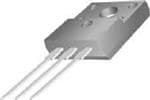
| 供应商器件封装 | TO-220F-6L(成形) |
| 功率(W) | 56W |
| 包装 | 管件 |
| 单位重量 | 1.600 g |
| 占空比-最大 | 87 % |
| 商标 | Fairchild Semiconductor |
| 安装风格 | Through Hole |
| 封装 | Tube |
| 封装/外壳 | TO-220-6 全封装,成形引线 |
| 封装/箱体 | TO-220-6 FP |
| 工作温度 | -25°C ~ 85°C |
| 工作温度范围 | - 25 C to + 85 C |
| 工厂包装数量 | 400 |
| 标准包装 | 50 |
| 电压-击穿 | 650V |
| 电压-输入 | 8 V ~ 20 V |
| 电压-输出 | - |
| 类型 | Current Mode PWM Controllers |
| 系列 | FSDM0465R |
| 输出电压 | 650 V |
| 输出电流 | 2.2 A |
| 输出端数量 | 1 Output |
| 输出隔离 | 隔离 |
| 频率范围 | 60kHz ~ 72kHz |


- 商务部:美国ITC正式对集成电路等产品启动337调查
- 曝三星4nm工艺存在良率问题 高通将骁龙8 Gen1或转产台积电
- 太阳诱电将投资9.5亿元在常州建新厂生产MLCC 预计2023年完工
- 英特尔发布欧洲新工厂建设计划 深化IDM 2.0 战略
- 台积电先进制程称霸业界 有大客户加持明年业绩稳了
- 达到5530亿美元!SIA预计今年全球半导体销售额将创下新高
- 英特尔拟将自动驾驶子公司Mobileye上市 估值或超500亿美元
- 三星加码芯片和SET,合并消费电子和移动部门,撤换高东真等 CEO
- 三星电子宣布重大人事变动 还合并消费电子和移动部门
- 海关总署:前11个月进口集成电路产品价值2.52万亿元 增长14.8%


PDF Datasheet 数据手册内容提取
Is Now Part of To learn more about ON Semiconductor, please visit our website at www.onsemi.com Please note: As part of the Fairchild Semiconductor integration, some of the Fairchild orderable part numbers will need to change in order to meet ON Semiconductor’s system requirements. Since the ON Semiconductor product management systems do not have the ability to manage part nomenclature that utilizes an underscore (_), the underscore (_) in the Fairchild part numbers will be changed to a dash (-). This document may contain device numbers with an underscore (_). Please check the ON Semiconductor website to verify the updated device numbers. The most current and up-to-date ordering information can be found at www.onsemi.com. Please email any questions regarding the system integration to Fairchild_questions@onsemi.com. ON Semiconductor and the ON Semiconductor logo are trademarks of Semiconductor Components Industries, LLC dba ON Semiconductor or its subsidiaries in the United States and/or other countries. ON Semiconductor owns the rights to a number of patents, trademarks, copyrights, trade secrets, and other intellectual property. A listing of ON Semiconductor’s product/patent coverage may be accessed at www.onsemi.com/site/pdf/Patent-Marking.pdf. ON Semiconductor reserves the right to make changes without further notice to any products herein. ON Semiconductor makes no warranty, representation or guarantee regarding the suitability of its products for any particular purpose, nor does ON Semiconductor assume any liability arising out of the application or use of any product or circuit, and specifically disclaims any and all liability, including without limitation special, consequential or incidental damages. Buyer is responsible for its products and applications using ON Semiconductor products, including compliance with all laws, regulations and safety requirements or standards, regardless of any support or applications information provided by ON Semiconductor. “Typical” parameters which may be provided in ON Semiconductor data sheets and/or specifications can and do vary in different applications and actual performance may vary over time. All operating parameters, including “Typicals” must be validated for each customer application by customer’s technical experts. ON Semiconductor does not convey any license under its patent rights nor the rights of others. ON Semiconductor products are not designed, intended, or authorized for use as a critical component in life support systems or any FDA Class 3 medical devices or medical devices with a same or similar classification in a foreign jurisdiction or any devices intended for implantation in the human body. Should Buyer purchase or use ON Semiconductor products for any such unintended or unauthorized application, Buyer shall indemnify and hold ON Semiconductor and its officers, employees, subsidiaries, affiliates, and distributors harmless against all claims, costs, damages, and expenses, and reasonable attorney fees arising out of, directly or indirectly, any claim of personal injury or death associated with such unintended or unauthorized use, even if such claim alleges that ON Semiconductor was negligent regarding the design or manufacture of the part. ON Semiconductor is an Equal Opportunity/Affirmative Action Employer. This literature is subject to all applicable copyright laws and is not for resale in any manner.
F S D M 0 October 2007 4 6 5 R E , F FSDM0465RE, FSDM0565RE, FSDM07652RE S D M Green Mode Fairchild Power Switch (FPS™) 0 5 6 5 Features Description R E (cid:132) Internal Avalanche-Rugged SenseFET The FSDM0465RE, FSDM0565RE and FSDM07652RE , F (cid:132) Advanced Burst-Mode Operation Consumes Under are an integrated Pulse Width Modulator (PWM) and S 1W at 240V & 0.5W load SenseFET specifically designed for high-performance D AC M offline Switch Mode Power Supplies (SMPS) with (cid:132) Precision Fixed Operating Frequency (66kHz) 0 minimal external components. This device is an 7 (cid:132) Internal Start-up Circuit integrated high-voltage power-switching regulator that 6 5 (cid:132) Improved Pulse-by-Pulse Current Limiting combines an avalanche-rugged SenseFET with a 2 R (cid:132) Over-Voltage Protection (OVP) current mode PWM control block. The PWM controller E (cid:132) Overload Protection (OLP) includes an integrated fixed-frequency oscillator, under- — (cid:132) Internal Thermal Shutdown Function (TSD) voltage lockout, leading-edge blanking (LEB), optimized gate driver, internal soft-start, temperature-compensated G (cid:132) Auto-Restart Mode r precise-current sources for a loop compensation, and e (cid:132) Under-Voltage Lockout (UVLO) with hysteresis e self-protection circuitry. Compared with a discrete n (cid:132) Low Operating Current (2.5mA) MOSFET and PWM controller solution, it can reduce total M (cid:132) Built-in Soft-Start cost; component count, size, and weight; while o simultaneously increasing efficiency, productivity, and d e system reliability. This device is a basic platform well F Applications suited for cost-effective designs of flyback converters. a i (cid:132) SMPS for LCD monitor and STB rc h (cid:132) Adaptor i l d P o w e r S w i t c h ( F P Ordering Information S ™ ) Product Number Package Marking Code BV R Max. DSS DS(ON) FSDM0465REWDTU(1) TO-220F-6L (Forming) DM0465RE 650V 2.6 Ω FSDM0565REWDTU TO-220F-6L (Forming) DM0565RE 650V 2.2 Ω FSDM07652REWDTU TO-220F-6L (Forming) DM07652RE 650V 1.6 Ω Note: 1. WDTU: Forming Type. All packages are lead free per JEDEC: J-STD-020B standard. FPSTM is a trademark of Fairchild Semiconductor Corporation. © 2006 Fairchild Semiconductor Corporation www.fairchildsemi.com FSDM0465RE, FSDM0565RE, FSDM07652RE Rev. 1.0.2
F S Typical Circuit D M 0 4 6 5 R AC E IN DC , OUT F S D M 0 Vstr Drain 5 6 5 R PWM E , F FB VCC Source S D M 0 7 6 5 2 FSDM0565RE Rev: 00 R E Figure 1. Typical Flyback Application — G r e e n Output Power Table M o 230VAC ±15%(4) 85–265VAC d Product e Adapter(2) Open Frame(3) Adapter(2) Open Frame(3) F a FSDM0465RE 48W 56W 40W 48W i r c FSDM0565RE 60W 70W 50W 60W h i l FSDM07652RE 70W 80W 60W 70W d P Notes: o w 2. Typical continuous power in a non-ventilated enclosed adapter measured at 50°C ambient. e 3. Maximum practical continuous power in an open-frame design at 50°C ambient. r S 4. 230VAC or 100/115VAC with doubler. w i t c h ( F P S ™ ) © 2006 Fairchild Semiconductor Corporation www.fairchildsemi.com FSDM0465RE, FSDM0565RE, FSDM07652RE Rev. 1.0.2 2
F S Internal Block Diagram D M 0 4 VCC Vstr Drain 65 3 6 1 R E , NC 5 I F start S 0.5/0.7V + Internal D Vref Bias M - 8V/12V VCC good 0 5 6 V V 5 CC ref R OSC E Idelay IFB 2.5R PWM S Q , F FB 4 S Gate D R Q driver M Soft-start R 0 7 LEB 6 5 2 R V E SD — V 2 GND CC G S Q r V e ovp e V good R Q V n TSD CC CL M o d FSDM0565RE Rev: 00 e F Figure 2. Functional Block Diagram of FSDM0x65RE a i r c h i l d P o w e r S w i t c h ( F P S ™ ) © 2006 Fairchild Semiconductor Corporation www.fairchildsemi.com FSDM0465RE, FSDM0565RE, FSDM07652RE Rev. 1.0.2 3
F S Pin Configuration D M 0 4 6 5 R TO-220F-6L E , F 6. Vstr S 5. NC D M 4. FB 0 3. VCC 5 2. GND 6 5 1. Drain R E , F Figure 3. Pin Configuration (Top View) S D M 0 7 Pin Definitions 6 5 2 Pin # Name Description R E SenseFET drain. This pin is the high-voltage power SenseFET drain. It is de- 1 Drain — signed to drive the transformer directly. G 2 GND Ground. This pin is the control ground and the SenseFET source. r e Power Supply. This pin is the positive supply voltage input. During start-up, e n the power is supplied by an internal high-voltage current source connected to 3 VCC the V pin. When V reaches 12V, the internal high-voltage current source M str CC o is disabled and the power is supplied from the auxiliary transformer winding. d e Feedback. This pin is internally connected to the inverting input of the PWM F comparator. The collector of an opto-coupler is typically tied to this pin. For a i 4 FB stable operation, a capacitor should be placed between this pin and GND. If r c the voltage of this pin reaches 6.0V, the overload protection is activated, re- h i sulting in shutdown of the FPS™. ld 5 NC No Connection. P o Start-up. This pin is connected directly to the high-voltage DC link. At start-up, w the internal high-voltage current source supplies internal bias and charges the e 6 V r str external capacitor connected to the VCC pin. Once VCC reaches 12V, the in- S ternal current source is disabled. w i t c h ( F P S ™ ) © 2006 Fairchild Semiconductor Corporation www.fairchildsemi.com FSDM0465RE, FSDM0565RE, FSDM07652RE Rev. 1.0.2 4
F S Absolute Maximum Ratings D M The “Absolute Maximum Ratings” are those values beyond which the safety of the device cannot be guaranteed. The 0 device should not be operated at these limits. The parametric values defined in the Electrical Characteristics tables 4 6 are not guaranteed at the absolute maximum ratings. T = 25°C, unless otherwise specified. 5 A R Symbol Parameter Value Unit E , F BV Drain Source Breakdown Voltage 650 V DSS S D V Max. Voltage at Vstart pin 650 V str M FSDM0465RE T =25°C 9.6 0 C 5 I Drain Current Pulsed(5) FSDM0565RE T =25°C 11 A 6 DM C DC 5 R FSDM07652RE T =25°C 15 C E FSDM0465RE TC=25°C 2.2 , F T =100°C 1.4 S C D T =25°C 2.8 M C ID Continuous Drain Current FSDM0565RE A 0 TC=100°C 1.7 7 6 T =25°C 3.8 5 FSDM07652RE C 2 T =100°C 2.4 R C E FSDM0465RE — EAS Single Pulsed Avalanche Energy(6) FSDM0565RE 190 mJ G FSDM07652RE 370 re e V Supply Voltage 20 V n CC M V Input Voltage Range -0.3 to V V FB CC o P (Watt H/S) Total Power Dissipation (T =25°C) 45 W d D C e T Operating Junction Temperature Internally limited °C F J a TA Operating Ambient Temperature -25 to +85 °C ir c T Storage Temperature -55 to +150 °C h STG i l ESD Capability, HBM Model 2.0 d kV (All pins except V and FB) (GND-V /V =1.5kV) P str str FB o ESD Capability, Machine Model 300 w V e (All pins except V and FB) (GND-V /V =225V) str str FB r S Notes: w 5. Repetitive rating: Pulse width limited by maximum junction temperature. it c 6. L=14mH, starting T =25°C. h J ( F P Thermal Impedance S ™ ) T =25°C, unless otherwise specified. A Symbol Parameter Value Unit θ (7) Junction-to-Ambient Thermal Resistance 49.90 °C/W JA θ (8) Junction-to-Case Thermal Resistance 2.78 °C/W JC Notes: 7. Free-standing, with no heat-sink, under natural convection. 8. Infinite cooling condition - refer to the SEMI G30-88. © 2006 Fairchild Semiconductor Corporation www.fairchildsemi.com FSDM0465RE, FSDM0565RE, FSDM07652RE Rev. 1.0.2 5
F S Electrical Characteristics D M T = 25°C unless otherwise specified. 0 A 4 6 Symbol Parameter Condition Min. Typ. Max. Unit 5 R SenseFET SECTION E , V = 650V, V = 0V 250 F FSDM0465RE DS GS S V = 520V, V = 0V, T = 125°C 250 D DS GS C M Zero Gate Voltage VDS = 650V, VGS = 0V 500 0 IDSS Drain Current FSDM0565RE V = 520V, V = 0V, T = 125°C 500 µA 56 DS GS C 5 V = 650V, V = 0V 500 R DS GS FSDM07652RE E V = 520V, V = 0V, T = 125°C 500 , DS GS C F FSDM0465RE 2.20 2.60 S Static Drain Source D RDS(ON) on Resistance(9) FSDM0565RE VGS = 10V, ID = 2.5A 1.76 2.20 Ω M 0 FSDM07652RE 1.40 1.60 7 6 FSDM0465RE 60 5 2 C Output Capacitance FSDM0565RE V = 0V, V = 25V, f = 1MHz 78 pF R OSS GS DS E FSDM07652RE 100 — FSDM0465RE 23 G t Turn-On Delay Time FSDM0565RE V = 325V, I = 5A 22 ns r d(on) DD D e e FSDM07652RE 22 n FSDM0465RE 20 M o t Rise Time FSDM0565RE V = 325V, I = 5A 52 ns d r DD D e FSDM07652RE 60 F a FSDM0465RE 65 i r c td(off) Turn-Off Delay Time FSDM0565RE VDD = 325V, ID = 5A 95 ns h i l FSDM07652RE 115 d P FSDM0465RE 27 o w t Fall Time FSDM0565RE V = 325V, I = 5A 50 ns f DD D e r FSDM07652RE 65 S CONTROL SECTION w i t f Switching Frequency V = 3V 60 66 72 kHz c OSC FB h ΔfSTABLE Switching Frequency Stability 13V ≤ VCC ≤ 18V 0 1 3 % (F Δf Switching Frequency Variation(10) -25°C ≤ T ≤ 85°C 0 ±5 ±10 % P OSC A S I Feedback Source Current V = GND 0.7 0.9 1.1 mA ™ FB FB ) FSDM0465RE 77 82 87 % D Maximum Duty Cycle FSDM0565RE 77 82 87 % MAX FSDM07652RE 75 80 85 % D Minimum Duty Cycle 0 % MIN V V = GND 11 12 13 V START FB UVLO Threshold Voltage V V = GND 7 8 9 V STOP FB t Internal Soft-Start Time V = 3 10 15 ms S/S FB © 2006 Fairchild Semiconductor Corporation www.fairchildsemi.com FSDM0465RE, FSDM0565RE, FSDM07652RE Rev. 1.0.2 6
F S Electrical Characteristics (Continued) D M T = 25°C unless otherwise specified. 0 A 4 6 Symbol Parameter Condition Min. Typ. Max. Unit 5 R BURST MODE SECTION E , V V = 14V 0.7 V F BURH Burst Mode Voltages CC S V V = 14V 0.5 V D BURL CC M PROTECTION SECTION 0 5 V Shutdown Feedback Voltage V ≥ 5.5V 5.5 6.0 6.5 V 6 SD FB 5 I Shutdown Delay Current V = 5V 2.8 3.5 4.2 µA R DELAY FB E t Leading-Edge Blanking Time 250 ns , LEB F FSDM0465RE V = 5V, V = 14V 1.60 1.80 2.00 S FB CC D ILIMIT Peak Current Limit(11) FSDM0565RE VFB = 5V, VCC = 14V 2.00 2.25 2.50 A M 0 FSDM07652RE VFB = 5V, VCC = 14V 2.20 2.50 2.70 7 6 VOVP Over-Voltage Protection 18 19 20 V 5 2 T Thermal Shutdown Temperature(10) 130 145 160 °C R SD E TOTAL DEVICE SECTION — IOP VFB = GND, VCC = 14V G I Operating Supply Current(12) V = GND, V = 10V 2.5 5.0 mA r OP(MIN) FB CC e e IOP(MAX) VFB = GND, VCC = 18V n M Notes: o 9. Pulse test: Pulse width ≤ 300µS, duty cycle ≤ 2%. d e 10. These parameters, although guaranteed at the design, are not tested in production. F 11. These parameters indicate the inductor current. a i r 12. This parameter is the current flowing into the control IC. c h i l d P o w e r S w i t c h ( F P S ™ ) © 2006 Fairchild Semiconductor Corporation www.fairchildsemi.com FSDM0465RE, FSDM0565RE, FSDM07652RE Rev. 1.0.2 7
F S Comparison Between FS6M0765RTC and FSDM0x65RE D M 0 4 Function FS6M0765RTC FSDM0x65RE FSDM0x65RE Advantages 6 5 R (cid:132) Gradually increasing current limit during E soft-start reduces peak current and volt- , Adjustable soft-start Internal soft-start with F age component stresses S Soft-Start time using an external typically 10ms (fixed) (cid:132) Eliminates external soft-start components D capacitor M in most applications 0 (cid:132) Reduces or eliminates output overshoot 5 6 (cid:132) Built into controller (cid:132) Built into controller (cid:132) Improves light-load efficiency 5 R Burst-Mode Operation (cid:132) Output voltage (cid:132) Output voltage fixed (cid:132) Reduces no-load consumption E drops to around half , F S D M 0 7 6 5 2 R E — G r e e n M o d e F a i r c h i l d P o w e r S w i t c h ( F P S ™ ) © 2006 Fairchild Semiconductor Corporation www.fairchildsemi.com FSDM0465RE, FSDM0565RE, FSDM07652RE Rev. 1.0.2 8
F S Typical Performance Characteristics D M These characteristic graphs are normalized at TA= 25°C. 0 4 6 5 R 1.2 1.2 E , 1.0 e 1.0 F Operating Current (I)op 000...468 art Thershold Voltag (V)start 000...468 SDM0565R 0.2 St 0.2 E , F 0.0 0.0 S -25 0 25 50 75 100 125 150 -25 0 25 50 75 100 125 150 D M Junction Temperature [°C] Junction Temperature [°C] 0 7 6 5 2 Figure 4. Operating Current vs. Temp. Figure 5. Start Threshold Voltage vs. Temp. R E — G 1.2 1.2 r e e 1.0 1.0 e Voltag 0.8 uency 0.8 n M Stop Threshold (V)stop 000...246 Operating Freq (f)osc 000...246 ode Fair c h 0.0 0.0 i l d -25 0 25 50 75 100 125 150 -25 0 25 50 75 100 125 150 P Junction Temperature [°C] Junction Temperature [°C] o w e r S Figure 6. Stop Threshold Voltage vs. Temp. Figure 7. Operating Frequency vs. Temp. w i t c h 1.2 1.2 (F P 1.0 1.0 S e um Duty Cycl (D)MAX 00..68 ource Current (I)FB 00..68 ™) m 0.4 S 0.4 xi B a F M 0.2 0.2 0.0 0.0 -25 0 25 50 75 100 125 150 -25 0 25 50 75 100 125 150 Junction Temperature [°C] Junction Temperature [°C] Figure 8. Maximum Duty Cycle vs. Temp. Figure 9. Feedback Source Current vs. Temp. © 2006 Fairchild Semiconductor Corporation www.fairchildsemi.com FSDM0465RE, FSDM0565RE, FSDM07652RE Rev. 1.0.2 9
F S Typical Performance Characteristics (Continued) D M These characteristic graphs are normalized at TA= 25°C. 0 4 6 5 R 1.2 1.2 E , oltage 01..80 Current 01..80 FSD utdown FB V (V)SD 00..46 down Delay (I)DELAY 00..46 M0565R Sh 0.2 Shut 0.2 E , F 0.0 0.0 S -25 0 25 50 75 100 125 150 -25 0 25 50 75 100 125 150 D M Junction Temperature [°C] Junction Temperature [°C] 0 7 6 5 2 Figure 10. Shutdown Feedback Voltage vs. Temp. Figure 11. Shutdown Delay Current vs. Temp. R E — G 1.2 1.2 e r g e a otection 01..80 able Volt 01..80 en M Over-Voltage Pr (V)ovp 000...246 B Burst-Mode En (V)FBE 000...246 ode Fairc F h 0.0 0.0 i l d -25 0 25 50 75 100 125 150 -25 0 25 50 75 100 125 150 P Junction Temperature [°C] Junction Temperature [°C] o w e r S Figure 12. Over-Voltage Protection vs. Temp. Figure 13. Burst-Mode Enable Voltage vs. Temp. w i t c h 1.2 1.2 (F e g P a olt 1.0 1.0 S Burst-Mode Disable V (V)FBD 0000....2468 Peak Current Limit (Self protection) (I)over 0000....2468 ™) B F 0.0 0.0 -25 0 25 50 75 100 125 150 -50 -25 0 25 50 75 100 125 Junction Temperature [°C] Junction Temperature [°C] Figure 14. Burst-Mode Disable Voltage vs. Temp. Figure 15. Current Limit vs. Temp. © 2006 Fairchild Semiconductor Corporation www.fairchildsemi.com FSDM0465RE, FSDM0565RE, FSDM07652RE Rev. 1.0.2 10
F S Typical Performance Characteristics (Continued) D M These characteristic graphs are normalized at TA= 25°C. 0 4 6 5 R 1.2 E , 1.0 F C) S Time o 25° 0.8 DM oft-Start malized t 00..46 0565 S or R N ( 0.2 E , F 0.0 S -50 -25 0 25 50 75 100 125 D M Junction Temperature [°C] 0 7 6 5 2 Figure 16. Soft-Start Time vs. Temp. R E — G r e e n M o d e F a i r c h i l d P o w e r . S w i t c h ( F P S ™ ) © 2006 Fairchild Semiconductor Corporation www.fairchildsemi.com FSDM0465RE, FSDM0565RE, FSDM07652RE Rev. 1.0.2 11
F S Functional Description 2.1 Pulse-by-Pulse Current Limit: Because current- D mode control is employed, the peak current through the M 1. Start-up: In previous generations of Fairchild Power 0 Switches (FPS™), the V pin had an external start-up SenseFET is limited by the inverting input of PWM 4 CC comparator (V *) as shown in Figure 18. Assuming that 6 resistor to the DC input voltage line. In this generation, FB 5 the 0.9mA current source flows only through the internal R the start-up resistor is replaced by an internal high- E resistor (2.5R + R = 2.8kΩ), the cathode voltage of diode voltage current source. At start-up, the internal high- , D2 is about 2.5V. Since D1 is blocked when the feedback F voltage current source supplies the internal bias and S voltage (V ) exceeds 2.5V, the maximum voltage of the charges the external capacitor (C ) connected to the FB D vcc cathode of D2 is clamped at this voltage, thus clamping M V pin, as illustrated in Figure 17. When V reaches CC CC V *. Therefore, the peak value of the current through 0 12V, the FSDM0x65RE begins switching and the internal FB 5 the SenseFET is limited. 6 high-voltage current source is disabled. The 5 FSDM0x65RE continues normal switching operation and 2.2 Leading Edge Blanking (LEB): At the instant the R E the power is supplied from the auxiliary transformer internal SenseFET is turned on, a high-current spike , winding unless V goes below the stop voltage of 8V. occurs through the SenseFET, caused by primary-side F CC S capacitance and secondary-side rectifier reverse D recovery. Excessive voltage across the Rsense resistor M would lead to incorrect feedback operation in the current 0 7 mode PWM control. To counter this effect, the 6 5 FSDM0x65RE employs a leading-edge blanking (LEB) 2 circuit. This circuit inhibits the PWM comparator for a R V E DC short time (tLEB) after the SenseFET is turned on. — G C Vcc r e e VCC Vref n VCC 3 6 Vstr VO VFB 4Idelay IFB OSC SenseFET Mod H11A817A D1 D2 e CB 2.5R I F start + Gate a Vfb* R driver ir Vref KA431 - c 8V/12V V good h CC i l d Internal V OLP Rsense P Bias SD o FSDM0565RE Rev: 00 w FSDM0565RE Rev: 00 e Figure 18. Pulse-Width-Modulation (PWM) Circuit r Figure 17. Internal Start-up Circuit S w i t c 3. Protection Circuit: The FSDM0x65RE has several h self-protective functions, such as overload protection (F 2. Feedback Control: FSDM0x65RE employs current- (OLP), over-voltage protection (OVP), and thermal P S mode control, as shown in Figure 18. An opto-coupler shutdown (TSD). Because these protection circuits are ™ (such as the H11A817A) and shunt regulator (such as fully integrated into the IC without external components, ) the KA431) are typically used to implement the feedback the reliability is improved without increasing cost. Once a network. Comparing the feedback voltage with the fault condition occurs, switching is terminated and the voltage across the Rsense resistor, plus an offset voltage, SenseFET remains off, which causes VCC to fall. When makes it possible to control the switching duty cycle. V reaches the UVLO stop voltage of 8V, the protection CC When the reference pin voltage of the shunt regulator is reset and the internal high-voltage current source exceeds the internal reference voltage of 2.5V, the opto- charges the V capacitor via the V pin. When V CC str CC coupler LED current increases, pulling down the reaches the UVLO start voltage of 12V, the feedback voltage and reducing the duty cycle. This event FSDM0x65RE resumes normal operation. In this typically occurs when the input voltage is increased or manner, the auto-restart can alternately enable and the output load is decreased. disable the switching of the power SenseFET until the fault condition is eliminated (see Figure 19). © 2006 Fairchild Semiconductor Corporation www.fairchildsemi.com FSDM0465RE, FSDM0565RE, FSDM07652RE Rev. 1.0.2 12
F S D M Fault V FSDM0565RE Rev: 00 0 VDS Poowner occurs reFmaouvlted FB Overload protection 465 R E 6.0V , F S D M 2.5V 0 5 V 6 CC 5 T = C *(6.0-2.5)/I R 12 FB delay E 12V , T T t F 8V 1 2 S D M Figure 20. Overload Protection t 0 7 6 Normal Fault Normal 5 FSDM0565RE Rev: 00 operation situation operation 3si.d2e Ofeveedr-bVaoclkta gceir cPuirto wteecrteio tno (mOaVlPfu)n: cItfi otnh eo rs eac osnodldaeryr 2R E defect caused an opening in the feedback path, the Figure 19. Auto Restart Operation — current through the opto-coupler transistor becomes almost zero. In this event, V climbs in a similar manner G FB r to the overload situation, forcing the preset maximum e 3.1 Overload Protection (OLP): Overload is defined as current to be supplied to the SMPS until the overload e n the load current exceeding a pre-set level due to an protection is activated. Because more energy than M unexpected event. In this situation, the protection circuit required is provided to the output, the output voltage may o should be activated to protect the SMPS. Even when the exceed the rated voltage before the overload protection d SMPS is in normal operation, the overload protection is activated, resulting in the breakdown of the devices in e F circuit can be activated during the load transition. To the secondary side. To prevent this situation, an over- a avoid this undesired operation, the overload protection voltage protection (OVP) circuit is employed. In general, ir c circuit is designed to be activated after a specified time V is proportional to the output voltage and the h CC to determine whether it is a transient situation or a true FSDM0x65RE uses VCC instead of directly monitoring ild overload situation. Because of the pulse-by-pulse the output voltage. If V exceeds 19V, an OVP circuit is P current limit capability, the maximum peak current CC o through the SenseFET is limited, and therefore the activated, resulting in the termination of the switching w maximum input power is restricted with a given input operation. To avoid undesired activation of OVP during e r voltage. If the output consumes beyond this maximum normal operation, VCC should be designed below 19V. S power, the output voltage (V ) decreases below the set w O 3.3 Thermal Shutdown (TSD): The SenseFET and the i voltage. This reduces the current through the opto- control IC are built in one package. This makes it easy tc coupler LED, which also reduces the opto-coupler for the control IC to detect the heat generation from the h transistor current, thus increasing the feedback voltage SenseFET. When the temperature exceeds ~150°C, the (F (VFB). If VFB exceeds 2.5V, D1 is blocked and the 3.5µA thermal shutdown is activated. PS current source starts to charge CB slowly up to VCC. In 4. Soft-Start: The FSDM0x65RE has an internal soft- ™ this condition, V continues increasing until it reaches ) FB start circuit that increases PWM comparator inverting 6V, when the switching operation is terminated, as input voltage, together with the SenseFET current, shown in Figure 20. The delay time for shutdown is the slowly after it starts up. The typical soft-start time is time required to charge CB from 2.5V to 6.0V with 3.5µA. 10ms. The pulse width to the power switching device is A 10 ~ 50ms delay time is typical for most applications. progressively increased to establish the correct working conditions for transformers, inductors, and capacitors. The voltage on the output capacitors is progressively increased with the intention of smoothly establishing the required output voltage. It also helps prevent transformer saturation and reduces the stress on the secondary diode during start-up. © 2006 Fairchild Semiconductor Corporation www.fairchildsemi.com FSDM0465RE, FSDM0565RE, FSDM07652RE Rev. 1.0.2 13
F S 5. Burst Operation: To minimize power dissipation in D standby mode, the FSDM0x65RE enters burst-mode M 0 operation. As the load decreases, the feedback voltage 4 decreases. As shown in Figure 21, the device 6 5 automatically enters burst mode when the feedback R voltage drops below V (500mV). At this point, E BURL , switching stops and the output voltages start to drop at a F S rate dependent on standby current load. This causes the D feedback voltage to rise. Once it passes VBURH (700mV), M switching resumes. The feedback voltage then falls and 0 5 the process repeats. Burst-mode operation alternately 6 enables and disables switching of the power SenseFET, 5 R thereby reducing switching loss in standby mode. E , F S D M Vo 0 V set 7 O 6 5 2 R V E FB — 0.7V G 0.5V r e e n I DS M o d e F a i VDS rc h i l d P o time w Switching Switching e FSDM0565RE Rev: 00 T1 disabled T2 T3 disabled T4 r S w Figure 21. Waveforms of Burst Operation i t c h ( F P S ™ ) © 2006 Fairchild Semiconductor Corporation www.fairchildsemi.com FSDM0465RE, FSDM0565RE, FSDM07652RE Rev. 1.0.2 14
F S Application Information D M 0 4 Application Output Power Input Voltage Output Voltage (Max. Current) 6 5 R Universal input 5V (2.0A) LCD Monitor 40W E (85-265VAC) 12V (2.5A) , F S D M Features 0 5 (cid:132) High efficiency (>81% at 85VAC input) 6 5 (cid:132) Low zero load power consumption (<300mW at 240VAC input) R (cid:132) Low standby mode power consumption (<800mW at 240VAC input and 0.3W load) E, (cid:132) Low component count F S (cid:132) Enhanced system reliability through various protection functions D (cid:132) Internal soft-start (10ms) M 0 7 Key Design Notes 6 5 (cid:132) Resistors R102 and R105 are employed to prevent start-up at low input voltage. After start-up, there is no power 2 R loss in these resistors since the start-up pin is internally disconnected after start-up. E (cid:132) The delay time for overload protection is designed to be about 50ms with C106 of 47nF. If a faster triggering of OLP — is required, C106 can be reduced to 10nF. G (cid:132) Zener diode ZD102 is used for a safety test, such as UL. When the drain pin and feedback pin are shorted, the r zener diode fails and remains short, which causes the fuse (F1) to be blown and prevents explosion of the opto-cou- e e pler (IC301). This zener diode also increases the immunity against line surge. n M o d 1. Schematic e F a T1 D202 L201 i EER3016 MBRF10100 12V, 2.5A rc 1 10 C201 C202 h 1000μF 1000μF il C103 R301k0Ω2 R5261Wk0Ω3 2C1.12k0nV4F D101 2 8 25V 25V d Po 140000μVF UF 4007 3 w 2KBPB0D61M031N2572 R401k0Ω5 FSDMIC05165RE er S 1 3 6Vstr Drain1 w 227C25410V0nA2FC Z1D01V02 C45710n0VF6 54FNBCGND2VCZC2D213V01 C25210μ0VF5UDF1400204 R51Ω04 4 76MBD1RC021F00201010V0μ34F5 L2021C0102000Vμ4F 5V, 2A itch (FP 5 S ™ C301 ) LF101 4.7nF 23mH R201 1kΩ R101 R204 560kΩ 5.6kΩ 1W 1R.22k0Ω2 R122k0Ω3 C472n0F5 IC301 5RDT-19 2 72C521V00nA1FC F25FU01SVE H11A817A KICA240311 5R.620kΩ5 2A FSDM0565RE Rev: 00 Figure 22. Demo Circuit © 2006 Fairchild Semiconductor Corporation www.fairchildsemi.com FSDM0465RE, FSDM0565RE, FSDM07652RE Rev. 1.0.2 15
F S 2. Transformer D M 0 4 6 EER3016 5 1 10 R N/2 N p 12V E , 2 9 F Np/2 S D 3 8 M 0 5 4 7 N 6 5V 5 R N 5 6 E a , FSDM0565RE Rev: 00 F S D Figure 23. Transformer Schematic Diagram M 0 7 6 5 2 3. Winding Specification R E — No Pin (s→f) Wire Turns Winding Method G N 4 → 5 0.2φ × 1 8 Center Winding re a e Insulation: Polyester Tape t = 0.050mm, 2 Layers n M N /2 2 → 1 0.4φ × 1 18 Solenoid Winding p o d Insulation: Polyester Tape t = 0.050mm, 2 Layers e N 10 → 8 0.3φ × 3 7 Center Winding F 12V a Insulation: Polyester Tape t = 0.050mm, 2 Layers ir c N 7 → 6 0.3φ × 3 3 Center Winding h 5V i l d Insulation: Polyester Tape t = 0.050mm, 2 Layers P N /2 3 → 2 0.4φ × 1 18 Solenoid Winding o p w Outer Insulation: Polyester Tape t = 0.050mm, 2 Layers e r S w i t c h 4. Electrical Characteristics ( F P S ™ Pin Specification Remarks ) Inductance 1 - 3 520µH ± 10% 100kHz, 1V Leakage Inductance 1 - 3 10µH Max 2nd all short 5. Core & Bobbin (cid:132) Core: EER 3016 (cid:132) Bobbin: EER3016 (cid:132) Ae(mm2): 96 © 2006 Fairchild Semiconductor Corporation www.fairchildsemi.com FSDM0465RE, FSDM0565RE, FSDM07652RE Rev. 1.0.2 16
F S 6. Demo Circuit Part List D M 0 4 Part Value Note Part Value Note 6 5 R Fuse D102 UF4004 E , F101 2A/250V D201 MBRF1045 F S D202 MBRF10100 D NTC ZD101 Zener Diode 22V M 0 RT101 5D-9 ZD102 Zener Diode 10V 5 6 5 R Resistor Bridge Diode E , R101 560kΩ 1W BD101 2KBP06M 3N257 Bridge Diode F S R102 30kΩ 1/4W D M R103 56kΩ 2W Line Filter 0 7 R104 5Ω 1/4W LF101 23mH Wire 0.4mm 6 5 R105 40kΩ 1/4W 2 R R201 1kΩ 1/4W IC E — R202 1.2kΩ 1/4W IC101 FSDM0565RE FPS™ (5A,650V) G R203 12kΩ 1/4W IC201 KA431 (TL431) Voltage reference r e R204 5.6kΩ 1/4W IC301 H11A817A Opto-coupler e n R205 5.6kΩ 1/4W M o d Capacitor e F C101 220nF/275V Box Capacitor a AC i r C102 220nF/275V Box Capacitor c AC h C103 100µF/400V Electrolytic Capacitor il d C104 2.2nF/1kV Ceramic Capacitor P o C105 22µF/50V Electrolytic Capacitor w e C106 47nF/50V Ceramic Capacitor r S C201 1000µF/25V Electrolytic Capacitor w C202 1000µF/25V Electrolytic Capacitor it c h C203 1000µF/10V Electrolytic Capacitor ( F C204 1000µF/10V Electrolytic Capacitor P S C205 47nF/50V Ceramic Capacitor ™ C301 4.7nF Polyester Film Cap. ) Inductor L201 5µH Wire 1.2mm L202 5µH Wire 1.2mm Diode D101 UF4007 © 2006 Fairchild Semiconductor Corporation www.fairchildsemi.com FSDM0465RE, FSDM0565RE, FSDM07652RE Rev. 1.0.2 17
F S 7. Layout D M 0 4 6 5 R E , F S D M 0 5 6 5 R E , F S D M 0 7 6 5 2 R E — G r e e n M Figure 24. Layout Considerations for FSDM0565RE (Top View) o d e F a i r c h i l d P o w e r S w i t c h ( F P S ™ ) Figure 25. Layout Considerations for FSDM0565RE (Bottom View) © 2006 Fairchild Semiconductor Corporation www.fairchildsemi.com FSDM0465RE, FSDM0565RE, FSDM07652RE Rev. 1.0.2 18
F S Package Dimensions D M 0 4 6 5 R E , F S D M 0 5 6 5 R E , F S D M 0 7 6 5 2 R E — G r e e n M o d e F a i r c h i l d P o w e r S w i t c h ( F P S ™ ) Figure 26. TO-220F-6L (Forming) © 2006 Fairchild Semiconductor Corporation www.fairchildsemi.com FSDM0465RE, FSDM0565RE, FSDM07652RE Rev. 1.0.2 19
F S D M 0 4 6 5 R E , F S D M 0 5 6 5 R E , F S D M 0 7 6 5 2 R E — G r e e n M o d e F a i r c h i l d P o w e r S w i t c h ( F P S ™ ) © 2006 Fairchild Semiconductor Corporation www.fairchildsemi.com FSDM0465RE, FSDM0565RE, FSDM07652RE Rev. 1.0.2 20
ON Semiconductor and are trademarks of Semiconductor Components Industries, LLC dba ON Semiconductor or its subsidiaries in the United States and/or other countries. ON Semiconductor owns the rights to a number of patents, trademarks, copyrights, trade secrets, and other intellectual property. A listing of ON Semiconductor’s product/patent coverage may be accessed at www.onsemi.com/site/pdf/Patent−Marking.pdf. ON Semiconductor reserves the right to make changes without further notice to any products herein. ON Semiconductor makes no warranty, representation or guarantee regarding the suitability of its products for any particular purpose, nor does ON Semiconductor assume any liability arising out of the application or use of any product or circuit, and specifically disclaims any and all liability, including without limitation special, consequential or incidental damages. Buyer is responsible for its products and applications using ON Semiconductor products, including compliance with all laws, regulations and safety requirements or standards, regardless of any support or applications information provided by ON Semiconductor. “Typical” parameters which may be provided in ON Semiconductor data sheets and/or specifications can and do vary in different applications and actual performance may vary over time. All operating parameters, including “Typicals” must be validated for each customer application by customer’s technical experts. ON Semiconductor does not convey any license under its patent rights nor the rights of others. ON Semiconductor products are not designed, intended, or authorized for use as a critical component in life support systems or any FDA Class 3 medical devices or medical devices with a same or similar classification in a foreign jurisdiction or any devices intended for implantation in the human body. Should Buyer purchase or use ON Semiconductor products for any such unintended or unauthorized application, Buyer shall indemnify and hold ON Semiconductor and its officers, employees, subsidiaries, affiliates, and distributors harmless against all claims, costs, damages, and expenses, and reasonable attorney fees arising out of, directly or indirectly, any claim of personal injury or death associated with such unintended or unauthorized use, even if such claim alleges that ON Semiconductor was negligent regarding the design or manufacture of the part. ON Semiconductor is an Equal Opportunity/Affirmative Action Employer. This literature is subject to all applicable copyright laws and is not for resale in any manner. PUBLICATION ORDERING INFORMATION LITERATURE FULFILLMENT: N. American Technical Support: 800−282−9855 Toll Free ON Semiconductor Website: www.onsemi.com Literature Distribution Center for ON Semiconductor USA/Canada 19521 E. 32nd Pkwy, Aurora, Colorado 80011 USA Europe, Middle East and Africa Technical Support: Order Literature: http://www.onsemi.com/orderlit Phone: 303−675−2175 or 800−344−3860 Toll Free USA/Canada Phone: 421 33 790 2910 Fax: 303−675−2176 or 800−344−3867 Toll Free USA/Canada Japan Customer Focus Center For additional information, please contact your local Email: orderlit@onsemi.com Phone: 81−3−5817−1050 Sales Representative © Semiconductor Components Industries, LLC www.onsemi.com www.onsemi.com 1
Mouser Electronics Authorized Distributor Click to View Pricing, Inventory, Delivery & Lifecycle Information: O N Semiconductor: FSDM0465REWDTU