ICGOO在线商城 > 集成电路(IC) > PMIC - AC-DC 转换器,离线开关 > KA5M0380RYDTU
 Datasheet下载
- 型号: KA5M0380RYDTU
- 制造商: Fairchild Semiconductor
- 库位|库存: xxxx|xxxx
- 要求:
| 数量阶梯 | 香港交货 | 国内含税 |
| +xxxx | $xxxx | ¥xxxx |
查看当月历史价格
查看今年历史价格
KA5M0380RYDTU产品简介:
ICGOO电子元器件商城为您提供KA5M0380RYDTU由Fairchild Semiconductor设计生产,在icgoo商城现货销售,并且可以通过原厂、代理商等渠道进行代购。 KA5M0380RYDTU价格参考。Fairchild SemiconductorKA5M0380RYDTU封装/规格:PMIC - AC-DC 转换器,离线开关, Converter Offline Flyback, Forward Topology 67kHz TO-220F-4L (Forming)。您可以下载KA5M0380RYDTU参考资料、Datasheet数据手册功能说明书,资料中有KA5M0380RYDTU 详细功能的应用电路图电压和使用方法及教程。
KA5M0380RYDTU 是一款由 ON Semiconductor(安森美半导体)生产的 PMIC - AC-DC 转换器,属于离线开关类型。它主要用于将交流电(AC)转换为直流电(DC),适用于需要高效、稳定电源转换的场景。以下是该型号的主要应用场景:

1. 消费类电子产品
   - 例如电视、机顶盒、音响设备等需要稳定的 DC 电源供应的产品。这些设备通常需要从市电(AC)转换为适合内部电路运行的低压 DC。

2. 家电产品
   - 包括冰箱、空调、洗衣机等智能家电中,用于控制板或传感器模块的电源供电。KA5M0380RYDTU 的高效率和低待机功耗特性非常适合现代节能型家电。

3. 工业自动化设备
   - 在工业领域,可用于 PLC(可编程逻辑控制器)、传感器接口、数据采集系统等设备的电源模块。其可靠的性能确保了工业设备在复杂环境下的稳定运行。

4. LED 照明驱动
   - 该芯片可以为 LED 照明系统提供高效的电源转换解决方案,尤其适用于需要恒流或恒压输出的灯具设计。

5. 充电设备
   - 适用于手机充电器、笔记本适配器或其他便携式电子设备的充电解决方案。其紧凑的设计和高性能特点使其成为小型化充电器的理想选择。

6. 通信设备
   - 如路由器、交换机、基站等通信设备的辅助电源部分,提供稳定的 DC 电源支持。

7. 医疗设备
   - 在一些低功率医疗设备中(如血压计、血糖仪等),KA5M0380RYDTU 可以用作电源转换的核心组件,确保设备的精确性和可靠性。

总结来说,KA5M0380RYDTU 的应用场景广泛覆盖消费电子、家用电器、工业设备、照明、通信以及医疗等领域,主要得益于其高效能、低功耗和高可靠性的特点,能够满足多种电源转换需求。
| 参数 | 数值 |
| 产品目录 | 集成电路 (IC)半导体 |
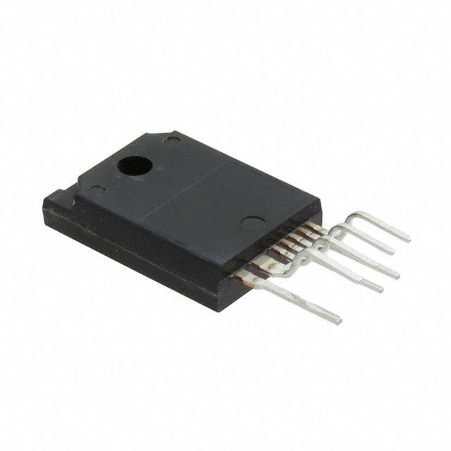
| 描述 | IC FPS PWR SWITCH SMPS TO-220F-4电源开关 IC - 配电 3A/800V 70KHz Power Switch |
| 产品分类 | |
| 品牌 | Fairchild Semiconductor |
| 产品手册 | |
| 产品图片 |
|
| rohs | 符合RoHS无铅 / 符合限制有害物质指令(RoHS)规范要求 |
| 产品系列 | 开关 IC,电源开关 IC - 配电,Fairchild Semiconductor KA5M0380RYDTUFPS™ |
| 数据手册 | |
| 产品型号 | KA5M0380RYDTU |
| 产品 | Power Switches |
| 产品种类 | 电源开关 IC - 配电 |
| 供应商器件封装 | TO-220F-4L |
| 功率(W) | 75W |
| 包装 | 管件 |
| 单位重量 | 2.894 g |
| 商标 | Fairchild Semiconductor |
| 安装风格 | Through Hole |
| 导通电阻—最大值 | 5 Ohms |
| 封装 | Tube |
| 封装/外壳 | TO-220-4 全封装(成形引线) |
| 封装/箱体 | TO-220-4 FP |
| 工作温度 | -40°C ~ 85°C |
| 工作电源电压 | 30 V |
| 工厂包装数量 | 50 |
| 最大功率耗散 | 75 W |
| 最大工作温度 | + 85 C |
| 最小工作温度 | - 40 C |
| 标准包装 | 50 |
| 电压-击穿 | 800V |
| 电压-输入 | 9.6 V ~ 30 V |
| 电压-输出 | - |
| 电流限制 | 2.15 A |
| 电源电流—最大值 | 12 mA |
| 系列 | KA5M0380 |
| 输出电流 | 3 A |
| 输出端数量 | 2 |
| 输出隔离 | 非隔离 |
| 频率范围 | 61kHz ~ 73kHz |


- 商务部:美国ITC正式对集成电路等产品启动337调查
- 曝三星4nm工艺存在良率问题 高通将骁龙8 Gen1或转产台积电
- 太阳诱电将投资9.5亿元在常州建新厂生产MLCC 预计2023年完工
- 英特尔发布欧洲新工厂建设计划 深化IDM 2.0 战略
- 台积电先进制程称霸业界 有大客户加持明年业绩稳了
- 达到5530亿美元!SIA预计今年全球半导体销售额将创下新高
- 英特尔拟将自动驾驶子公司Mobileye上市 估值或超500亿美元
- 三星加码芯片和SET,合并消费电子和移动部门,撤换高东真等 CEO
- 三星电子宣布重大人事变动 还合并消费电子和移动部门
- 海关总署:前11个月进口集成电路产品价值2.52万亿元 增长14.8%


PDF Datasheet 数据手册内容提取
Is Now Part of To learn more about ON Semiconductor, please visit our website at www.onsemi.com Please note: As part of the Fairchild Semiconductor integration, some of the Fairchild orderable part numbers will need to change in order to meet ON Semiconductor’s system requirements. Since the ON Semiconductor product management systems do not have the ability to manage part nomenclature that utilizes an underscore (_), the underscore (_) in the Fairchild part numbers will be changed to a dash (-). This document may contain device numbers with an underscore (_). Please check the ON Semiconductor website to verify the updated device numbers. The most current and up-to-date ordering information can be found at www.onsemi.com. Please email any questions regarding the system integration to Fairchild_questions@onsemi.com. ON Semiconductor and the ON Semiconductor logo are trademarks of Semiconductor Components Industries, LLC dba ON Semiconductor or its subsidiaries in the United States and/or other countries. ON Semiconductor owns the rights to a number of patents, trademarks, copyrights, trade secrets, and other intellectual property. A listing of ON Semiconductor’s product/patent coverage may be accessed at www.onsemi.com/site/pdf/Patent-Marking.pdf. ON Semiconductor reserves the right to make changes without further notice to any products herein. ON Semiconductor makes no warranty, representation or guarantee regarding the suitability of its products for any particular purpose, nor does ON Semiconductor assume any liability arising out of the application or use of any product or circuit, and specifically disclaims any and all liability, including without limitation special, consequential or incidental damages. Buyer is responsible for its products and applications using ON Semiconductor products, including compliance with all laws, regulations and safety requirements or standards, regardless of any support or applications information provided by ON Semiconductor. “Typical” parameters which may be provided in ON Semiconductor data sheets and/or specifications can and do vary in different applications and actual performance may vary over time. All operating parameters, including “Typicals” must be validated for each customer application by customer’s technical experts. ON Semiconductor does not convey any license under its patent rights nor the rights of others. ON Semiconductor products are not designed, intended, or authorized for use as a critical component in life support systems or any FDA Class 3 medical devices or medical devices with a same or similar classification in a foreign jurisdiction or any devices intended for implantation in the human body. Should Buyer purchase or use ON Semiconductor products for any such unintended or unauthorized application, Buyer shall indemnify and hold ON Semiconductor and its officers, employees, subsidiaries, affiliates, and distributors harmless against all claims, costs, damages, and expenses, and reasonable attorney fees arising out of, directly or indirectly, any claim of personal injury or death associated with such unintended or unauthorized use, even if such claim alleges that ON Semiconductor was negligent regarding the design or manufacture of the part. ON Semiconductor is an Equal Opportunity/Affirmative Action Employer. This literature is subject to all applicable copyright laws and is not for resale in any manner.
www.fairchildsemi.com KA5x03xx-SERIES KA5H0365R, KA5M0365R, KA5L0365R KA5H0380R, KA5M0380R, KA5L0380R Fairchild Power Switch(FPS) Features Description • Precision Fixed Operating Frequency (100/67/50kHz) The Fairchild Power Switch(FPS) product family is specially • Low Start-up Current(Typ. 100uA) designed for an off-line SMPS with minimal external • Pulse by Pulse Current Limiting components. The Fairchild Power Switch(FPS) consists of a • Over Current Protection high voltage power SenseFET and a current mode PWM IC. • Over Voltage Protection (Min. 25V) Included PWM controller integrates the fixed frequency • Internal Thermal Shutdown Function oscillator, the under voltage lock-out, the leading edge • Under Voltage Lockout blanking, the optimized gate turn-on/turn-off driver, the • Internal High Voltage Sense FET thermal shutdown protection, the over voltage protection, • Auto-Restart Mode and the temperature compensated precision current sources for the loop compensation and the fault protection circuitry. Applications Compared to a discrete MOSFET and a PWM controller or an RCCsolution, a Fairchild Power Switch(FPS) can reduce • SMPS for VCR, SVR, STB, DVD & DVCD the total component count, design size and weight and at the • SMPS for Printer, Facsimile & Scanner same time increase efficiency, productivity, and system • Adaptor for Camcorder reliability. It has a basic platform well suited for the cost effective design in either a flyback converter or a forward converter TO-220F-4L 1 1. GND 2. Drain 3. VCC 4. FB Internal Block Diagram #3 VCC 32V 5V Internal #2 DRAIN Vref bias SFET Good logic OSC 9V S 5μA 1mA R Q #4 FB − 2.5R L.E.B + 1R 0.1V + 7.5V − S #1 GND Q R + Thermal S/D 27V − Power on reset OVER VOLTAGE S/D Rev.1.0.7 ©2003 Fairchild Semiconductor Corporation
KA5X03XX-SERIES Absolute Maximum Ratings (Ta=25°C, unless otherwise specified) Characteristic Symbol Value Unit KA5H0365R, KA5M0365R, KA5L0365R Drain-Gate Voltage (RGS=1MΩ) VDGR 650 V Gate-Source (GND) Voltage VGS ±30 V Drain Current Pulsed (1) IDM 12.0 ADC Continuous Drain Current (TC=25°C) ID 3.0 ADC Continuous Drain Current (TC=100°C) ID 2.4 ADC Single Pulsed Avalanche Energy (2) EAS 358 mJ Maximum Supply Voltage VCC,MAX 30 V Analog Input Voltage Range VFB -0.3 to VSD V PD 75 W Total Power Dissipation Derating 0.6 W/°C Operating Junction Temperature. TJ +150 °C Operating Ambient Temperature. TA -40 to +85 °C Storage Temperature Range. TSTG -55 to +150 °C KA5H0380R, KA5M0380R, KA5L0380R Drain-Gate Voltage (RGS=1MΩ) VDGR 800 V Gate-Source (GND) Voltage VGS ±30 V Drain Current Pulsed (1) IDM 12.0 ADC Continuous Drain Current (TC=25°C) ID 3.0 ADC Continuous Drain Current (TC=100°C) ID 2.1 ADC Single Pulsed Avalanche Energy (2) EAS 95 mJ Maximum Supply Voltage VCC,MAX 30 V Analog Input Voltage Range VFB -0.3 to VSD V PD 75 W Total Power Dissipation Derating 0.6 W/°C Operating Junction Temperature. TJ +150 °C Operating Ambient Temperature. TA -40 to +85 °C Storage Temperature Range. TSTG -55 to +150 °C Note: 1. Repetitive rating: Pulse width limited by maximum junction temperature 2. L = 51mH, starting Tj = 25°C 3. L = 13μH, starting Tj = 25°C 2
KA5X03XX-SERIES Electrical Characteristics (SenseFET Part) (Ta = 25°C unless otherwise specified) Parameter Symbol Condition Min. Typ. Max. Unit KA5H0365R, KA5M0365R, KA5L0365R Drain-Source Breakdown Voltage BVDSS VGS=0V, ID=50μA 650 - - V VDS=Max. Rating, VGS=0V - - 50 μA Zero Gate Voltage Drain Current IDSS VDS=0.8Max. Rating, - - 200 μA VGS=0V, TC=125°C Static Drain-Source on Resistance (Note) RDS(ON) VGS=10V, ID=0.5A - 3.6 4.5 Ω Forward Transconductance (Note) gfs VDS=50V, ID=0.5A 2.0 - - S Input Capacitance Ciss - 720 - VGS=0V, VDS=25V, Output Capacitance Coss - 40 - pF f=1MHz Reverse Transfer Capacitance Crss - 40 - Turn On Delay Time td(on) VDD=0.5BVDSS, ID=1.0A - 150 - (MOSFET switching Rise Time tr - 100 - time is essentially nS Turn Off Delay Time td(off) - 150 - independent of Fall Time tf operating temperature) - 42 - Total Gate Charge VGS=10V, ID=1.0A, Qg - - 34 (Gate-Source+Gate-Drain) VDS=0.5BVDSS (MOSFET switching time is essentially nC Gate-Source Charge Qgs - 7.3 - independent of Gate-Drain (Miller) Charge Qgd operating temperature) - 13.3 - KA5H0380R, KA5M0380R, KA5L0380R Drain-Source Breakdown Voltage BVDSS VGS=0V, ID=50μA 800 - - V VDS=Max. Rating, VGS=0V - - 250 μA Zero Gate Voltage Drain Current IDSS VDS=0.8Max. Rating, - - 1000 μA VGS=0V, TC=125°C Static Drain-Source on Resistance (Note) RDS(ON) VGS=10V, ID=0.5A - 4.0 5.0 Ω Forward Transconductance (Note) gfs VDS=50V, ID=0.5A 1.5 2.5 - S Input Capacitance Ciss - 779 - VGS=0V, VDS=25V, Output Capacitance Coss - 75.6 - pF f=1MHz Reverse Transfer Capacitance Crss - 24.9 - Turn On Delay Time td(on) VDD=0.5BVDSS, ID=1.0A - 40 - (MOSFET switching Rise Time tr - 95 - time is essentially nS Turn Off Delay Time td(off) - 150 - independent of Fall Time tf operating temperature) - 60 - Total Gate Charge VGS=10V, ID=1.0A, Qg - - 34 (Gate-Source+Gate-Drain) VDS=0.5BVDSS (MOSFET switching time is nC Gate-Source Charge Qgs - 7.2 - essentially independent of Gate-Drain (Miller) Charge Qgd operating temperature) - 12.1 - Note: 1. Pulse test: Pulse width ≤ 300μS, duty ≤ 2% 2. 1 S = ---- R 3
KA5X03XX-SERIES Electrical Characteristics (Control Part) (Continued) (Ta = 25°C unless otherwise specified) Characteristic Symbol Test condition Min. Typ. Max. Unit UVLO SECTION Start Threshold Voltage VSTART VFB=GND 14 15 16 V Stop Threshold Voltage VSTOP VFB=GND 8.4 9 9.6 V OSCILLATOR SECTION KA5H0365R Initial Accuracy FOSC 90 100 110 kHz KA5H0380R KA5M0365R Initial Accuracy FOSC 61 67 73 kHz KA5M0380R KA5L0365R Initial Accuracy FOSC 45 50 55 kHz KA5L0380R Frequency Change With Temperature (2) - -25°C≤Ta≤+85°C - ±5 ±10 % KA5H0365R Maximum Duty Cycle Dmax 62 67 72 % KA5H0380R KA5M0365R KA5M0380R Maximum Duty Cycle Dmax 72 77 82 % KA5L0365R KA5L0380R FEEDBACK SECTION Feedback Source Current IFB Ta=25°C, 0V<Vfb<3V 0.7 0.9 1.1 mA Shutdown Feedback Voltage VSD Vfb>6.5V 6.9 7.5 8.1 V Shutdown Delay Current Idelay Ta=25°C, 5V≤Vfb≤VSD 4 5 6 μA REFERENCE SECTION Output Voltage (1) Vref Ta=25°C 4.80 5.00 5.20 V Temperature Stability (1)(2) Vref/ΔT -25°C≤Ta≤+85°C - 0.3 0.6 mV/°C CURRENT LIMIT(SELF-PROTECTION)SECTION Peak Current Limit IOVER Max. inductor current 1.89 2.15 2.41 A PROTECTION SECTION Over Voltage Protection VOVP VCC>24V 25 27 29 V Thermal Shutdown Temperature (Tj) (1) TSD - 140 160 - °C TOTAL STANDBY CURRENT SECTION Start-up Current ISTART VCC=14V - 100 170 μA Operating Supply Current IOP VCC<28 - 7 12 mA (Control Part Only) Note: 1. These parameters, although guaranteed, are not 100% tested in production 2. These parameters, although guaranteed, are tested in EDS(water test) process 4
KA5X03XX-SERIES Typical Performance Characteristics(SenseFET part) (KA5H0365R, KA5M0365R, KA5L0365R) 10 10 VGS Top : 15V 10V 8.0V 7.0V 6.0V A] 5.5V A] ent [ B o t t o m : 45..50VV ent [ Curr 1 Curr 1 150 oC n n ai ai Dr Dr I, D @Notes: I, D 25 oC -25oC @Notes: 12.. 3T0C0 = μ 2s5 P ouClse Test 12.. V30D0S μ =s 3P0uVlse Test 0.1 0.1 1 10 2 4 6 8 10 V , Drain-Source Voltage [V] V , Gate-Source Voltage [V] DS GS Figure 1. Output Characteristics Figure 2. Transfer Characteristics 7 6 ] esistance 45 Vgs=10V Current [A] 1 R , [ΩDS(on)Source On-R 23 Vgs=20V everse Drain 0.1 150 oC 25 oC @Notes : ain- @ Note : Tj=25℃ , RR 12.. V30G0S μ =s 0P uVlse Test Dr 1 ID 00 1 2 3 4 5 0.01 0.4 0.6 0.8 1.0 1.2 I,Drain Current [A] V , Source-Drain Voltage [V] D SD Figure 3. On-Resistance vs. Drain Current Figure 4. Source-Drain Diode Forward Voltage 700 C = C + C (C = shorted) 10 600 Ciossss = Cgdss + Cggdd ds VDS=130V 500 Ciss Crss = Cgd e[V] 8 VDS=320V Capacitance [pF] 234000000 Gate-Source Voltag 46 VDS=520V Coss V,GS 2 100 C @ Note : ID=3.0A rss 0 0 100 101 0 5 10 15 20 25 V , Drain-Source Voltage [V] Q ,Total Gate Charge [nC] DS G Figure 5. Capacitance vs. Drain-Source Voltage Figure 6. Gate Charge vs. Gate-Source Voltage 5
KA5X03XX-SERIES Typical Performance Characteristics (Continued) (KA5H0365R, KA5M0365R, KA5L0365R) 1.2 2.5 2.0 BV, (Normalized)DSSDrain-Source Breakdown Voltage011...901 @ N12o.. tVIeDG s=S : =2 500VμA R, (Normalized)DS(on)Drain-Source On-Resistance 011...505 @ 12N.. oVIDtGe =sS: 1=. 51 0AV 0.8 -50 0 50 100 150 0.0 -50 0 50 100 150 TJ, Junction Temperature [oC] TJ, Junction Temperature [oC] Figure 7. Breakdown Voltage vs. Temperature Figure 8. On-Resistance vs. Temperature 102 Operation in This Area 3.0 A] is Limited by R DS(on) [ t 101 100 μs 10 μs 2.5 n re 1 ms A] rain Cur 100 DC10 ms n Current [ 12..50 I , DD 10-1 @ N1o.t eTs := 25 oC I, DraiD 1.0 C 2. T = 150 oC 0.5 J 3. Single Pulse 10-2 0.0 100 101 102 103 25 50 75 100 125 150 V , Drain-Source Voltage [V] T , Case Temperature [oC] DS C Figure 9. Max. Safe Operating Area Figure 10. Max. Drain Current vs. Case Temperature 100 D=0.5 e s n o p s Re 0.2 @ Notes : ermal 0.1 12.. ZDuθJtCy( tF)a=c1t.o2r5, oDC=/tW /Mtax. Th10-1 1 2 , 0.05 3. TJM-TC=PDM*ZθJC(t) ) t ( 0.02 C ZJθ 0.01 single pulse 10-2 10-5 10-4 10-3 10-2 10-1 100 101 t , Square Wave Pulse Duration [sec] 1 Figure 11. Thermal Response 6
KA5X03XX-SERIES Typical Performance Characteristics (Continued) (KA5H0380R, KA5M0380R, KA5L0380R) 101 101 VGS Top : 15V 10V 8.0V 7.0V I, Drain Current [A]D 100 B o t t o m :6554....0505VVVV @ N12..o 3Tte0Cs0 μ:= s2 5P uolCse Test I, Drain Current [A]D 100 25 oC150 oC -25 oC @ 12N.. oV3t0De0sS μ: =s 3P0u Vlse Test 10-1 100 101 10-12 4 6 8 10 V , Drain-Source Voltage [V] V , Gate-Source Voltage [V] DS GS Figure 1. Output Characteristics Figure 2. Thansfer Characteristics Fig3. On-Resistance vs. Drain Current 8 7 10 Vgs=10V R , [Ω]DS(on)Drain-Source On-Resistance 123456 Vgs=20V @ Note : Tj=25℃ I, Reverse Drain Current [A]DR 1 150 oC 25 oC @ N12..o V3te0Gs0S: μ =s 0 PVulse Test 0 0.1 0 1 2 3 4 0.4 0.6 0.8 1.0 I ,Drain Current V , Source-Drain Voltage [V] D SD Figure 3. On-Resistance vs. Drain Current Figure 4. Source-Drain Diode Forward Voltage 1000 Capacitance [pF] 345678900000000000000 Ciss CCCiorssssss === CCCggdsds ++ CCggdd (Cds = shorted) ate-Source Voltage[V] 14680 VDSV=D6S4=04VV0D0VS=160V G 120000 CCorssss V,GS 2 @ Note : ID=3.0A 0 0 100 101 0 5 10 15 20 25 30 VDS, Drain-Source Voltage [V] QG,Total Gate Charge [nC] Figure 5. Capacitance vs. Drain-Source Voltage Figure 6. Gate Charge vs. Gate-Source Voltage 7
KA5X03XX-SERIES Typical Performance Characteristics (Continued) (KA5H0380R, KA5M0380R, KA5L0380R) 1.2 2.5 2.0 BV, (Normalized)DSSDrain-Source Breakdown Voltage 011...901 @ N12o.. tVIeDG s=S : =2 500VμA R, (Normalized)DS(on)Drain-Source On-Resistance 011...505 @ 12N..o VItDeG =sS: =1 .150 AV 0.8 0.0 -50 0 50 100 150 -50 0 50 100 150 TJ, Junction Temperature [oC] TJ, Junction Temperature [oC] Figure 7. Breakdown Voltage vs. Temperature Figure 8. On-Resistance vs. Temperature 102 3.5 Operation in This Area [A] is Limited by R DS(on) 3.0 Current 101 1 ms100 μs 10 μs ent [A] 22..05 in 100 DC10 ms Curr , Dra Drain 1.5 I D 10-1 @ N1o.t eTsC := 25 oC I, D 1.0 2. TJ = 150 oC 0.5 3. Single Pulse 10-2 0.0 101 102 103 40 60 80 100 120 140 VDS , Drain-Source Voltage [V] TC, Case Temperature [oC] Figure 9. Max. Safe Operating Area Figure 10. Max. Drain Current vs. Case Temperature 100 D=0.5 (t) , Thermal Response 10-1 0000....021025 @ N123o...t eZDTsuθJJ tMC:y-( TtFC)a==cP1tD.oM2r*5,Z θoJDCC=/(tWt1 )/Mta2x. ZJCθ 0.01 single pulse 10-2 10-5 10-4 10-3 10-2 10-1 100 101 t , Square Wave Pulse Duration [sec] 1 Figure 11. Thermal Response 8
KA5X03XX-SERIES Typical Performance Characteristics (Control Part) (Continued) (These characteristic graphs are normalized at Ta = 25°C) 1.20 1.20 1.15 1.15 1.10 1.10 1.05 1.05 Fosc 1.00 Ifb1.00 0.95 0.95 0.90 0.90 0.85 0.85 0.80 0.80 -40 -25 0 25 50 75 100 125 150 -40 -25 0 25 50 75 100 125 150 Temperature [℃] Temperature [℃] Figure 1. Operating Frequency Figure 2. Feedback Source Current 1.20 1.50 1.15 1.40 1.10 1.30 1.05 1.20 Iop1.00 Iover1.10 0.95 1.00 0.90 0.90 0.85 0.80 0.80 0.70 -40 -25 0 25 50 75 100 125 150 -40 -25 0 25 50 75 100 125 150 Temperature [℃] Temperature [℃] Figure 3. Operating Supply Current Figure 4. Peak Current Limit 1.30 1.20 1.20 1.15 1.10 1.10 1.05 1.00 Istart Vstart1.00 0.90 0.95 0.80 0.90 0.70 0.85 0.60 0.80 -40 -25 0 25 50 75 100 125 150 -40 -25 0 25 50 75 100 125 150 Temperature [℃] Temperature [℃] Figure 5. Start up Current Figure 6. Start Threshold Voltage 9
KA5X03XX-SERIES Typical Performance Characteristics (Continued) (These characteristic graphs are normalized at Ta = 25°C) 1.20 1.20 1.15 1.15 1.10 1.10 1.05 1.05 Vstop1.00 Dmax1.00 0.95 0.95 0.90 0.90 0.85 0.85 0.80 0.80 -40 -25 0 25 50 75 100 125 150 -40 -25 0 25 50 75 100 125 150 Temperature [℃] Temperature [℃] Figure 7. Stop Threshold Voltage Figure 8. Maximum Duty Cycle 1.20 1.20 1.15 1.15 1.10 1.10 1.05 1.05 Vz1.00 Vsd1.00 0.95 0.95 0.90 0.90 0.85 0.85 0.80 0.80 -40 -25 0 25 50 75 100 125 150 -40 -25 0 25 50 75 100 125 150 Temperature [℃] Temperature [℃] Figure 9. VCC Zener Voltage Figure 10. Shutdown Feedback Voltage 1.20 1.20 1.15 1.15 1.10 1.10 1.05 1.05 Idelay1.00 Vovp1.00 0.95 0.95 0.90 0.90 0.85 0.85 0.80 0.80 -40 -25 0 25 50 75 100 125 150 -40 -25 0 25 50 75 100 125 150 Temperature [℃] Temperature [℃] Figure 11. Shutdown Delay Current Figure 12. Over Voltage Protection 10
KA5X03XX-SERIES Typical Performance Characteristics (Continued) (These characteristic graphs are normalized at Ta = 25°C) 3.00 2.50 2.00 Rds(on)1.50 1.00 0.50 0.00 -40 -25 0 25 50 75 100 125 150 Temperature [℃] Figure13. Static Drain-Source on Resistance 11
KA5X03XX-SERIES Package Dimensions TO-220F-4L 12
KA5X03XX-SERIES Package Dimensions (Continued) TO-220F-4L(Forming) 13
KA5X03XX-SERIES Ordering Information Product Number Package Marking Code BVDSS FOSC RDS(on) KA5H0365RTU TO-220F-4L 5H0365R 650V 100kHz 3.6Ω KA5H0365RYDTU TO-220F-4L(Forming) KA5M0365RTU TO-220F-4L 5M0365R 650V 67kHz 3.6Ω KA5M0365RYDTU TO-220F-4L(Forming) KA5L0365RTU TO-220F-4L 5L0365R 650V 50kHz 3.6Ω KA5L0365RYDTU TO-220F-4L(Forming) Product Number Package Marking Code BVDSS FOSC RDS(on) KA5H0380RTU TO-220F-4L 5H0380R 800V 100kHz 4.6Ω KA5H0380RYDTU TO-220F-4L(Forming) KA5M0380RTU TO-220F-4L 5M0380R 800V 67kHz 4.6Ω KA5M0380RYDTU TO-220F-4L(Forming) KA5L0380RTU TO-220F-4L 5L0380R 800V 50kHz 4.6Ω KA5L0380RYDTU TO-220F-4L(Forming) TU :Non Forming Type YDTU : Forming type DISCLAIMER FAIRCHILD SEMICONDUCTOR RESERVES THE RIGHT TO MAKE CHANGES WITHOUT FURTHER NOTICE TO ANY PRODUCTS HEREIN TO IMPROVE RELIABILITY, FUNCTION OR DESIGN. FAIRCHILD DOES NOT ASSUME ANY LIABILITY ARISING OUT OF THE APPLICATION OR USE OF ANY PRODUCT OR CIRCUIT DESCRIBED HEREIN; NEITHER DOES IT CONVEY ANY LICENSE UNDER ITS PATENT RIGHTS, NOR THE RIGHTS OF OTHERS. LIFE SUPPORT POLICY FAIRCHILD’S PRODUCTS ARE NOT AUTHORIZED FOR USE AS CRITICAL COMPONENTS IN LIFE SUPPORT DEVICES OR SYSTEMS WITHOUT THE EXPRESS WRITTEN APPROVAL OF THE PRESIDENT OF FAIRCHILD SEMICONDUCTOR CORPORATION. As used herein: 1. Life support devices or systems are devices or systems 2. A critical component in any component of a life support which, (a) are intended for surgical implant into the body, device or system whose failure to perform can be or (b) support or sustain life, and (c) whose failure to reasonably expected to cause the failure of the life support perform when properly used in accordance with device or system, or to affect its safety or effectiveness. instructions for use provided in the labeling, can be reasonably expected to result in a significant injury of the user. www.fairchildsemi.com 6/3/08 0.0m 001 Stock#DSxxxxxxxx © 2003 Fairchild Semiconductor Corporation
TRADEMARKS The following includes registered and unregistered trademarks and service marks, owned by Fairchild Semiconductor and/or its global subsidiaries, and is not intended to be an exhaustive list of all such trademarks. 2Cool FPS PDP SPM The Power Franchise® AccuPower F-PFS Power-SPM Auto-SPM FRFET® PowerTrench® AX-CAP* Global Power ResourceSM PowerXS™ TinyBoost BitSiC® Green FPS Programmable Active Droop Build it Now Green FPS e-Series QFET® TinyBuck TinyCalc CorePLUS Gmax QS TinyLogic® CorePOWER GTO Quiet Series TINYOPTO CROSSVOLT IntelliMAX RapidConfigure TinyPower CTL ISOPLANAR TinyPWM CDEurUreXnPt ETEraDn®s fer Logic Makianngd S Bmeattlel rS™pe akers Sound Louder SSaigvninaglW oiusre wo rld, 1mW/W/kW at a time™ TTirnaynWSiiCre® Dual Cool™ MegaBuck EcoSPARK® MICROCOUPLER SSMmAarRtMT aSxTA RT TTrRiFUaEuClt UDReRteEcNtT ®* EfficientMax MicroFET SPM® SerDes ESBC MicroPak STEALTH Fairc®hi ld® MMiilclerorDPraivke2 SSuuppeerrSFOETT® -3 UHC® MotionMax Fairchild Semiconductor® SuperSOT-6 Ultra FRFET Motion-SPM FACT Quiet Series SuperSOT-8 UniFET FACT® mWSaver SupreMOS® VCX FFAasStTvC® ore OOOPpPtTToOOHPLiTOLAG NICA®R ® SSyynnccF-LEoTck™ VVioslutaaglMePalxus FETBench XS™ FlashWriter®* ®* ® * Trademarks of System General Corporation, used under license by Fairchild Semiconductor. DISCLAIMER FAIRCHILD SEMICONDUCTOR RESERVES THE RIGHT TO MAKE CHANGES WITHOUT FURTHER NOTICE TO ANY PRODUCTS HEREIN TO IMPROVE RELIABILITY, FUNCTION, OR DESIGN. FAIRCHILD DOES NOT ASSUME ANY LIABILITY ARISING OUT OF THE APPLICATION OR USE OF ANY PRODUCT OR CIRCUIT DESCRIBED HEREIN; NEITHER DOES IT CONVEY ANY LICENSE UNDER ITS PATENT RIGHTS, NOR THE RIGHTS OF OTHERS. THESE SPECIFICATIONS DO NOT EXPAND THE TERMS OF FAIRCHILD’S WORLDWIDE TERMS AND CONDITIONS, SPECIFICALLY THE WARRANTY THEREIN, WHICH COVERS THESE PRODUCTS. LIFE SUPPORT POLICY FAIRCHILD’S PRODUCTS ARE NOT AUTHORIZED FOR USE AS CRITICAL COMPONENTS IN LIFE SUPPORT DEVICES OR SYSTEMS WITHOUT THE EXPRESS WRITTEN APPROVAL OF FAIRCHILD SEMICONDUCTOR CORPORATION. As used herein: 1. Life support devices or systems are devices or systems which, (a) 2. A critical component in any component of a life support, device, or are intended for surgical implant into the body or (b) support or system whose failure to perform can be reasonably expected to sustain life, and (c) whose failure to perform when properly used in cause the failure of the life support device or system, or to affect its accordance with instructions for use provided in the labeling, can be safety or effectiveness. reasonably expected to result in a significant injury of the user. ANTI-COUNTERFEITING POLICY Fairchild Semiconductor Corporation's Anti-Counterfeiting Policy. Fairchild's Anti-Counterfeiting Policy is also stated on our external website, www.fairchildsemi.com, under Sales Support. Counterfeiting of semiconductor parts is a growing problem in the industry. All manufacturers of semiconductor products are experiencing counterfeiting of their parts. Customers who inadvertently purchase counterfeit parts experience many problems such as loss of brand reputation, substandard performance, failed applications, and increased cost of production and manufacturing delays. Fairchild is taking strong measures to protect ourselves and our customers from the proliferation of counterfeit parts. Fairchild strongly encourages customers to purchase Fairchild parts either directly from Fairchild or from Authorized Fairchild Distributors who are listed by country on our web page cited above. Products customers buy either from Fairchild directly or from Authorized Fairchild Distributors are genuine parts, have full traceability, meet Fairchild's quality standards for handling and storage and provide access to Fairchild's full range of up-to-date technical and product information. Fairchild and our Authorized Distributors will stand behind all warranties and will appropriately address any warranty issues that may arise. Fairchild will not provide any warranty coverage or other assistance for parts bought from Unauthorized Sources. Fairchild is committed to combat this global problem and encourage our customers to do their part in stopping this practice by buying direct or from authorized distributors. PRODUCT STATUS DEFINITIONS Definition of Terms Datasheet Identification Product Status Definition Datasheet contains the design specifications for product development. Specifications may change Advance Information Formative / In Design in any manner without notice. Datasheet contains preliminary data; supplementary data will be published at a later date. Fairchild Preliminary First Production Semiconductor reserves the right to make changes at any time without notice to improve design. Datasheet contains final specifications. Fairchild Semiconductor reserves the right to make No Identification Needed Full Production changes at any time without notice to improve the design. Datasheet contains specifications on a product that is discontinued by Fairchild Semiconductor. Obsolete Not In Production The datasheet is for reference information only. Rev. I57 © Fairchild Semiconductor Corporation www.fairchildsemi.com
ON Semiconductor and are trademarks of Semiconductor Components Industries, LLC dba ON Semiconductor or its subsidiaries in the United States and/or other countries. ON Semiconductor owns the rights to a number of patents, trademarks, copyrights, trade secrets, and other intellectual property. A listing of ON Semiconductor’s product/patent coverage may be accessed at www.onsemi.com/site/pdf/Patent−Marking.pdf. ON Semiconductor reserves the right to make changes without further notice to any products herein. ON Semiconductor makes no warranty, representation or guarantee regarding the suitability of its products for any particular purpose, nor does ON Semiconductor assume any liability arising out of the application or use of any product or circuit, and specifically disclaims any and all liability, including without limitation special, consequential or incidental damages. Buyer is responsible for its products and applications using ON Semiconductor products, including compliance with all laws, regulations and safety requirements or standards, regardless of any support or applications information provided by ON Semiconductor. “Typical” parameters which may be provided in ON Semiconductor data sheets and/or specifications can and do vary in different applications and actual performance may vary over time. All operating parameters, including “Typicals” must be validated for each customer application by customer’s technical experts. ON Semiconductor does not convey any license under its patent rights nor the rights of others. ON Semiconductor products are not designed, intended, or authorized for use as a critical component in life support systems or any FDA Class 3 medical devices or medical devices with a same or similar classification in a foreign jurisdiction or any devices intended for implantation in the human body. Should Buyer purchase or use ON Semiconductor products for any such unintended or unauthorized application, Buyer shall indemnify and hold ON Semiconductor and its officers, employees, subsidiaries, affiliates, and distributors harmless against all claims, costs, damages, and expenses, and reasonable attorney fees arising out of, directly or indirectly, any claim of personal injury or death associated with such unintended or unauthorized use, even if such claim alleges that ON Semiconductor was negligent regarding the design or manufacture of the part. ON Semiconductor is an Equal Opportunity/Affirmative Action Employer. This literature is subject to all applicable copyright laws and is not for resale in any manner. PUBLICATION ORDERING INFORMATION LITERATURE FULFILLMENT: N. American Technical Support: 800−282−9855 Toll Free ON Semiconductor Website: www.onsemi.com Literature Distribution Center for ON Semiconductor USA/Canada 19521 E. 32nd Pkwy, Aurora, Colorado 80011 USA Europe, Middle East and Africa Technical Support: Order Literature: http://www.onsemi.com/orderlit Phone: 303−675−2175 or 800−344−3860 Toll Free USA/Canada Phone: 421 33 790 2910 Fax: 303−675−2176 or 800−344−3867 Toll Free USA/Canada Japan Customer Focus Center For additional information, please contact your local Email: orderlit@onsemi.com Phone: 81−3−5817−1050 Sales Representative © Semiconductor Components Industries, LLC www.onsemi.com www.onsemi.com 1
Mouser Electronics Authorized Distributor Click to View Pricing, Inventory, Delivery & Lifecycle Information: O N Semiconductor: KA5M0380RTU KA5M0380RYDTU