ICGOO在线商城 > 集成电路(IC) > PMIC - AC-DC 转换器,离线开关 > NCP1230D100R2G

 Datasheet下载
- 型号: NCP1230D100R2G
- 制造商: ON Semiconductor
- 库位|库存: xxxx|xxxx
- 要求:
| 数量阶梯 | 香港交货 | 国内含税 |
| +xxxx | $xxxx | ¥xxxx |
查看当月历史价格
查看今年历史价格
NCP1230D100R2G产品简介:
ICGOO电子元器件商城为您提供NCP1230D100R2G由ON Semiconductor设计生产,在icgoo商城现货销售,并且可以通过原厂、代理商等渠道进行代购。 NCP1230D100R2G价格参考。ON SemiconductorNCP1230D100R2G封装/规格:PMIC - AC-DC 转换器,离线开关, Converter Offline Flyback Topology 100kHz 8-SOIC。您可以下载NCP1230D100R2G参考资料、Datasheet数据手册功能说明书,资料中有NCP1230D100R2G 详细功能的应用电路图电压和使用方法及教程。
NCP1230D100R2G 是安森美半导体(ON Semiconductor)推出的一款高性能电流模式PWM控制器,常用于AC-DC转换器和离线开关电源设计中。其应用场景主要包括:

1. 电源适配器:适用于笔记本电脑、平板、智能手机等设备的充电器或电源适配器,具备高效率与小体积特性。

2. 消费电子产品电源:如电视、机顶盒、音响系统等家用电器中的内置电源模块。

3. 工业电源系统:用于工业自动化设备、仪表、小型电机驱动等对电源稳定性和可靠性要求较高的场合。

4. LED照明电源:可应用于LED路灯、商业照明等需要恒定直流输出的照明系统中。

5. 电池充电系统:如电动工具、UPS不间断电源等设备中的充电电路部分。

该器件支持宽输入电压范围,具备软启动、过载保护、过压保护等功能,提高了系统的安全性与稳定性,适合多种中低功率离线式开关电源应用。
| 参数 | 数值 |
| 产品目录 | 集成电路 (IC) |
| 描述 | IC CTLR PWM SMPS 100KHZ 8-SOIC |
| 产品分类 | |
| 品牌 | ON Semiconductor |
| 数据手册 | |
| 产品图片 |
|
| 产品型号 | NCP1230D100R2G |
| rohs | 无铅 / 符合限制有害物质指令(RoHS)规范要求 |
| 产品系列 | - |
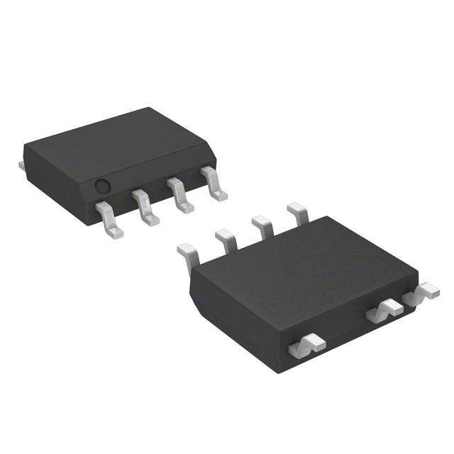
| 供应商器件封装 | 8-SOIC N |
| 其它名称 | NCP1230D100R2GOSCT |
| 功率(W) | - |
| 包装 | 剪切带 (CT) |
| 封装/外壳 | 8-SOIC(0.154",3.90mm 宽) |
| 工作温度 | -40°C ~ 125°C |
| 标准包装 | 1 |
| 电压-击穿 | - |
| 电压-输入 | 8.4 V ~ 18 V |
| 电压-输出 | - |
| 输出隔离 | 隔离 |
| 频率范围 | 100kHz |


- 商务部:美国ITC正式对集成电路等产品启动337调查
- 曝三星4nm工艺存在良率问题 高通将骁龙8 Gen1或转产台积电
- 太阳诱电将投资9.5亿元在常州建新厂生产MLCC 预计2023年完工
- 英特尔发布欧洲新工厂建设计划 深化IDM 2.0 战略
- 台积电先进制程称霸业界 有大客户加持明年业绩稳了
- 达到5530亿美元!SIA预计今年全球半导体销售额将创下新高
- 英特尔拟将自动驾驶子公司Mobileye上市 估值或超500亿美元
- 三星加码芯片和SET,合并消费电子和移动部门,撤换高东真等 CEO
- 三星电子宣布重大人事变动 还合并消费电子和移动部门
- 海关总署:前11个月进口集成电路产品价值2.52万亿元 增长14.8%


PDF Datasheet 数据手册内容提取
NCP1230 Low-Standby Power High Performance PWM Controller The NCP1230 represents a major leap towards achieving low standby power in medium−to−high power Switched−Mode Power www.onsemi.com Supplies such as notebook adapters, off−line battery chargers and consumer electronics equipment. Housed in a compact 8−pin package MARKING (SOIC−8, SOIC−7, or PDIP−7), the NCP1230 contains all needed DIAGRAM control functionality to build a rugged and efficient power supply. The NCP1230 is a current mode controller with internal ramp 8 compensation. Among the unique features offered by the NCP1230 is SOIC−8 VHVIC 230Dy an event management scheme that can disable the front−end PFC D SUFFIX ALYWy 8 CASE 751 (cid:2) circuit during standby, thus reducing the no load power consumption. 1 1 The NCP1230 itself goes into cycle skipping at light loads while limiting peak current (to 25% of nominal peak) so that no acoustic noise is generated. The NCP1230 has a high−voltage startup circuit 8 that eliminates external components and reduces power consumption. SOIC−7 8 30D16 The NCP1230 also features an internal latching function that can be D1 SUFFIX ALYW(cid:2) used for OVP protection. This latch is triggered by pulling the CS pin 1 CASE 751U (cid:2) above 3.0 V and can only be reset by pulling VCC to ground. True 1 overload protection, internal 2.5 ms soft−start, internal leading edge blanking, internal frequency dithering for low EMI are some of the other important features offered by the NCP1230. PDIP−7 VHVIC 1230Pxxx P SUFFIX AWL Features 8 CASE 626B YYWWG • Current−Mode Operation with Internal Ramp Compensation 1 1 • Internal High−Voltage Startup Current Source for Loss−Less Startup • Extremely Low No−Load Standby Power xxx = Device Code: 65, 100, 133 • y = Device Code: 6, 1, 1 Skip−Cycle Capability at Low Peak Currents y = Device Code: 5, 0, 3 • Direct Connection to PFC Controller for Improved No−Load Standby A = Assembly Location Power L = Wafer Lot • Y, YY = Year Internal 2.5 ms Soft−Start W, WW = Work Week • Internal Leading Edge Blanking G = Pb−Free Package • (cid:2) = Pb−Free Package Latched Primary Overcurrent and Overvoltage Protection (Note: Microdot may be in either location) • Short−Circuit Protection Independent of Auxiliary Level • Internal Frequency Jittering for Improved EMI Signature • +500 mA/−800 mA Peak Current Drive Capability PIN CONNECTIONS • Available in Three Frequency Options: 65 kHz, 100 kHz, and 133 kHz 1 8 • PFC Vcc HV Direct Optocoupler Connection FB • SPICE Models Available for TRANsient and AC Analysis CS VCC • This is a Pb−Free Device GND DRV Typical Applications • High Power AC−DC Adapters for Notebooks, etc. • ORDERING INFORMATION Offline Battery Chargers • See detailed ordering and shipping information in the ordering Set−Top Boxes Power Supplies, TV, Monitors, etc. information section on page 4 of this data sheet. © Semiconductor Components Industries, LLC, 2015 1 Publication Order Number: May, 2015 − Rev. 12 NCP1230/D
NCP1230 HV + Vout PFC_VCC 1 8 1 8 OVP OVP GN- 2 7 2 7 D + 3 6 3 6 CBulk 4 5 4 5 NCP1230 MC33262/33260 Ramp Comp Rsense VCC Cap 10 k GND Figure 1. Typical Application Example PIN FUNCTION DESCRIPTION Pin No. Pin Name Function Pin Description 1 PFC VCC This pin provides This pin is a direct connection to the VCC pin (Pin 6) via a low impedance switch. In the bias voltage to standby and during the startup sequence, the switch is open and the PFC VCC is the PFC controller. shut down. As soon as the aux. winding is stabilized, Pin 1 connects to the VCC pin and provides bias to the PFC controller. It goes down in standby and fault conditions. 2 FB Feedback Signal An optocoupler collector pulls this pin low to regulate. When the current setpoint reaches 25% of the maximum peak, the controller skips cycles. 3 CS/OVP Current Sense This pin incorporates three different functions: the current sense function, an internal ramp compensation signal and a 3.0 V latch−off level which latches the output off until VCC is recycled. 4 GND IC Ground − 5 DRV Driver Output With a drive capability of +500 mA / −800 mA, the NCP1230 can drive large Qg MOSFETs. 6 VCC VCC Input The controller accepts voltages up to 18 V and features a UVLO turn−off threshold of 7.7 V typical. 7 NC − − 8 HV High−Voltage This pin connects to the bulk voltage and offers a lossless startup sequence. The charging current is high enough to support the bias needs of a PWM controller through Pin 1. www.onsemi.com 2
NCP1230 8 6 5 HV mAdc VCC DRV 2 3. V 0 2 VVV Vcc MgmtVccoff=12.6Vccmin=7.7Vcclatch=5.6 InternalBias / 2 Vcomp + − 0 Vdc QR S 4 4. p pp Vm eset C 2.3 Ra ccr OS V yn co enati malown FrequModul TherShutd secmer Q 5 mS Ti R S 2.S Off − h c M at W L P − + + − c Vc ult Skip FC_ Fa c P Vdc Vdd V max) 3.0 Vd + − − + 1.25 mp (1 a R art c St d − 75 V + − Soft 0. 1 _Vcc msecmer Error SW FC 25 Ti 5k 25k B P 1 5 E c d_fb 18k L 10 V PFC_Vc Vd 20k B 10 V S ND F C G 1 2 3 4 Figure 2. Internal Circuit Architecture www.onsemi.com 3
NCP1230 MAXIMUM RATINGS (Notes 1 and 2) Rating Symbol Value Unit Maximum Voltage on Pin 8 VDS −0.3 to 500 V Maximum Current IC2 100 mA Power Supply Voltage, Pin 6 VCC −0.3 to 18 V Current ICC2 100 mA Drive Output Voltage, Pin 5 VDV 18 V Drive Current Io 1.0 A Voltage Current Sense Pin, Pin 3 Vcs 10 V Current Ics 100 mA Voltage Feedback, Pin 2 Vfb 10 V Current Ifb 100 mA Voltage, Pin 1 VPFC 18 V Maximum Continuous Current Flowing from Pin 1 IPFC 35 mA Thermal Resistance, Junction−to−Air, PDIP Version R(cid:2)JA 100 °C/W Thermal Resistance, Junction−to−Air, SOIC Version R(cid:2)JA 178 °C/W Maximum Power Dissipation @ TA = 25°C PDIP Pmax 1.25 W SOIC 0.702 Maximum Junction Temperature TJ 150 °C Storage Temperature Range Tstg −60 to +150 °C Stresses exceeding those listed in the Maximum Ratings table may damage the device. If any of these limits are exceeded, device functionality should not be assumed, damage may occur and reliability may be affected. 1. This device series contains ESD protection and exceeds the following tests: Pin 1−6:Human Body Model 2000 V per JEDEC Standard JES22, Method A114E. Machine Model Method 200 V per JEDEC Standard JESD22, Method A115A. Pin 8 is the HV startup of the device and is rated to the maximum rating of the part, or 500 V. 2. This device contains latchup protection and exceeds 100 mA per JEDEC Standard JESD78. ORDERING INFORMATION Device Package Shipping† NCP1230D165R2G SOIC−7 2500 / Tape & Reel (Pb−Free) NCP1230D65R2G SOIC−8 2500 / Tape & Reel (Pb−Free) NCP1230D100R2G SOIC−8 2500 / Tape & Reel (Pb−Free) NCP1230D133R2G SOIC−8 2500 / Tape & Reel (Pb−Free) NCP1230P65G PDIP−7 50 Units/ Rail (Pb−Free) NCP1230P100G PDIP−7 50 Units/ Rail (Pb−Free) NCP1230P133G PDIP−7 50 Units/ Rail (Pb−Free) †For information on tape and reel specifications, including part orientation and tape sizes, please refer to our Tape and Reel Packaging Specifications Brochure, BRD8011/D. www.onsemi.com 4
NCP1230 ELECTRICAL CHARACTERISTICS (For typical values TJ = 25°C, for min/max values TJ = −40°C to +125°C, Max TJ = 150°C, VCC = 13 V, VPIN8 = 30 V unless otherwise noted.) Characteristic Symbol Pin Min Typ Max Unit Supply Section (All frequency versions, otherwise noted) Turn−On Threshold Level, VCC Going Up (Vfb = 2.0 V) VCCOFF 6 11.6 12.6 13.6 V Minimum Operating Voltage after Turn−On VCC(min) 6 7.0 7.7 8.4 V VCC Decreasing Level at which the Latch−Off Phase Ends (Vfb = 3.5 V) VCClatch 6 5.0 5.6 6.2 V VCC Level at which the Internal Logic gets Reset VCCreset 6 − 4.0 − V Internal IC Consumption, No Output Load on Pin 6 (Vfb = 2.5 V) ICC1 6 0.6 1.1 1.8 mA Internal IC Consumption, 1.0 nF Output Load on Pin 6, FSW = 65 kHz ICC2 6 1.3 1.8 2.5 mA (Vfb = 2.5 V) Internal IC Consumption, 1.0 nF Output Load on Pin 6, FSW = 100 kHz ICC2 6 1.3 2.2 3.0 mA Internal IC Consumption, 1.0 nF Output Load on Pin 6, FSW = 133 kHz ICC2 6 1.3 2.8 3.3 mA Internal IC Consumption, Latch−Off Phase ICC3 6 400 680 1000 (cid:3)A Internal Startup Current Source High−Voltage Current Source, 1.0 nF Load IC1 8 1.8 3.2 4.2 mA (VCCOFF −0.2 V, Vfb = 2.5 V, VPIN8 = 30 V) High−Voltage Current Source (VCC = 0 V) IC2 8 1.8 4.4 5.6 mA Minimum Startup Voltage (Ic = 0.5 mA, VCCOFF −0.2 V, Vfb = 2.5 V) VHVmin 8 − 20 23 V Startup Leakage (VPIN8 = 500 V) IHVLeak 8 10 30 80 (cid:3)A Drive Output Output Voltage Rise−Time @ CL = 1.0 nF, 10−90% of Output Signal Tr 5 − 40 − ns Output Voltage Fall−Time @ CL = 1.0 nF, 10−90% of Output Signal Tf 5 − 15 − ns Source Resistance, RLoad 300 (cid:4) (Vfb = 2.5 V) ROH 5 6.0 12.3 25 (cid:4) Sink Resistance, at 1.0 V on Pin 5 (Vfb = 3.5 V) ROL 5 3.0 7.5 18 (cid:4) Pin 1 Output Impedance (or Rdson between Pin 1 and Pin 6 when SW1 RPFC 1 6.0 11.7 23 (cid:4) is closed) Rload on Pin 1 = 680 (cid:4) Current Comparator and Thermal Shutdown Input Bias Current @ 1.0 V Input Level on Pin 3 IIB 3 − 0.02 − (cid:3)A Maximum Internal Current Setpoint Tj = 25°C ILimit 3 1.010 1.063 1.116 V Tj = −40°C to +125°C 0.979 − 1.127 Default Internal Setpoint for Skip Cycle Operation and Standby Vskip 3 600 750 900 mV Detection Default Internal Setpoint to Leave Standby Vstby−out − 1.0 1.25 1.5 V Propagation Delay from CS Detected to Gate Turned Off (VGate = 10 V) TDEL CS 3 − 90 180 ns (Pin 5 Loaded by 1.0 nF) Leading Edge Blanking Duration TLEB 3 100 200 350 ns Soft−Start Period (Note 3) SS − − 2.5 − ms Temperature Shutdown, Maximum Value (Note 3) TSD − 150 165 − °C Hysteresis while in Temperature Shutdown (Note 3) TSD hyste − − 25 − °C Product parametric performance is indicated in the Electrical Characteristics for the listed test conditions, unless otherwise noted. Product performance may not be indicated by the Electrical Characteristics if operated under different conditions. 3. Verified by Design. www.onsemi.com 5
NCP1230 ELECTRICAL CHARACTERISTICS (For typical values TJ = 25°C, for min/max values TJ = −40°C to +125°C, Max TJ = 150°C, VCC = 13 V, VPIN8 = 30 V unless otherwise noted.) Characteristic Symbol Pin Min Typ Max Unit Internal Oscillator Oscillation Frequency, 65 kHz Version (Vfb = 2.5 V) Tj = 25°C fOSC − 60 65 70 kHz Tj = 0°C to +125°C 58 − 72 Tj = −40°C to +125°C 55 − 72 Oscillation Frequency, 100 kHz Version Tj = 25°C fOSC − 93 100 107 kHz Tj = 0°C to +125°C 90 − 110 Tj = −40°C to +125°C 85 − 110 Oscillation Frequency, 133 kHz Version Tj = 25°C fOSC − 123 133 143 kHz Tj = 0°C to +125°C 120 − 146 Tj = −40°C to +125°C 113 − 146 Internal Modulation Swing, in Percentage of Fsw (Vfb = 2.5 V) (Note 4) − − − (cid:2)6.4 − % Internal Swing Period (Note 4) − − − 5.0 − ms Maximum Duty−Cycle (CS = 0, Vfb = 2.5 V) Dmax − 75 80 85 % Internal Ramp Compensation Internal Resistor (Note 4) Rup 3 9.0 18 36 k(cid:4) Ramp Compensation Sawtooth Amplitude − 3 − 2.3 − Vpp Feedback Section Opto Current Source (Vfb = 0.75 V) − 2 200 235 270 (cid:3)A Pin 3 to Current Setpoint Division Ratio (Note 4) Iratio − − 2.8 − − Protection Timeout before Validating Short−Circuit or PFC VCC (Note 4) TDEL − − 125 − ms Latch−Off Level Vlatch 3 2.7 3.0 3.3 V Product parametric performance is indicated in the Electrical Characteristics for the listed test conditions, unless otherwise noted. Product performance may not be indicated by the Electrical Characteristics if operated under different conditions. 4. Verified by Design. TYPICAL PERFORMANCE CHARACTERISTICS 13.0 8.0 VCC = 0 V VPIN8 = 30 V VPIN8 = 30 V V) 12.8 V) 7.8 D ( D ( L L O O H 12.6 H 7.6 S S E E R R H H T 12.4 T 7.4 , off) min) C( C( VC12.2 VC 7.2 12.0 7.0 −50 −25 0 25 50 75 100 125 150 −50 −25 0 25 50 75 100 125 150 TJ, JUNCTION TEMPERATURE (°C) TJ, JUNCTION TEMPERATURE (°C) Figure 3. V Threshold vs. Temperature Figure 4. V Threshold vs. Temperature CC(OFF) CC(min) www.onsemi.com 6
NCP1230 TYPICAL PERFORMANCE CHARACTERISTICS 6.0 1.6 VPIN8 = 30 V VCC = 13 V V) D ( 5.8 1.35 L O H ES 5.6 A) R m TH (1 1.1 H 5.4 CC C I T A L 0.85 CC 5.2 V 5.0 0.6 −50 −25 0 25 50 75 100 125 150 −50 −25 0 25 50 75 100 125 150 TJ, JUNCTION TEMPERATURE (°C) TJ, JUNCTION TEMPERATURE (°C) Figure 5. V Latch Threshold vs. Temperature Figure 6. I Internal Current Consumption, No Load CC CC1 vs. Temperature 3.1 800 133 kHz VCC = 13 V 2.7 700 A) A) m (cid:3) (C2 2.3 100 kHz (C3600 C C I I 1.9 500 65 kHz 1.5 400 −50 −25 0 25 50 75 100 125 150 −50 −25 0 25 50 75 100 125 150 TJ, JUNCTION TEMPERATURE (°C) TJ, JUNCTION TEMPERATURE (°C) Figure 7. I Internal Current Consumption, Figure 8. I Internal Consumption, CC2 CC3 1.0 nF Load vs. Temperature Latch−Off Phase vs. Temperature 4.0 5.0 VCC = VCC − 0.2 V VPIN8 = 30 V VPIN8 = 30 V VCC = 0 V 3.5 4.5 A) A) m m (C1 3.0 (C24.0 I I 2.5 3.5 2.0 3.0 −50 −25 0 25 50 75 100 125 150 −50 −25 0 25 50 75 100 125 150 TJ, JUNCTION TEMPERATURE (°C) TJ, JUNCTION TEMPERATURE (°C) Figure 9. I Startup Current vs. Temperature Figure 10. I Startup Current vs. Temperature C1 C2 www.onsemi.com 7
NCP1230 TYPICAL PERFORMANCE CHARACTERISTICS 22.0 100 VCC = VCC(off) − 0.2 V VCC = 13 V 21.5 A) (cid:3) 75 UM (V) 21.0 RENT ( TJ = −40 °C M R NI 20.5 CU 50 MIHV20.0 AGE TJ = +25 °C V K A 25 E 19.5 L TJ = +125 °C 19.0 0 −50 −25 0 25 50 75 100 125 150 1 10 50 200 400 600 800 850 950 TJ, JUNCTION TEMPERATURE (°C) VDRAIN, VOLTAGE (V) Figure 11. Minimum Startup Voltage vs. Temperature Figure 12. Leakage Current vs. Temperature 18 15 (cid:4)CE () 16 VCC = 13 V (cid:4)E () 1134 VCC = 13 V N C A N 12 SIST 14 STA 11 E SI R E 10 E R C 12 K 9.0 R N SOU E SI 8.0 VE 10 RIV 7.0 RI D 6.0 D 8.0 5.0 −50 −25 0 25 50 75 100 125 150 −50 −25 0 25 50 75 100 125 150 TJ, JUNCTION TEMPERATURE (°C) TJ, JUNCTION TEMPERATURE (°C) Figure 13. Drive Source Resistance vs. Temperature Figure 14. Drive Sink Resistance vs. Temperature 18 1.20 17 VCC = 13 V VCC = 13 V 1.15 (cid:4)) 16 max E ( 15 C 1.10 AN 14 V) RESIST 1123 I (Limit1.05 typ C, 11 1.00 PF min R 10 0.95 9.0 8.0 0.90 −50 −25 0 25 50 75 100 125 150 −50 −25 0 25 50 75 100 125 150 TJ, JUNCTION TEMPERATURE (°C) TJ, JUNCTION TEMPERATURE (°C) Figure 15. RPFC vs. Temperature Figure 16. I vs. Temperature Limit www.onsemi.com 8
NCP1230 TYPICAL PERFORMANCE CHARACTERISTICS 800 1.40 VCC = 13 V VCC = 13 V 1.35 775 1.30 (mV)p 750 (V)−out1.25 Vski stby V 1.20 725 1.15 700 1.10 −50 −25 0 25 50 75 100 125 150 −50 −25 0 25 50 75 100 125 150 TJ, JUNCTION TEMPERATURE (°C) TJ, JUNCTION TEMPERATURE (°C) Figure 17. V vs. Temperature Figure 18. V vs. Temperature skip stby−out 4.0 80 VCC = 13 V 75 3.5 ms) Hz) 70 RT ( 3.0 CY (k TA N 65 S E T− 2.5 QU OF RE 60 S F 2.0 55 1.5 50 −50 −25 0 25 50 75 100 125 150 −50 −25 0 25 50 75 100 125 150 TJ, JUNCTION TEMPERATURE (°C) TJ, JUNCTION TEMPERATURE (°C) Figure 19. Soft−Start vs. Temperature Figure 20. Frequency (65 kHz) vs. Temperature 110 145 VCC = 13 V VCC = 13 V 106 141 z) z) H H k k Y (102 Y (137 C C N N E E U U Q 98 Q133 E E R R F F 94 129 90 125 −50 −25 0 25 50 75 100 125 150 −50 −25 0 25 50 75 100 125 150 TJ, JUNCTION TEMPERATURE (°C) TJ, JUNCTION TEMPERATURE (°C) Figure 21. Frequency (100 kHz) vs. Temperature Figure 22. Frequency (133 kHz) vs. Temperature www.onsemi.com 9
NCP1230 TYPICAL PERFORMANCE CHARACTERISTICS 10.0 81.0 G (%) VCC = 13 V fosc = 65 kHz VCC = 13 V N 9.0 WI %)80.5 N S 8.0 X ( O MA ATI E L 7.0 L80.0 U C D Y O C M 6.0 Y NAL DUT79.5 R 5.0 E T N I 4.0 79.0 −50 −25 0 25 50 75 100 125 150 −50 −25 0 25 50 75 100 125 150 TJ, JUNCTION TEMPERATURE (°C) TJ, JUNCTION TEMPERATURE (°C) Figure 23. Internal Modulation Swing Figure 24. Maximum Duty Cycle vs. Temperature vs. Temperature 280 24 Vfb = 0.75 V VCC = 13 V 270 22 260 20 250 A) (cid:4)) 18 (cid:3) (opto 240 R (kup 16 I 230 14 220 210 12 200 10 −50 −25 0 25 50 75 100 125 150 −50 −25 0 25 50 75 100 125 150 TJ, JUNCTION TEMPERATURE (°C) TJ, JUNCTION TEMPERATURE (°C) Figure 25. I vs. Temperature Figure 26. Internal Ramp Compensation Resistor opto vs. Temperature 150 3.50 s) m 140 Y ( 3.25 A L E TIME D 130 (V)atch3.00 T 120 Vl L U A F L 2.75 E 110 D T 100 2.50 −50 −25 0 25 50 75 100 125 150 −50 −25 0 25 50 75 100 125 150 TJ, JUNCTION TEMPERATURE (°C) TJ, JUNCTION TEMPERATURE (°C) Figure 27. Fault Time Delay vs. Temperature Figure 28. Vl vs. Temperature atch www.onsemi.com 10
NCP1230 OPERATING DESCRIPTION Introduction PFC_V CC The NCP1230 is a current mode controller which provides As shown on the internal NCP1230 diagram, an internal a high level of integration by providing all the required low impedance switch SW1 routes Pin 6 (V ) to Pin 1 CC control logic, protection, and a PWM Drive Output into a when the power supply is operating under nominal load single chip which is ideal for low cost, medium to high conditions. The PFC_V signal is capable of delivering up CC power off−line application, such as notebook adapters, to 35 mA of continuous current for a PFC Controller, or battery chargers, set−boxes, TV, and computer monitors. other logic. The NCP1230 can be connected directly to a high voltage Connecting the NCP1230 PFC_V output to a PFC CC source providing lossless startup, and eliminating external Controller chip is very straight forward, refer to the “Typical startup circuitry. In addition, the NCP1230 has a PFC_V Application Example” all that is generally required is a CC output pin which provides the bias supply power for a Power small decoupling capacitor (0.1 (cid:3)F). Factor Correction controller, or other logic. The NCP1230 has an event management scheme which disables the PFC_V output during standby, and overload conditions. CC High Voltage + Vout PFC_VCC 1 8 1 8 GND 2 7 2 7 3 6 3 6 4 5 4 5 NCP1230 MC33262/33260 Rsense VCC Cap GND Figure 29. Typical Application Example www.onsemi.com 11
NCP1230 FeTehdeb afcekedback pin has been designed to be connected Ipk(cid:3)R0s.7(cid:4)53 directly to the open−collector output of an optocoupler. The where: pin is pulled−up through a 20 k(cid:4) resistor to the internal Vdd_fb supply (5 volts nominal). The feedback input signal Ipk(cid:4)Rs(cid:3)1V (cid:5) is divided down, by a factor of three, and connected to the negative (−) input of the PWM comparator. The positive (+) Ipk(cid:3) 2L(cid:4)pP(cid:4)ifn input to the PWM comparator is the current sense signal (Figure 30). where: The NCP1230 is a peak current mode controller, where P = is the power level where the NCP1230 will go into in the feedback signal is proportional to the output power. At the skip mode the beginning of the cycle, the power switch is turns−on and L = Primary inductance p the current begins to increase in the primary of the f = NCP1230 controller frequency transformer, when the peak current crosses the feedback voltage level, the PWM comparators switches from a logic Pin(cid:3)Lp(cid:4)f(cid:4)Ipk2 2 level low, to a logic level high, resetting the PWM latching Flip−Flop, turning off the power switch until the next Pin(cid:3)Pout Eff oscillator clock cycle begins. where: Vdd_fb Eff = the power supply efficiency Rout(cid:3)Eout2 20k Pout 55k FB 2 − PWM S is rising edge triggered + 10 V 25k R is falling edge triggered Vskip / Vstby−out 2.3 Vpp + 1.25 V + 125 ms Ramp S − R 18k 3 LEB Vdd_fb Figure 30. PFC_VCC FB − The feedback pin input is clamped to a nominal 10 volt for Latch + ESD protection. Reset + Vskip 0.75 V Skip Mode The feedback input is connected in parallel with the skip CS Cmp cycle logic (Figure 31). When the feedback voltage drops below 25% of the maximum peak current (1.0 V/Rsense) the Figure 31. IC prevents the current from decreasing any further and starts to blank the output pulses. This is called the skip cycle During the skip mode the PFC_Vcc signal (pin 1) is mode. While the controller is in the burst mode the power asserted into a high impedance state when a light load transfer now depends upon the duty cycle of the pulse burst condition is detected and confirmed, Figure 32 shows width which reduces the average input power demand. typical waveforms. The first section of the waveform shows Vc(cid:3)Ipk(cid:4)Rs(cid:4)3 a normal startup condition, where the output voltage is low, as a result the feedback signal will be high asking the where: controller to provide the maximum power to the output. The Vc = control voltage (Feedback pin input), second phase is under normal loading, and the output is in Ipk = Peak primary current, regulation. The third phase is when the output power drops Rs = Current sense resistor, below the 25% threshold (the feedback voltage drops to 0.75 3 = Feedback divider ratio. volts). When this occurs, the 125 msec timer starts, and if the SkipLevel(cid:3)3V(cid:4)25%(cid:3)0.75V conditions is still present after the time output period, the www.onsemi.com 12
NCP1230 NCP1230 confirms that the low output power condition is Ramp Compensation present, and the internal SW1 opens, and the PFC_Vcc In Switch Mode Power Supplies operating in Continuous signal output is shuts down. While the NCP1230 is in the Conduction Mode (CCM) with a duty−cycle greater than skip mode the FB pin will move around the 750 mV 50%, oscillation will take place at half the switching threshold level, with approximately 100 mVp−p of frequency. To eliminate this condition, Ramp Compensation hysteresis on the skip comparator, at a period which depends can be added to the current sense signal to cure sub harmonic upon the (light) loading of the power supply and its various oscillations. To lower the current loop gain one typically time constants. Since this ripple amplitude superimposed injects between 50 and 100% of the inductor down slope. over the FB pin is lower than the second threshold (1.25 The NCP1230 provides an internal 2.3 Vpp ramp which volt), the PFC_Vcc comparator output stays high (PFC_Vcc is summed internally through a 18 k(cid:4) resistor to the current output Pin 1 is low). sense pin. To implement ramp compensation a resistor needs In Phase four, the output power demands have increases to be connected from the current sense resistor, to the current and the feedback voltage rises above the 1.25 volts sense pin 3. threshold, the NCP1230 exits the skip mode, and returns to Example: normal operation. If we assume we are using the 65 kHz version of the NCP1230, at 65 kHz the dv/dt of the ramp is 130 mV/(cid:3)s. Assuming we are designing a FLYBACK converter which Max IP has a primary inductance, Lp, of 350 (cid:3)H, and the SMPS has a +12 V output with a Np:Ns ratio of 1:0.1. The OFF time primary current slope is given by: Regulation VFB (Vout(cid:6)Vf)(cid:4)NNps = 371 mA/(cid:3)s or 37 mV/(cid:3)s Skip + 60% 1.25 V Lp 0.75 V when imposed on a current sense resistor (Rsense) of 0.1 (cid:4). If we select 75% of the inductor current downslope as our required amount of ramp compensation, then we shall inject PFC is Off PFC is Off No Delay 27 mV/(cid:3)s. 125 ms With our internal compensation being of 130 mV, the Delay PFC is On PFC is On divider ratio (divratio) between Rcomp and the 18 k(cid:4) is 0.207. Therefore: Figure 32. Rcomp(cid:3)(118(cid:7)k(cid:4)ddivivrraatitoio) = 4.69 k(cid:4) Leaving Standby (Skip Mode) 2.3 V When the feedback voltage rises above the 1.25 volts reference (leaving standby) the skip cycle activity stops and SW1 immediately closes and restarts the PFC, there is no 0V delay in turning on SW1 under these conditions, refer to Figure 32. 18 k Current Sense Rcomp The NCP1230 is a peak current mode controller, where + LEB the current sense input is internally clamped to 1.0 V, so the − CS sense resister is determined by Rsense = 1.0 V /Ipk Rsense maximum. There is a 18k resistor connected to the CS pin, the other Fb/3 end of the 18k resistor is connect to the output of the internal Figure 33. oscillator for ramp compensation (refer to Figure 33). www.onsemi.com 13
NCP1230 Leading Edge Blanking isolated secondary output and on the auxiliary winding. In Switch Mode Power Supplies (SMPS) there can be a Because the auxiliary winding and diode form a peak large current spike at the beginning of the current ramp due rectifier, the auxiliary Vcc capacitor voltage can be charged to the Power Switch gate to source capacitance, transformer up to the peak value rather than the true plateau which is interwinding capacitance, and output rectifier recovery proportional to the output level. time. To prevent prematurely turning off the PWM drive To resolve these issues the NCP1230 monitors the 1.0 V output, a Leading Edges Blanking (LEB) (Figure 34) circuit error flag. As soon as the internal 1.0 V error flag is asserted is place is series with the current sense input, and PWM high, a 125 ms timer starts. If at the end of the 125 ms timeout comparator. The LEB circuit masks the first 250 ns of the period, the error flag is still asserted then the controller current sense signal. determines that there is a true fault condition and stops the PWM drive output, refer to Figure 35. When this occurs, Thermal Shutdown Vcc starts to decrease because the power supply is locked Skip 125 msec Timer out. When Vcc drops below UVLOlow (7.7 V typical), it 2.3 Vpp PWM Comparator enters a latch−off phase where the internal consumption is Ramp FB/3 - reduced down to 680 (cid:3)A (typical). The voltage on the Vcc + Vccreset capacitor continues to drop, but at a lower rate. When Vcc 18 k reaches the latch−off level (5.6 V), the current source is CS R Q 3 LEB + turned on and pulls Vcc above UVLOhigh. To limit the fault 10 V 250 ns - Latch−Off S output power, a divide−by−two circuit is connected to the Vcc pin that requires two startup sequences before 3 V attempting to restart the power supply. If the fault has gone and the error flag is low, the controller resumes normal Figure 34. operations. Under transient load conditions, if the error flag is asserted, the error flag will normally drop prior to the 125 ms Short−Circuit Condition timeout period and the controller continues to operate The NCP1230 is different from other controllers which normally. use an auxiliary windings to detect events on the isolated If the 125 msec timer expires while the NCP1230 is in the secondary output. There maybe some conditions (for Skip Mode, SW1 opens and the PFC_Vcc output will shut example when the leakage inductance is high) where it can down and will not be activated until the fault goes away and be extremely difficult to implement short−circuit and the power supply resumes normal operations. overload protection. This occurs because when the power While in the Skip Mode, to avoid any thermal runaway it switch opens, the leakage inductance superimposes a large is desirable for the Burst duty cycle to be kept below spike on the switch drain voltage. This spike is seen on the 20%(the burst duty−cycle is defined as Tpulse / Tfault). www.onsemi.com 14
NCP1230 12.6V 7.7V 125ms 125ms 125ms 125ms Figure 35. The latch−off phase can also be initiated, more classically, 125 ms time−out, or the error flag before it goes into the when Vcc drops below UVLO (7.7 V typical). During this latch−off phase, operating in the skip mode under these fault detection method, the controller will not wait for the conditions, refer to Figure 36. Regulation Fault Regulation 12.6 V VCC PWM 7.7 V 5.6 V 2.5 ms Timer SS 125 ms 125 ms 1 V Flag PFC VCC Figure 36. www.onsemi.com 15
NCP1230 Current Sense Input Pin Latch−Off Vccoff (12.6 V typically), the current source is turned off The NCP1230 features a fast comparator (Figure 34) that reducing the amount of power being dissipated in the chip. monitors the current sense pin during the controller off time. The NCP1230 then turns on the drive output to the external If for any reason the voltage on pin 3 increases above 3.0 V, MOSFET in an attempt to increase the output voltage and the NCP1230 immediately stops the PWM drive pulses and charge up the Vcc capacitor through the Vaux winding in the permanently stays latched off until the bias supply to the transformer. NCP1230 is cycled down (Vcc must drop below 4.0 V, e.g. During the startup sequence, the controller pushes for the when the user unplugs the converter from the mains). This maximum peak current, which is reached after the 2.5 ms offers the designer the flexibility to implement an externally soft−start period. As soon as the maximum peak set point is shutdown circuit (for example for overvoltage or reached, the internal 1.0 V Zener diode actively limits the overtemperature conditions). When the controller is latched current amplitude to 1.0 V/Rsense and asserts an error flag off through pin 3 (current sense), SW1 opens and shuts off indicating that a maximum current condition is being PFC_Vcc output. observed. In this mode, the controller must determine if it is Figure 37 shows how to implement the external latch via a normal startup period (or transient load) or is the controller a Zener diode and a simple PNP transistor. The PNP actually is facing a fault condition. To determine the difference samples the Zener voltage during the OFF time only, hence between a normal startup sequence, and a fault condition, the leaving the CS information un−altered during the ON time. error flag is asserted, and the 125 ms timer starts to count Various component arrangements can be made, e.g. adding down. If the error flag drops prior to the 125 ms time−out a NTC device for the Over Temperature Protection (OTP). period, the controller resets the timer and determines that it was a normal startup sequence and enables the low HV impedance switch (SW1), enabling the PFC_Vcc output. If at the end of the 125 ms period the error flag is still asserted, then the controller assumes that it is a fault condition and the PWM controller enters the skip mode and Vz does not enable the PFC_Vcc output. 1 8 8 HV 2 7 12.6 V/ 3 6 1k 5.6 V + 3.2 mA or 0 − 4 5 6 Ramp CVcc Aux CVcc 4 Figure 38. Figure 37. ON Semiconductor recommends that the Vcc capacitor be at least 47 (cid:3)F to be sure that the Vcc supply voltage does not drop Connecting the PNP to the drive only activates the offset below Vccmin (7.7 V typical) during standby power mode and generation during Toff. Here is a solution monitoring the unusual fault conditions. auziliary Vcc rail. Soft−Start Drive Output The NCP1230 features an internal 2.5 ms soft−start The NCP1230 provides a Drive Output which can be circuit. As soon as Vcc reaches a nominal 12.6 V, the connected through a current limiting resistor to the gate of soft−start circuit is activated. The soft−start circuit output a MOSFET. The Driver output is capable of delivering drive controls a reference on the minus (−) input to an amplifier pulses with a rise time of 40 ns, and a fall time of 15 ns (refer to Figure 39), the positive (+) input to the amplifier is through its internal source and sink resistance of 12.3 ohms the feedback input (divided by 3). The output of the (typical), measured with a 1.0 nF capacitive load. amplifier drives a FET which clamps the feedback signal. As the soft−start circuit output ramps up, it allow the feedback Startup Sequence The NCP1230 has an internal High Voltage Startup pin input to the PWM comparator to gradually increased Circuit (Pin 8) which is connected to the high voltage DC from near zero up to the maximum clamping level of 1.0 bus (Refer to Figure 36). When power is applied to the bus, V/Rsense. This occurs over the entire 2.5 ms soft−start the NCP1230 internal current source (typically 3.2 mA) is period until the supply enters regulation. The soft−start is biased and charges up the external Vcc capacitor on pin 6, also activated every time a restart is attempted. Figure 40 refer to Figure 38. When the voltage on pin 6 (Vcc) reaches shows a typical soft−start up sequence. www.onsemi.com 16
NCP1230 Vdd_fb Vdd 20k Error Skip 55k Comparators FB 2 PWM - 10V 25k + CS + - 2.5 msec OSC Soft−Start SS Timer Ramp (1V max) Figure 39. VCC 12.6 V 0 V (Fresh PON) or 6 V (OCP) Current Sense Max IP 2.5 ms Figure 40. Soft−Start is Activated during a Startup Sequence or an OCP Condition www.onsemi.com 17
NCP1230 Frequency Jittering NCP1230 offers a nominal ±6.4% deviation of the nominal Frequency jittering is a method used to soften the EMI switching frequency. The sweep sawtooth is internally signature by spreading out the average switching energy generated and modulates the clock up and down with a 5 ms around the controller operating switching frequency. The period. Figure 41 illustrates the NCP1230 behavior: 62.4 kHz Internal Ramp 65 kHz Internal Sawtooth 67.6 kHz 5 ms Figure 41. An Internal Ramp is used to Introduce Frequency Jittering on the Oscillator Saw Tooth Thermal Protection drops below 4.0 volts and the Vccreset circuit is activated, An internal Thermal Shutdown is provided to protect the the controller will restart. If the user is using a fixed bias integrated circuit in the event that the maximum junction supply (the bias supply is provided from a source other than temperature is exceeded. When activated (165°C typically) from an auxiliary winding, refer to the typical application ) the controller turns off the PWM Drive Output. When this and Vcc is not allow to drop below 4.0 volts under a thermal occurs, Vcc will drop (the rate is dependent on the NCP1230 shutdown condition, the NCP1230 will not restart. This loading and the size of the Vcc capacitor) because the feature is provided to prevent catastrophic failure from controller is no longer delivering drive pulses to the accidentally overheating the device. auxiliary winding charging up the Vcc capacitor. When Vcc www.onsemi.com 18
NCP1230 PACKAGE DIMENSIONS SOIC−7 CASE 751U ISSUE E −A− NOTES: 1. DIMENSIONING AND TOLERANCING PER ANSI Y14.5M, 1982. 2. CONTROLLING DIMENSION: MILLIMETER. 8 5 3. DIMENSION A AND B ARE DATUMS AND T IS A DATUM SURFACE. −B− S 0.25 (0.010) M B M 4. DIMENSION A AND B DO NOT INCLUDE MOLD PROTRUSION. 1 5. MAXIMUM MOLD PROTRUSION 0.15 (0.006) 4 PER SIDE. MILLIMETERS INCHES DIM MIN MAX MIN MAX G A 4.80 5.00 0.189 0.197 B 3.80 4.00 0.150 0.157 C RX 45(cid:3) C 1.35 1.75 0.053 0.069 D 0.33 0.51 0.013 0.020 J G 1.27 BSC 0.050 BSC −T− H 0.10 0.25 0.004 0.010 SEATING J 0.19 0.25 0.007 0.010 H D7 PL PLANE M K MKN 00..042 05 (cid:3) 10..825 70 (cid:3) 00..00101 60(cid:3) 00..00528 00(cid:3) S 5.80 6.20 0.228 0.244 0.25 (0.010)M T B S A S SOLDERING FOOTPRINT* 1.52 0.060 7.0 4.0 0.275 0.155 0.6 1.270 0.024 0.050 (cid:8) (cid:9) mm SCALE 6:1 inches *For additional information on our Pb−Free strategy and soldering details, please download the ON Semiconductor Soldering and Mounting Techniques Reference Manual, SOLDERRM/D. www.onsemi.com 19
NCP1230 PACKAGE DIMENSIONS SOIC−8 NB CASE 751−07 ISSUE AK NOTES: −X− 1. DIMENSIONING AND TOLERANCING PER ANSI Y14.5M, 1982. A 2. CONTROLLING DIMENSION: MILLIMETER. 3. DIMENSION A AND B DO NOT INCLUDE MOLD PROTRUSION. 4. MAXIMUM MOLD PROTRUSION 0.15 (0.006) 8 5 PER SIDE. 5. DIMENSION D DOES NOT INCLUDE DAMBAR B S 0.25 (0.010) M Y M PROTRUSION. ALLOWABLE DAMBAR PROTRUSION SHALL BE 0.127 (0.005) TOTAL 1 IN EXCESS OF THE D DIMENSION AT −Y− 4 K 6. 7M5A1X−I0M1U TMH RMUA T7E51R−IA0L6 CAROEN DOIBTSIOONL.ETE. NEW STANDARD IS 751−07. G MILLIMETERS INCHES DIM MIN MAX MIN MAX A 4.80 5.00 0.189 0.197 C NX 45(cid:3) B 3.80 4.00 0.150 0.157 SEATING C 1.35 1.75 0.053 0.069 PLANE D 0.33 0.51 0.013 0.020 −Z− G 1.27 BSC 0.050 BSC H 0.10 0.25 0.004 0.010 0.10 (0.004) J 0.19 0.25 0.007 0.010 H D M J K 0.40 1.27 0.016 0.050 M 0 (cid:3) 8 (cid:3) 0 (cid:3) 8 (cid:3) N 0.25 0.50 0.010 0.020 0.25 (0.010)M Z Y S X S S 5.80 6.20 0.228 0.244 SOLDERING FOOTPRINT* 1.52 0.060 7.0 4.0 0.275 0.155 0.6 1.270 0.024 0.050 (cid:8) (cid:9) mm SCALE 6:1 inches *For additional information on our Pb−Free strategy and soldering details, please download the ON Semiconductor Soldering and Mounting Techniques Reference Manual, SOLDERRM/D. www.onsemi.com 20
NCP1230 PACKAGE DIMENSIONS PDIP−7 (PDIP−8 LESS PIN 7) CASE 626B ISSUE D D A NOTES: 1. DIMENSIONING AND TOLERANCING PER ASME Y14.5M, 1994. E 2. CONTROLLING DIMENSION: INCHES. H 3. DIMENSIONS A, A1 AND L ARE MEASURED WITH THE PACK- AGE SEATED IN JEDEC SEATING PLANE GAUGE GS−3. 8 5 4. DIMENSIONS D, D1 AND E1 DO NOT INCLUDE MOLD FLASH OR PROTRUSIONS. MOLD FLASH OR PROTRUSIONS ARE E1 NOT TO EXCEED 0.10 INCH. 5. DIMENSION E IS MEASURED AT A POINT 0.015 BELOW DATUM 1 4 PLANE H WITH THE LEADS CONSTRAINED PERPENDICULAR TO DATUM C. 6. DIMENSION eB IS MEASURED AT THE LEAD TIPS WITH THE NOTE 8 c LEADS UNCONSTRAINED. b2 B 7. DATUM PLANE H IS COINCIDENT WITH THE BOTTOM OF THE END VIEW LEADS, WHERE THE LEADS EXIT THE BODY. TOP VIEW WITH LEADS CONSTRAINED 8. PACKAGE CONTOUR IS OPTIONAL (ROUNDED OR SQUARE CORNERS). NOTE 5 INCHES MILLIMETERS A2 DIM MIN MAX MIN MAX e/2 A −−−− 0.210 −−− 5.33 A NOTE 3 A1 0.015 −−−− 0.38 −−− A2 0.115 0.195 2.92 4.95 L b 0.014 0.022 0.35 0.56 b2 0.060 TYP 1.52 TYP C 0.008 0.014 0.20 0.36 D 0.355 0.400 9.02 10.16 SEATING A1 PLANE DE1 00..030050 0−.−3−2−5 07..1632 8−.−2−6 C M E1 0.240 0.280 6.10 7.11 D1 e 0.100 BSC 2.54 BSC e eB eB −−−− 0.430 −−− 10.92 L 0.115 0.150 2.92 3.81 8Xb END VIEW M −−−− 10° −−− 10° 0.010 M C A M B M NOTE 6 SIDE VIEW ON Semiconductor and the are registered trademarks of Semiconductor Components Industries, LLC (SCILLC) or its subsidiaries in the United States and/or other countries. SCILLC owns the rights to a number of patents, trademarks, copyrights, trade secrets, and other intellectual property. A listing of SCILLC’s product/patent coverage may be accessed at www.onsemi.com/site/pdf/Patent−Marking.pdf. SCILLC reserves the right to make changes without further notice to any products herein. SCILLC makes no warranty, representation or guarantee regarding the suitability of its products for any particular purpose, nor does SCILLC assume any liability arising out of the application or use of any product or circuit, and specifically disclaims any and all liability, including without limitation special, consequential or incidental damages. “Typical” parameters which may be provided in SCILLC data sheets and/or specifications can and do vary in different applications and actual performance may vary over time. All operating parameters, including “Typicals” must be validated for each customer application by customer’s technical experts. SCILLC does not convey any license under its patent rights nor the rights of others. SCILLC products are not designed, intended, or authorized for use as components in systems intended for surgical implant into the body, or other applications intended to support or sustain life, or for any other application in which the failure of the SCILLC product could create a situation where personal injury or death may occur. Should Buyer purchase or use SCILLC products for any such unintended or unauthorized application, Buyer shall indemnify and hold SCILLC and its officers, employees, subsidiaries, affiliates, and distributors harmless against all claims, costs, damages, and expenses, and reasonable attorney fees arising out of, directly or indirectly, any claim of personal injury or death associated with such unintended or unauthorized use, even if such claim alleges that SCILLC was negligent regarding the design or manufacture of the part. SCILLC is an Equal Opportunity/Affirmative Action Employer. This literature is subject to all applicable copyright laws and is not for resale in any manner. PUBLICATION ORDERING INFORMATION LITERATURE FULFILLMENT: N. American Technical Support: 800−282−9855 Toll Free ON Semiconductor Website: www.onsemi.com Literature Distribution Center for ON Semiconductor USA/Canada P.O. Box 5163, Denver, Colorado 80217 USA Europe, Middle East and Africa Technical Support: Order Literature: http://www.onsemi.com/orderlit Phone: 303−675−2175 or 800−344−3860 Toll Free USA/Canada Phone: 421 33 790 2910 Fax: 303−675−2176 or 800−344−3867 Toll Free USA/Canada Japan Customer Focus Center For additional information, please contact your local Email: orderlit@onsemi.com Phone: 81−3−5817−1050 Sales Representative www.onsemi.com NCP1230/D 21