ICGOO在线商城 > 集成电路(IC) > PMIC - AC-DC 转换器,离线开关 > TOP264VG
 Datasheet下载
- 型号: TOP264VG
- 制造商: Power Integrations
- 库位|库存: xxxx|xxxx
- 要求:
| 数量阶梯 | 香港交货 | 国内含税 |
| +xxxx | $xxxx | ¥xxxx |
查看当月历史价格
查看今年历史价格
TOP264VG产品简介:
ICGOO电子元器件商城为您提供TOP264VG由Power Integrations设计生产,在icgoo商城现货销售,并且可以通过原厂、代理商等渠道进行代购。 TOP264VG价格参考。Power IntegrationsTOP264VG封装/规格:PMIC - AC-DC 转换器,离线开关, Converter Offline Flyback Topology 66kHz, 132kHz eDIP-12。您可以下载TOP264VG参考资料、Datasheet数据手册功能说明书,资料中有TOP264VG 详细功能的应用电路图电压和使用方法及教程。
Power Integrations的TOP264VG是一款高度集成的离线开关电源IC,属于PMIC(电源管理集成电路)中的AC-DC转换器类别。它广泛应用于需要高效、紧凑和可靠电源解决方案的场景。以下是TOP264VG的主要应用场景:

1. 消费类电子设备
   - 适用于小型家电(如电吹风、电动剃须刀、搅拌机等)的电源适配器或内置电源模块。
   - 用于电视机顶盒、音响系统或其他低功耗消费电子产品的待机电源。

2. LED照明驱动
   - 提供高效的恒流或恒压输出,用于驱动LED灯泡、灯管或面板灯,支持调光功能。
   - 在户外LED照明中,可用于街灯或景观灯的电源设计。

3. 工业控制与自动化
   - 为传感器、PLC(可编程逻辑控制器)、数据采集设备等提供稳定电源。
   - 用作工业仪表或小型控制系统的辅助电源。

4. 医疗设备
   - 应用于便携式医疗设备(如血压计、血糖仪)的充电器或内置电源。
   - 提供符合安规要求的隔离电源,确保患者和设备的安全。

5. 通信设备
   - 用于路由器、交换机、无线接入点等网络设备的小型化电源模块。
   - 支持VoIP电话、DSL调制解调器等设备的待机电源设计。

6. 电池充电器
   - 适用于手机、平板电脑、笔记本电脑等便携设备的快速充电器。
   - 支持多档位输出电压和电流调节,满足不同电池类型的充电需求。

7. 智能家居产品
   - 为智能门锁、安防摄像头、智能音箱等提供高效且可靠的电源解决方案。
   - 支持低待机功耗设计,满足节能环保的要求。

TOP264VG集成了高压MOSFET、PWM控制器和其他保护功能,具备高效率、低待机功耗和高可靠性特点,适合上述各种应用场合。其紧凑的设计和强大的功能使其成为许多现代电子产品的理想选择。
| 参数 | 数值 |
| 产品目录 | 集成电路 (IC)半导体 |
| 描述 | IC OFFLINE SW PWM OCP OVP 12EDIP交流/直流转换器 Int Off-Line Switchr 43W/62W |
| 产品分类 | |
| 品牌 | Power Integrations |
| 产品手册 | |
| 产品图片 |
|
| rohs | 符合RoHS无铅 / 符合限制有害物质指令(RoHS)规范要求 |
| 产品系列 | 电源管理 IC,交流/直流转换器,Power Integrations TOP264VGTOPSwitch®-JX |
| 数据手册 | |
| 产品型号 | TOP264VG |
| PCN封装 | |
| 产品种类 | 交流/直流转换器 |
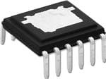
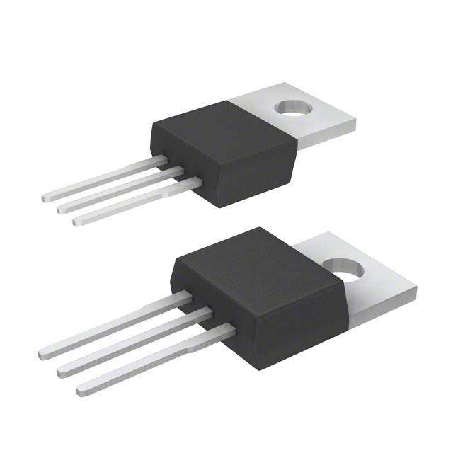
| 供应商器件封装 | eDIP-12 |
| 其它名称 | 596-1269-5 |
| 功率(W) | 22.5W |
| 包装 | 管件 |
| 商标 | Power Integrations |
| 安装风格 | Through Hole |
| 封装 | Tube |
| 封装/外壳 | 12-SDIP(0.412",10.46mm)裸焊盘 |
| 封装/箱体 | DIP-12 |
| 工作温度 | -40°C ~ 150°C |
| 工作温度范围 | - 40 C to + 150 C |
| 工厂包装数量 | 48 |
| 开关频率 | 132 kHz, 66 kHz |
| 标准包装 | 48 |
| 特色产品 | http://www.digikey.com/cn/zh/ph/PI/TopSwitchJX.html |
| 电压-击穿 | 725V |
| 电压-输入 | - |
| 电压-输出 | - |
| 电源电流 | 2.9 mA, 3.1 mA |
| 类型 | Off Line Switcher |
| 输出功率 | 12 W, 22.5 W |
| 输出电压 | 12 V |
| 输出隔离 | 隔离 |
| 配用 | /product-detail/zh/RDK-242/596-1312-ND/2403329 |
| 频率范围 | 66kHz ~ 132kHz |


- 商务部:美国ITC正式对集成电路等产品启动337调查
- 曝三星4nm工艺存在良率问题 高通将骁龙8 Gen1或转产台积电
- 太阳诱电将投资9.5亿元在常州建新厂生产MLCC 预计2023年完工
- 英特尔发布欧洲新工厂建设计划 深化IDM 2.0 战略
- 台积电先进制程称霸业界 有大客户加持明年业绩稳了
- 达到5530亿美元!SIA预计今年全球半导体销售额将创下新高
- 英特尔拟将自动驾驶子公司Mobileye上市 估值或超500亿美元
- 三星加码芯片和SET,合并消费电子和移动部门,撤换高东真等 CEO
- 三星电子宣布重大人事变动 还合并消费电子和移动部门
- 海关总署:前11个月进口集成电路产品价值2.52万亿元 增长14.8%


PDF Datasheet 数据手册内容提取
TOP264-271 TOPSwitch™-JX Family Integrated Off-Line Switcher with EcoSmart™ Technology for Highly Efficient Power Supplies Product Highlights + EcoSmart – Energy Efficient • Ideal for applications from 10 W to 245 W - • Energy efficient over entire load range • No-load consumption below 100 mW at 265 VAC • Up to 750 mW standby output power for 1 W input at 230 VAC High Design Flexibility for Low System Cost • Multi-mode PWM control maximizes efficiency at all loads • 132 kHz operation reduces transformer and power supply size • 66 kHz option for highest efficiency requirements • Accurate programmable current limit • Optimized line feed-forward for line ripple rejection • Frequency jittering reduces EMI filter cost • Fully integrated soft-start for minimum start-up stress Figure 1. Typical Flyback Application. • 725 V rated MOSFET • Simplifies meeting design derating requirements Extensive Protection Features • Auto-restart limits power delivery to <3% during overload faults • Output short-circuit protection (SCP) • Output over-current protection (OCP) • Output overload protection (OPP) • Output overvoltage protection (OVP) • User programmable for hysteretic/latching shutdown • Simple fast AC reset • Primary or secondary sensed eSIP-7C (E Package) eSOP-12B (K Package) eDIP-12B (V Package) • Line undervoltage (UV) detection prevents turn-off glitches Figure 2. Package Options. • Line overvoltage (OV) shutdown extends line surge withstand • Accurate thermal shutdown with large hysteresis (OTP) Description Advanced Package Options • eDIP™-12 package: TOPSwitch-JX cost effectively incorporates a 725 V power • 43 W / 117 W universal input power output capability with MOSFET, high-voltage switched current source, multi-mode PCB / metal heat sink PWM control, oscillator, thermal shutdown circuit, fault • Low profile horizontal orientation for ultra-slim designs protection and other control circuitry onto a monolithic device. • Heat transfer to both PCB and heat sink • Optional external heat sink provides thermal impedance Typical Applications equivalent to a TO-220 • Notebook or laptop adapter • eSIP™-7C package: • Generic adapter • 177 W universal input output power capability • Printer • Vertical orientation for minimum PCB footprint • LCD monitor • Simple heat sink mounting using clip provides thermal • Set-top box impedance equivalent to a TO-220 • PC or LCD TV standby • eSOP™-12 package: • Audio amplifier • 66 W universal input output power capability Output Power Ratings • Low profile surface mounted for ultra-slim designs See next page. • Heat transfer to PCB via exposed pad and SOURCE pins • Supports wave or reflow soldering • Extended creepage to DRAIN pin • Heat sink is connected to SOURCE for low EMI www.powerint.com August 2012 This Product is Covered by Patents and/or Pending Patent Applications.
TOP264-271 Output Power Table PCB Copper Area1 Metal Heat Sink1 230 VAC ±15%4 85-265 VAC 230 VAC ±15% 4 85-265 VAC Product5 Open Open Product5 Open Open Adapter2 Adapter2 Adapter2 Adapter2 Frame3 Frame3 Frame3 Frame3 TOP264VG 21 W 34 W 12 W 22.5 W TOP264EG/VG 30 W 62 W 20 W 43 W TOP264KG 30 W 49 W 16 W 30 W TOP265VG 22.5 W 36 W 15 W 25 W TOP265EG/VG 40 W 81 W 26 W 57 W TOP265KG 33 W 53 W 20 W 34 W TOP266VG 24 W 39 W 17 W 28.5 W TOP266EG/VG 60 W 119 W 40 W 86 W TOP266KG 36 W 58 W 23 W 39 W TOP267VG 27.5 W 44 W 19 W 32 W TOP267EG/VG 85 W 137 W 55 W 103 W TOP267KG 40 W 65 W 26 W 45 W TOP268VG 30 W 48 W 21.5 W 36 W TOP268EG/VG 105 W 148 W 70 W 112 W TOP268KG 46 W 73 W 30 W 50 W TOP269VG 32 W 51 W 22.5 W 37.5 W TOP269EG/VG 128 W 162 W 80 W 120 W TOP269KG 50 W 81 W 33 W 55 W TOP270VG 34 W 55 W 24.5 W 41 W TOP270EG/VG 147 W 190 W 93 W 140 W TOP270KG 56 W 91 W 36 W 60 W TOP271VG 36 W 59 W 26 W 43 W TOP271EG/VG 177 W 244 W 118 W 177 W TOP271KG 63 W 102 W 40 W 66 W Table 1. Output Power Table. Notes: 1. See Key Application Considerations section for more details. 2. Maximum continuous power in a typical non-ventilated enclosed adapter measured at +50 °C ambient temperature. 3. Maximum continuous power in an open frame design at +50 °C ambient temperature. 4. 230 VAC or 110/115 VAC with doubler. 5. Packages: E: eSIP-7C, V: eDIP-12, K: eSOP-12. See Part Ordering Information section. 2 Rev. E 08/12 www.powerint.com
TOP264-271 0 DRAIN (D) CONTROL (C) VC INTERNAL ZC 1 SUPPLY - SEHRURNOTR R AEMG-UPLLIAFTIEORR/ 54..88 VV +- SOFT START + + 5.8 V INTERNAL UV KPS(UPPER) - COMPARATOR IFB CURRENT VI (LIMIT) + LIMIT AD JUST ON/OFF ÷ 16 KPS(LOWER) - + SHUTDOWN/ EXTERNAL CURRENT AUTO-RESTART CURRENT LIMIT LIMIT (X) VBG + VT COMPARATOR MVOONLITTOARG E(V) 1 V STOP LOGIC HYTHSTEERRMEATLI C SOURCE (S) SHUTDOWN CONTROLLED V OVPOV/ TURN-ON SLEINNSEE DCMUAVX DCMAX SOTSOCPIL LSSATOTAOFRTRT DMAX GATE DRIVER FREQUENCY (F) 66k/132k WITH JITTER CLOCK S Q F REDUCTION R LEADING EDGE BLANKING F REDUCTION SOFT START KKPPSS((ULOPPWEERR)) IIIFPPBSS ((ULOPPWEERR)) PWM OFF PI-4511-012810 SOURCE (S) Figure 3. Functional Block Diagram. Pin Functional Description NO CONNECTION (NC) Pin: Internally not connected, floating potential pin. DRAIN (D) Pin: High-voltage power MOSFET DRAIN pin. The internal start-up bias current is drawn from this pin through a switched high- E Package voltage current source. Internal current limit sense point for (eSIP-7C) drain current. Exposed Pad Exposed Pad Internally (Hidden) CONTROL (C) Pin: Internally Connected to SOURCE Pin Error amplifier and feedback current input pin for duty cycle Connected to V Package control. Internal shunt regulator connection to provide internal SOURCE Pin (eDIP-12B) bias current during normal operation. It is also used as the S 12 1 V connection point for the supply bypass and auto-restart/ S 11 2 X compensation capacitor. 12345 7 S 10 3 C VXCFS D S 9 4 F EXTERNAL CURRENT LIMIT (X) Pin: Input pin for external current limit adjustment remote-ON/OFF S 8 and device reset. A connection to SOURCE pin disables all S 7 6 D functions on this pin. This pin should not be left floating. Exposed Pad (On Bottom) K Package VOLTAGE MONITOR (V) Pin: Internally Connected to SOURCE Pin (eSOP-12B) Input for OV, UV, line feed-forward with DC reduction, output MAX V 1 12 S overvoltage protection (OVP), remote-ON/OFF. A connection to X 2 11 S the SOURCE pin disables all functions on this pin. This pin should not be left floating. C 3 10 S F 4 9 S FREQUENCY (F) Pin: 8 S Input pin for selecting switching frequency 132 kHz if connected D 6 7 S to SOURCE pin and 66 kHz if connected to CONTROL pin. This pin should not be left floating. PI-5568-061011 SOURCE (S) Pin: Figure 4. Pin Configuration (Top View). Output MOSFET source connection for high-voltage power return. Primary-side control circuit common and reference point. 3 www.powerint.com Rev. E 08/12
TOP264-271 0 1 2 1 + RLS 4 MΩ VV FUO o VV r =V=R LIIUOSV V == ×× 4 1 RR 0MLL2SSΩ . ++8 VVVVVD ((ICIVV == IIUOVV)) PI-5579-11 %) 78 Auto-Restart Slope = PWM Gain VUOVV = 451 VDC cle ( VIonDlptCaugte D CONTVROL DDCCMMAAXX@@130705 VVDDCC == 7461%% Duty Cy C For R = 12 kΩ IL I = 61% S X LIMIT R See Figure 37 for CONTROL - 12IL kΩ other resistor values Current (R ) to select different IL I values. LIMIT %) 100 Figure 5. Package Line-Sense and Externally Set Current Limit. nt o ( urreRati TOP264-271 Functional Description k Cmit 55 Like TOPSwitch-HX, TOP264-271 is an integrated switched n Peaent Li mode power supply chip that converts a current at the control DraiCurr input to a duty cycle at the open drain output of a high-voltage To 25 power MOSFET. During normal operation the duty cycle of the power MOSFET decreases linearly with increasing CONTROL CCOuNrTreRnOt L pin current as shown in Figure 6. Full Frequency Mode In addition to the three terminal TOPSwitch features, such as 132 Low tlohoep h cigohm-vpoeltnasgaet isotna rcti-rucpu,i ttrhy,e acuytcol-er-ebsyt-acryt calned c uthrerermnta lilm shitiuntg-, kHz) FVreaqriuaebnlec y FreMqoudeen cy down, the TOP264-271 incorporates many additional functions y ( 66 Mode c that reduce system cost, increase power supply performance n and design flexibility. A patented high-voltage CMOS technology eque Jitter MMuoldtiu-Clayticolne allows both the high-voltage power MOSFET and all the low Fr voltage control circuitry to be cost effectively integrated onto a 30 single monolithic chip. I I I I I I CONTROL CD1 B C01 C02 C03 COFF Current Three terminals, FREQUENCY, VOLTAGE-MONITOR, and PI-5665-110609 EXTERNAL CURRENT LIMIT have been used to implement some of the new functions. These terminals can be connected Figure 6. Control Pin Characteristics (Multi-Mode Operation). to the SOURCE pin to operate the TOP264-271 in a TOPSwitch- like three terminal mode. However, even in this three terminal 6. Hysteretic over-temperature shutdown ensures thermal fault mode, the TOP264-271 offers many transparent features that do protection. not require any external components: 7. Packages with omitted pins and lead forming provide large drain creepage distance. 1. A fully integrated 17 ms soft-start significantly reduces or 8. Reduction of the auto-restart duty cycle and frequency to eliminates output overshoot in most applications by sweeping improve the protection of the power supply and load during both current limit and frequency from low to high to limit the open-loop fault, short-circuit, or loss of regulation. peak currents and voltages during start-up. 9. Tighter tolerances on I2f power coefficient, current limit 2. A maximum duty cycle (DC ) of 78% allows smaller input reduction, PWM gain and thermal shutdown threshold. MAX storage capacitor, lower input voltage requirement and/or higher power capability. The VOLTAGE-MONITOR (V) pin is usually used for line sensing 3. Multi-mode operation optimizes and improves the power by connecting a 4 MW resistor from this pin to the rectified DC supply efficiency over the entire load range while maintaining high-voltage bus to implement line overvoltage (OV), under- good cross regulation in multi-output supplies. voltage (UV) and dual-slope line feed-forward with DC MAX 4. Switching frequency of 132 kHz reduces the transformer size reduction. In this mode, the value of the resistor determines the with no noticeable impact on EMI. OV/UV thresholds and the DC is reduced linearly with a dual MAX 5. Frequency jittering reduces EMI in the full frequency mode at slope to improve line ripple rejection. In addition, it also high-load condition. provides another threshold to implement the latched and 4 Rev. E 08/12 www.powerint.com
TOP264-271 hysteretic output overvoltage protection (OVP). The pin can MOSFET off and puts the control circuitry in a low current also be used as a remote-ON/OFF using the I threshold. standby mode. The high-voltage current source turns on and UV charges the external capacitance again. A hysteretic internal The EXTERNAL CURRENT LIMIT (X) pin can be used to reduce supply undervoltage comparator keeps V within a window of C the current limit externally to a value close to the operating peak typically 4.8 V to 5.8 V by turning the high-voltage current current, by connecting the pin to SOURCE through a resistor. source on and off as shown in Figure 8. The auto-restart circuit This pin can also be used as a remote-ON/OFF input. has a divide-by-sixteen counter, which prevents the output MOSFET from turning on again until sixteen discharge/charge The FREQUENCY (F) pin sets the switching frequency in the full cycles have elapsed. This is accomplished by enabling the frequency PWM mode to the default value of 132 kHz when output MOSFET only when the divide-by-sixteen counter connected to SOURCE pin. A half frequency option of 66 kHz reaches the full count (S15). The counter effectively limits can be chosen by connecting this pin to the CONTROL pin TOP264-271 power dissipation by reducing the auto-restart instead. Leaving this pin open is not recommended. duty cycle to typically 2%. Auto-restart mode continues until output voltage regulation is again achieved through closure of CONTROL (C) Pin Operation the feedback loop. The CONTROL pin is a low impedance node that is capable of receiving a combined supply and feedback current. During Oscillator and Switching Frequency normal operation, a shunt regulator is used to separate the The internal oscillator linearly charges and discharges an feedback signal from the supply current. CONTROL pin voltage internal capacitance between two voltage levels to create a V is the supply voltage for the control circuitry including the triangular waveform for the timing of the pulse width modulator. C MOSFET gate driver. An external bypass capacitor closely This oscillator sets the pulse width modulator/current limit latch connected between the CONTROL and SOURCE pins is at the beginning of each cycle. required to supply the instantaneous gate drive current. The total amount of capacitance connected to this pin also sets the The nominal full switching frequency of 132 kHz was chosen to auto-restart timing as well as control loop compensation. minimize transformer size while keeping the fundamental EMI When rectified DC high-voltage is applied to the DRAIN pin frequency below 150 kHz. The FREQUENCY pin, when shorted during start-up, the MOSFET is initially off, and the CONTROL to the CONTROL pin, lowers the full switching frequency to pin capacitor is charged through a switched high-voltage 66 kHz (half frequency), which may be preferable in some cases current source connected internally between the DRAIN and such as noise sensitive video applications or a high efficiency CONTROL pins. When the CONTROL pin voltage V reaches standby mode. Otherwise, the FREQUENCY pin should be C approximately 5.8 V, the control circuitry is activated and the connected to the SOURCE pin for the default 132 kHz. soft-start begins. The soft-start circuit gradually increases the drain peak current and switching frequency from a low starting To further reduce the EMI level, the switching frequency in the value to the maximum drain peak current at the full frequency full frequency PWM mode is jittered (frequency modulated) by over approximately 17 ms. If no external feedback/supply approximately ±2.5 kHz for 66 kHz operation or ±5 kHz for current is fed into the CONTROL pin by the end of the soft-start, 132 kHz operation at a 250 Hz (typical) rate as shown in Figure 7. the high-voltage current source is turned off and the CONTROL The jitter is turned off gradually as the system is entering the pin will start discharging in response to the supply current variable frequency mode with a fixed peak drain current. drawn by the control circuitry. If the power supply is designed properly, and no fault condition such as open-loop or shorted Pulse Width Modulator output exists, the feedback loop will close, providing external The pulse width modulator implements multi-mode control by CONTROL pin current, before the CONTROL pin voltage has driving the output MOSFET with a duty cycle inversely had a chance to discharge to the lower threshold voltage of proportional to the current into the CONTROL pin that is in approximately 4.8 V (internal supply undervoltage lockout excess of the internal supply current of the chip (see Figure 6). threshold). When the externally fed current charges the CONTROL The feedback error signal, in the form of the excess current, is pin to the shunt regulator voltage of 5.8 V, current in excess of filtered by an RC network with a typical corner frequency of the consumption of the chip is shunted to SOURCE through an 7 kHz to reduce the effect of switching noise in the chip supply NMOS current mirror as shown in Figure 3. The output current current generated by the MOSFET gate driver. of that NMOS current mirror controls the duty cycle of the power MOSFET to provide closed loop regulation. The shunt To optimize power supply efficiency, four different control regulator has a finite low output impedance Z that sets the gain modes are implemented. At maximum load, the modulator C of the error amplifier when used in a primary feedback operates in full frequency PWM mode; as load decreases, the configuration. The dynamic impedance Z of the CONTROL pin modulator automatically transitions, first to variable frequency C together with the external CONTROL pin capacitance sets the PWM mode, then to low frequency PWM mode. At light load, dominant pole for the control loop. the control operation switches from PWM control to multi-cycle- modulation control, and the modulator operates in multi-cycle- When a fault condition such as an open-loop or shorted output modulation mode. Although different modes operate differently prevents the flow of an external current into the CONTROL pin, to make transitions between modes smooth, the simple the capacitor on the CONTROL pin discharges towards 4.8 V. relationship between duty cycle and excess CONTROL pin At 4.8 V, auto-restart is activated, which turns the output current shown in Figure 6 is maintained through all three PWM 5 www.powerint.com Rev. E 08/12
TOP264-271 FSrweqitucehnincgy fOSC + PI-4530-041107 MTvMahOaleuxN emi ImToaOfux 7Rmim8 %tuDom ut(ht tydeypu rCitceyyca cctl)i.fiyl eec Hdleo ,D wDCeC vhMeigAr,Xh ,b -ivyso csltoeatng anete bacu tdisne gtfh atrhuoelut gmVhOa aLx TirmeAsGuimsEto- r f - OSC with appropriate value (4 MW typical), the maximum duty cycle can be made to decrease from 78% to 40% (typical) when input 4 ms line voltage increases from 88 V to 380 V, with dual gain slopes. Error Amplifier VDRAIN The shunt regulator can also perform the function of an error amplifier in primary-side feedback applications. The shunt Time regulator voltage is accurately derived from a temperature- compensated bandgap reference. The CONTROL pin dynamic impedance Z sets the gain of the error amplifier. The CONTROL Figure 7. Switching Frequency Jitter (Idealized VDRAIN Waveforms). pin clamps exCternal circuit signals to the V voltage level. The C modes. Please see the following sections for the details of the CONTROL pin current in excess of the supply current is operation of each mode and the transitions between modes. separated by the shunt regulator and becomes the feedback current I for the pulse width modulator. FB Full Frequency PWM mode: The PWM modulator enters full frequency PWM mode when the CONTROL pin current (I ) On-Chip Current Limit with External Programmability C reaches I . In this mode, the average switching frequency is The cycle-by-cycle peak drain current limit circuit uses the B kept constant at f (pin selectable 132 kHz or 66 kHz). Duty output MOSFET ON-resistance as a sense resistor. A current OSC cycle is reduced from DC through the reduction of the on-time limit comparator compares the output MOSFET ON-state drain MAX when I is increased beyond I . This operation is identical to the to source voltage V with a threshold voltage. High drain C B DS(ON) PWM control of all other TOPSwitch families. TOP264-271 only current causes V to exceed the threshold voltage and turns DS(ON) operates in this mode if the cycle-by-cycle peak drain current the output MOSFET off until the start of the next clock cycle. stays above k × I (set), where k is 55% (typical) The current limit comparator threshold voltage is temperature PS(UPPER) LIMIT PS(UPPER) and I (set) is the current limit externally set via the EXTERNAL compensated to minimize the variation of the current limit due LIMIT CURRENT LIMIT (X) pin. to temperature related changes in R of the output MOSFET. DS(ON) The default current limit of TOP264-271 is preset internally. Variable Frequency PWM mode: When peak drain current is However, with a resistor connected between EXTERNAL lowered to k × I (set) as a result of power supply load CURRENT LIMIT (X) pin and SOURCE pin, current limit can be PS(UPPER) LIMIT reduction, the PWM modulator initiates the transition to variable programmed externally to a lower level between 30% and 100% frequency PWM mode, and gradually turns off frequency jitter. of the default current limit. By setting current limit low, a larger In this mode, peak drain current is held constant at k × TOP264-271 than necessary for the power required can be used PS(UPPER) I (set) while switching frequency drops from the initial full to take advantage of the lower R for higher efficiency/ LIMIT DS(ON) frequency of f (132 kHz or 66 kHz) towards the minimum smaller heat sinking requirements. With a second resistor OSC frequency of f (30 kHz typical). Duty cycle reduction is connected between the EXTERNAL CURRENT LIMIT (X) pin MCM(MIN) accomplished by extending the off-time. and the rectified DC high-voltage bus, the current limit is reduced with increasing line voltage, allowing a true power Low Frequency PWM mode: When switching frequency limiting operation against line variation to be implemented. When reaches f (30 kHz typical), the PWM modulator starts to using an RCD clamp, this power limiting technique reduces MCM(MIN) transition to low frequency mode. In this mode, switching maximum clamp voltage at high-line. This allows for higher frequency is held constant at f and duty cycle is reduced, reflected voltage designs as well as reducing clamp dissipation. MCM(MIN) similar to the full frequency PWM mode, through the reduction of the on-time. Peak drain current decreases from the initial The leading edge blanking circuit inhibits the current limit value of k × I (set) towards the minimum value of comparator for a short time after the output MOSFET is turned PS(UPPER) LIMIT k × I (set), where k is 25% (typical) and I (set) on. The leading edge blanking time has been set so that, if a PS(LOWER) LIMIT PS(LOWER) LIMIT is the current limit externally set via the X pin. power supply is designed properly, current spikes caused by primary-side capacitances and secondary-side rectifier reverse Multi-Cycle-Modulation mode: When peak drain current is recovery time should not cause premature termination of the lowered to k × I (set), the modulator transitions to switching pulse. The current limit is lower for a short period PS(LOWER) LIMIT multi-cycle-modulation mode. In this mode, at each turn-on, after the leading edge blanking time. This is due to dynamic the modulator enables output switching for a period of T characteristics of the MOSFET. During start-up and fault MCM(MIN) at the switching frequency of f (4 or 5 consecutive pulses conditions the controller prevents excessive drain currents by MCM(MIN) at 30 kHz) with the peak drain current of k × I (set), reducing the switching frequency. PS(LOWER) LIMIT and stays off until the CONTROL pin current falls below I . C(OFF) This mode of operation not only keeps peak drain current low Line Undervoltage Detection (UV) but also minimizes harmonic frequencies between 6 kHz and At power-up, UV keeps TOP264-271 off until the input line 30 kHz. By avoiding transformer resonant frequency this way, voltage reaches the undervoltage threshold. At power-down, all potential transformer audible noises are greatly suppressed. 6 Rev. E 08/12 www.powerint.com
TOP264-271 ~~ ~~ V UV V ~~ ~~ ~~ LINE 0 V S15 S14 S13 S~1~2 S0 S15 S14 S13 S~1~2 S0 S15 S14 S13 S~1~2 S0 S15 S15 5.8 V V 4.8 V C 0 V ~~ ~~ V DRAIN ~~ 0 V V OUT 0 V ~~ ~~ ~~ 1 2 3 2 4 Note: S0 through S15 are the output states of the auto-restart counter PI-4531-121206 Figure 8. Typical Waveforms for (1) Power-Up (2) Normal Operation (3) Auto-Restart (4) Power-Down. UV prevents auto-restart attempts after the output goes out of In order to reduce the no-load input power of TOP264-271 regulation. This eliminates power-down glitches caused by designs, the V pin operates at very low currents. This requires slow discharge of the large input storage capacitor present in careful layout considerations when designing the PCB to avoid applications such as standby supplies. A single resistor noise coupling. Traces and components connected to the V pin connected from the VOLTAGE-MONITOR pin to the rectified DC should not be adjacent to any traces carrying switching currents. high-voltage bus sets UV threshold during power-up. Once the These include the drain, clamp network, bias winding return or power supply is successfully turned on, the UV threshold is power traces from other converters. If the line sensing features lowered to 44% of the initial UV threshold to allow extended are used, then the sense resistors must be placed within 10 mm input voltage operating range (UV low threshold). If the UV low of the V pin to minimize the V pin node area. The DC bus threshold is reached during operation without the power supply should then be routed to the line-sense resistors. Note that losing regulation, the device will turn off and stay off until UV external capacitance must not be connected to the V pin as this (high threshold) has been reached again. If the power supply may cause misoperation of the V pin related functions. loses regulation before reaching the UV low threshold, the device will enter auto-restart. At the end of each auto-restart Hysteretic or Latching Output Overvoltage Protection (OVP) cycle (S15), the UV comparator is enabled. If the UV high The detection of the hysteretic or latching output overvoltage threshold is not exceeded, the MOSFET will be disabled during protection (OVP) is through the trigger of the line overvoltage the next cycle (see Figure 8). The UV feature can be disabled threshold. The V pin voltage will drop by 0.5 V, and the independent of the OV feature. controller measures the external attached impedance immediately after this voltage drops. If I exceeds I (336 mA typical) V OV(LS) Line Overvoltage Shutdown (OV) longer than 100 ms, TOP264-271 will latch into a permanent The same resistor used for UV also sets an overvoltage off-state for the latching OVP. It only can be reset if I exceeds X threshold, which, once exceeded, will force TOP264-271 to I = -27 mA (typ) or V goes below the power-up reset X(TH) C stop switching instantaneously (after completion of the current threshold (V ) and then back to normal. If I does not C(RESET) V switching cycle). If this condition lasts for at least 100 ms, the exceed I or exceeds no longer than 100 ms, TOP264-271 OV(LS) TOP264-271 output will be forced into off state. When the line will initiate the line overvoltage and the hysteretic OVP. Their voltage is back to normal with a small amount of hysteresis behavior will be identical to the line overvoltage shutdown (OV) provided on the OV threshold to prevent noise triggering, the that has been described in detail in the previous section. state machine sets to S13 and forces TOP264-271 to go During a fault condition resulting from loss of feedback, output through the entire auto-restart sequence before attempting to voltage will rapidly rise above the nominal voltage. The increase switch again. The ratio of OV and UV thresholds is preset at in output voltage will also result in an increase in the voltage at 4.5, as can be seen in Figure 9. When the MOSFET is off, the the output of the bias winding. A voltage at the output of the rectified DC high-voltage surge capability is increased to the bias winding that exceeds of the sum of the voltage rating of the voltage rating of the MOSFET (725 V), due to the absence of the Zener diode connected from the bias winding output to the V reflected voltage and leakage spikes on the drain. The OV pin and V pin voltage, will cause a current in excess of I to be V feature can be disabled independent of the UV feature. injected into the V pin, which will trigger the OVP feature. 7 www.powerint.com Rev. E 08/12
TOP264-271 If the power supply is operating under heavy load or low input Remote-ON/OFF line conditions when an open-loop occurs, the output voltage TOP264-271 can be turned on or off by controlling the current into may not rise significantly. Under these conditions, a latching the VOLTAGE-MONITOR pin or out from the EXTERNAL CURRENT shutdown will not occur until load or line conditions change. LIMIT pin. In addition, the VOLTAGE-MONITOR pin has a 1 V Nevertheless, the operation provides the desired protection by threshold comparator connected at its input. This voltage preventing significant rise in the output voltage when the line or threshold can also be used to perform remote-ON/OFF control. load conditions do change. Primary-side OVP protection with the TOP264-271 in a typical application will prevent a nominal When a signal is received at the VOLTAGE-MONITOR pin or the 12 V output from rising above approximately 20 V under open- EXTERNAL CURRENT LIMIT pin to disable the output through loop conditions. If greater accuracy is required, a secondary any of the pin functions such as OV, UV and remote-ON/OFF, sensed OVP circuit is recommended. TOP264-271 always completes its current switching cycle before the output is forced off. Line Feed-Forward with DC Reduction MAX The same resistor used for UV and OV also implements line voltage As seen above, the remote-ON/OFF feature can also be used feed-forward, which minimizes output line ripple and reduces as a standby or power switch to turn off the TOP264-271 and power supply output sensitivity to line transients. Note that for the keep it in a very low power consumption state for indefinitely long same CONTROL pin current, higher line voltage results in smaller periods. If the TOP264-271 is held in remote-off state for long operating duty cycle. As an added feature, the maximum duty enough time to allow the CONTROL pin to discharge to the cycle DC is also reduced from 78% (typical) at a voltage slightly internal supply undervoltage threshold of 4.8 V (approximately MAX lower than the UV threshold to 36% (typical) at the OV threshold. 32 ms for a 47 mF CONTROL pin capacitance), the CONTROL DC of 36% at high-line was chosen to ensure that the power pin goes into the hysteretic mode of regulation. In this mode, MAX capability of the TOP264-271 is not restricted by this feature under the CONTROL pin goes through alternate charge and discharge normal operation. TOP264-271 provides a better fit to the ideal cycles between 4.8 V and 5.8 V (see CONTROL pin operation feed-forward by using two reduction slopes: -1% per mA for all bus section above) and runs entirely off the high-voltage DC input, voltage less than 195 V (typical for 4 MW line impedance) and but with very low power consumption (<100 mW typical at -0.25% per mA for all bus voltage more than 195 V. 230 VAC with X pin open). When the TOP264-271 is remotely Voltage Monitor and External Current Limit Pin Table* Figure Number 13 14 15 16 17 18 19 20 21 22 23 24 Three Terminal Operation 3 Line Undervoltage (UV) 3 3 3 3 3 Line Overvoltage (OV) 3 3 3 3 3 Line Feed-Forward (DC ) 3 3 3 3 MAX Output Overvoltage Protection (OVP) 3 Overload Power Limiting (OPP) 3 External Current Limit 3 3 3 3 3 3 Remote-ON/OFF 3 3 3 Device Reset 3 3 3 Fast AC Reset 3 AC Brown-Out 3 *This table is only a partial list of many VOLTAGE MONITOR and EXTERNAL CURRENT LIMIT Pin Configurations that are possible. Table 2. VOLTAGE MONITOR (V) Pin and EXTERNAL CURRENT LIMIT (X) Pin Configuration Options. 8 Rev. E 08/12 www.powerint.com
TOP264-271 X Pin V Pin I I I I REM(N) UV OV OV(LS) (Enabled) Output (Non-Latching) (Latching) MOSFET Switching (Disabled) Disabled when supply I output goes out of regulation I (Default) LIMIT Current Limit I DC (78%) MAX Maximum Duty Cycle I V BG Pin Voltage I -250 -200 -150 -100 -50 0 25 50 75 100 125 336 X and V Pins Current (µA) Note: This figure provides idealized functional characteristics with typical performance values. Please refer to the parametric table and typical performance characteristics sections of the data sheet for measured data. For a detailed description of each functional pin operation refer to the Functional Description section of the data sheet. PI-5528-060409 Figure 9. VOLTAGE MONITOR and EXTERNAL CURRENT LIMIT Pin Characteristics. turned on after entering this mode, it will initiate a normal Soft-Start start-up sequence with soft-start the next time the CONTROL The 17 ms soft-start sweeps the peak drain current and switching pin reaches 5.8 V. In the worst-case, the delay from remote-on frequency linearly from minimum to maximum value by operating to start-up can be equal to the full discharge/charge cycle time through the low frequency PWM mode and the variable of the CONTROL pin, which is approximately 125 ms for a frequency mode before entering the full frequency mode. In 47 mF CONTROL pin capacitor. This reduced consumption addition to start-up, soft-start is also activated at each restart remote-off mode can eliminate expensive and unreliable in-line attempt during auto-restart and when restarting after being in mechanical switches. It also allows for microprocessor hysteretic regulation of CONTROL pin voltage (V ), due to C controlled turn-on and turn-off sequences that may be required remote-off or thermal shutdown conditions. This effectively in certain applications such as inkjet and laser printers. minimizes current and voltage stresses on the output MOSFET, 9 www.powerint.com Rev. E 08/12
TOP264-271 the clamp circuit and the output rectifier during start-up. This mode, and a 4.8 V to 5.8 V (typical) triangular waveform is feature also helps minimize output overshoot and prevents present on the CONTROL pin while in thermal shutdown. saturation of the transformer during start-up. Bandgap Reference Shutdown/Auto-Restart (for OCP, SCP, OPP) All critical TOP264-271 internal voltages are derived from a To minimize TOP264-271 power dissipation under fault temperature-compensated bandgap reference. This voltage conditions such as over current (OC), short-circuit (SC) or over reference is used to generate all other internal current references, power (OP), the shutdown/auto-restart circuit turns the power which are trimmed to accurately set the switching frequency, supply on and off at an auto-restart duty cycle of typically 2% if MOSFET gate drive current, current limit, and the line OV/UV/ an out of regulation condition persists. Loss of regulation OVP thresholds. TOP264-271 has improved circuitry to interrupts the external current into the CONTROL pin. V maintain all of the above critical parameters within very tight C regulation changes from shunt mode to the hysteretic auto- absolute and temperature tolerances. restart mode as described in CONTROL pin operation section. When the fault condition is removed, the power supply output High-Voltage Bias Current Source becomes regulated, V regulation returns to shunt mode, and This high-voltage current source biases TOP264-271 from the C normal operation of the power supply resumes. DRAIN pin and charges the CONTROL pin external capacitance during start-up or hysteretic operation. Hysteretic operation Hysteretic Over-Temperature Protection (OTP) occurs during auto-restart, remote-off and over-temperature Temperature protection is provided by a precision analog circuit shutdown. In this mode of operation, the current source is that turns the output MOSFET off when the junction temperature switched on and off, with an effective duty cycle of approxi- exceeds the thermal shutdown temperature (142 °C typical). mately 35%. This duty cycle is determined by the ratio of When the junction temperature cools to below the lower CONTROL pin charge (I ) and discharge currents (I and I ). C CD1 CD2 hysteretic temperature point, normal operation resumes, thus This current source is turned off during normal operation when providing automatic recovery. A large hysteresis of 75 °C the output MOSFET is switching. The effect of the current (typical) is provided to prevent overheating of the PC board due source switching will be seen on the DRAIN voltage waveform to a continuous fault condition. V is regulated in hysteretic as small disturbances and is normal. C 10 Rev. E 08/12 www.powerint.com
TOP264-271 CONTROL (C) 200 µA (Negative Current Sense - ON/OFF, Current Limit Adjustment, OVP Latch Reset) V + V BG T EXTERNAL CURRENT LIMIT (X) VOLTAGE MONITOR (V) (Voltage Sense, ON/OFF) 1 V VREF (Positive Current Sense - Undervoltage, Overvoltage, ON/OFF, Maximum Duty Cycle Reduction, Output Over- voltage Protection) 400 µA PI-5567-030910 Figure 10. VOLTAGE MONITOR (V) and EXTERNAL CURRENT LIMIT (X) Pin Input Simplified Schematic. 11 www.powerint.com Rev. E 08/12
TOP264-271 Typical Uses of FREQUENCY (F) Pin + + DC D DC D Input Input Voltage CONTROL Voltage CONTROL C C S F S F - - PI-2654-071700 PI-2655-071700 Figure 11. Full Frequency Operation (132 kHz). Figure 12. Half Frequency Operation (66 kHz). 12 Rev. E 08/12 www.powerint.com
TOP264-271 Typical Uses of VOLTAGE MONITOR (V) and EXTERNAL CURRENT LIMIT (X) Pins V Package (eDIP-12) + E Package S 12 1 V + VUV = IUV × RLS + VV (IV = IUV) (eSIP-7C) S 11 2 X VOV = IOV × RLS + VV (IV = IOV) S 10 3 C S 9 4 F For R = 4 MΩ LS S 8 R 4 MΩ VUV = 102.8 VDC VXCFS D S 7 6 D LS VOV = 451 VDC DC S DC Input D C Input DCMAX@100 VDC = 76% Voltage K Package (eSOP-12) Voltage DCMAX@375 VDC = 41% D V C S D 1 V S 12 D V CONTROL 2 X S 11 CONTROL C 3 C S 10 C 4 F S 9 S 8 - S X F 6 D S 7 - S S C D PI-6119-061011 PI-4717-120307 Figure 13. Three Terminal Operation (VOLTAGE MONITOR and EXTERNAL Figure 14. Line-Sensing for Undervoltage, Overvoltage and Line Feed-Forward. CURRENT LIMIT Features Disabled. FREQUENCY Pin Tied to SOURCE or CONTROL Pin.) V = I × R +V (I = I ) UV UV LS V V UV + VOV = IOV × RLS + VV (IV = IOV) + V = R × I +V (I = I ) UV LS UV V V UV For R = 4 MΩ LS 4 MΩ V = 102.8 VDC For Values Shown UV VOV = 451 VDC VUV = 103.8 VDC RLS 4 MΩ Sense Output Voltage RLS DC VR ROVP DC Input OVP DC @ 100 VDC = 76% Input 40 kΩ Voltage DCMAX @ 375 VDC = 41% Voltage MAX D V D V CONTROL CONTROL C C R >3kΩ 6.2 V OVP - S - S PI-4719-120307 PI-4720-120307 Figure 15. Line-Sensing for Undervoltage, Overvoltage, Line Feed-Forward and Figure 16. Line-Sensing for Undervoltage Only (Overvoltage Disabled). Hysteretic Output Overvoltage Protection. + + VOV = IOV × RLS + VV (IV = IOV) F o Ir RIL == 1621 %kΩ 4 MΩ LIMIT For Values Shown V = 457.2 VDC For RIL = 19 kΩ RLS OV ILIMIT = 37% DC DC See Figure 37 for other Input 55 kΩ Input D resistor values (RIL). Voltage Voltage CONTROL D V 1N4148 C CONTROL C S X R - S - IL PI-4721-120307 PI-5580-111210 Figure 17. Line-Sensing for Overvoltage Only (Undervoltage Disabled). Maximum Figure 18. External Set Current Limit. Duty Cycle Reduced at Low-Line and Further Reduction with Increasing Line Voltage. 13 www.powerint.com Rev. E 08/12
TOP264-271 Typical Uses of VOLTAGE MONITOR (V) and EXTERNAL CURRENT LIMIT (X) Pins (cont.) + ILIMIT =100% @ 100 VDC + Q can be an optocoupler ILIMIT = 53% @ 300 VDC ouRtput or can be replaced by RLS 2.5 MΩ a manual switch. DC DC Input D Input D Voltage CONTROL Voltage CONTROL C C S X S X - R6 IkLΩ - QR 47 KΩ ON/OFF PI-5465-061009 PI-5466-061009 Figure 19. Current Limit Reduction with Line Voltage. Figure 20. Active-On (Fail Safe) Remote-ON/OFF, and Latch Reset. + + V = I × R +V (I = I ) Q can be an optocoupler UV UV LS V V UV ouRtput or can be replaced VOV = IOV × RLS + VV (IV = IoV) by a manual switch. DC @100 VDC = 76% R 4 MΩ MAX LS DC @375 VDC = 41% For RIL =12 kΩ MAX DC ILIMIT = 61% DC oQuRt pcuatn o br ec aann boep troecpolaucpeledr Input D For RIL =19 kΩ Input D V by a manual switch. Voltage CONTROL C ILIMIT = 37% Voltage CONTROL C For RIL =12 kΩ ILIMIT = 61% S X S X - RIL QR 16 kΩ ON/OFF - RIL QR 16 kΩ ON/OFF PI-5531-072309 PI-5467-061009 Figure 21. Active-On Remote-ON/OFF with Externally Set Current Limit, Figure 22. Active-On Remote-ON/OFF with Line-Sense and External and Latch Reset Current Limit, and Latch Reset. 0 1 2 1 + VVUOVV == IIUOVV xx RRLLSS ++ VVVV ((IIVV == IIUoVV)) 565-11 + T<3yp s. A65C VlaAtcCh b rreoswent otiumt eth.reshold. R 4 MΩ For RLS = 4 MΩ PI-5 dHeigchreear sginagin CQ1R faolrl olowwse irn cnroe-alosaindg i nRp1u/t LS VUV = 102.8 VDC power. VOV = 451 VDC D InDpCut D V DDCCMMAAXX @@ 130705 VVDDCC == 7461%% InDpCut CONTROL C Voltage CONTROL Voltage C For R = 12 kΩ S X R1 S X ILIMIILT = 61% RIL QR 4 MΩ 1N4007 See Figure 37 for AC RIL other resistor values R2 C1 Input - 12 kΩ (R ) to select different - 39 kΩ 47 nF IL I values. LIMIT PI-5652-110609 Figure 23. Line Sensing and Externally Set Current Limit. Figure 24. Externally Set Current Limit, Fast AC Latch Reset and Brown-Out. 14 Rev. E 08/12 www.powerint.com
TOP264-271 Application Example Low No-Load, High Efficiency, 65 W, Universal Input Line-Sense Resistor Values Adapter Power Supply • Increasing line-sensing resistance from 4 MW to 10.2 MW to reduce no-load input power dissipation by 16 mW The circuit shown in Figure 25 shows a 90 VAC to 265 VAC input, 19 V, 3.42 A output power supply, designed for operation Line-sensing is provided by resistors R3 and R4 and sets the inside a sealed adapter case type. The goals of the design were line undervoltage and overvoltage thresholds. The combined highest full load efficiency, highest average efficiency (average of value of these resistors was increased from the standard 4 MW 25%, 50%, 75% and 100% load points), and very low no-load to 10.2 MW. This reduced the resistor dissipation, and therefore consumption. Additional requirements included latching output contribution to no-load input power, from ~26 mW to ~10 mW. To overvoltage shutdown and compliance to safety agency limited compensate the resultant change in the UV (turn-on) threshold power source (LPS) limits. Measured efficiency and no-load resistor R20 was added between the CONTROL and VOLTAGE- performance is summarized in the table shown in the schematic MONITOR pins. This adds a DC current equal to ~16 mA into the which easily exceed current energy efficiency requirements. VOLTAGE MONITOR pin, requiring only 9 mA to be provided via R3 and R4 to reach the VOLTAGE MONITOR pin UV (turn-on) In order to meet these design goals the following key design threshold current of 25 mA and setting the UV threshold to 95 VDC. decisions were made. This technique does effectively disable the line OV feature as PI Part Selection the resultant OV threshold is raised from ~450 VDC to ~980 VDC. • One device size larger selected than required for power However in this design there was no impact as the value of delivery to increase efficiency input capacitance (C2) was sufficient to allow the design to withstand differential line surges greater than 2 kV without the The current limit programming feature of TOPSwitch-JX allows peak drain voltage reaching the BV rating of U1. DSS the selection of a larger device than needed for power delivery. This gives higher full load, low-line efficiency by reducing the Specific guidelines and detailed calculations for the value of MOSFET conduction losses (I 2 × R ) but maintains the R20 may be found in the TOPSwitch-JX Application Note (AN-47). RMS DS(ON) overload power, transformer and other components size as if a smaller device had been used. Clamp Configuration – RZCD vs RCD • An RZCD (Zener bleed) was selected over an RCD clamp to For this design one device size larger than required for power give higher light load efficiency and lower no-load consumption delivery (as recommended by the power table) was selected. This typically gives the highest efficiency. Further increases in The clamp network is formed by VR2, C4, R5, R6, R11, R28, device size often results in the same or lower efficiency due to R29 and D2. It limits the peak drain voltage spike caused by the larger switching losses associated with a larger MOSFET. leakage inductance to below the BV rating of the internal DSS Input Voltage (VAC) 90 115 230 C11 C12 Full Power Efficiency (%) 86.6 88.4 89.1 1 nF 1 nF R15 250 VAC 100 V 33 Ω Average Efficiency (%) 89.8 89.5 C13 C14 No-load Input Power (mW) 57.7 59.7 86.7 VR2 T1 470 µF 470 µF SMAJ250A 3 RM10FL1 25 V 25 V 19 V, 3.42 A G6B0DU01 8VJ 30R05 Ω 10603C004 pVF FL2 V30D1500C 15C002 n1VF R11 15R06 Ω 3R002 8Ω RTN 300 Ω 1 5 5.1R M3Ω 10R M7Ω 21.C2 k 5nVF 3R002 9Ω RDS12K 4BAV7D2-14FWS- 53C651 µ0VF 2R0 1k6Ω 1.R62 k2Ω C19 12L m3H R24 MMBQT14403 2R01 Ω4 47C01 5pF 65.80 nVF R4 R8 2.2 Ω 50 V 2.2R 2M1373Ω5C0 V1 2nA.F2CR M2Ω 1420C002 µVF 5.1 MΩ 10 MΩ BA1V9DR1113%29 k0WΩS222C509 VnF ZM4M.R7V51 R2k241Ω4B-71RP0011SU -02ΩH35B-0A1- P1SU-2H35A-0A1- 1R104 2R1k77Ω%1 k7Ω Q2 20L04 µH D V R25 MMBT3904 C16 TOPSwUi1tch-JX CONTROL C 12/08 ΩW 2520 nVF F1 TOP269EG 4 A R13 S X F 6.8 Ω R19 L C6 1/8 W 20 kΩ N 90V A- C265 111R %k9Ω 15000 VnF 417C6 7 µVF 150C002 2VnF LMV41U3%21AIMF 1R01 %1k8Ω PI-5667-030810 Figure 25. Schematic of High Efficiency 19 V, 65 W, Universal Input Flyback Supply with Low No-load. 15 www.powerint.com Rev. E 08/12
TOP264-271 TOPSwitch-JX MOSFET. This arrangement was selected over To minimize the dissipation from the bias winding under no-load a standard RCD clamp to improve light load efficiency and no-load conditions the number of bias winding turns and value of C10 input power. was adjusted to give a minimum voltage across C10 of ~9 V. This is the minimum required to keep the optocoupler biased. In a standard RCD clamp C4 would be discharged by a parallel To minimize the dissipation of the secondary-side feedback resistor rather than a resistor and series Zener. In an RCD clamp circuit Q2 was added to form a Darlington connection with U3B. the resistor value is selected to limit the peak drain voltage This reduced the feedback current on the secondary to ~1 mA. under full load and overload conditions. However under light or The increased loop gain (due to the h of the transistor) was FE no-load conditions this resistor value now causes the capacitor compensated by increasing the value of R16 and the addition of voltage to discharge significantly as both the leakage inductance R25. A standard 2.5 V TL431 voltage reference was replaced energy and switching frequency are lower. As the capacitor has with the 1.24 V LMV431 to reduce the supply current requirement to be recharged to above the reflected output voltage each from 1 mA to 100 mA. switching cycle the lower capacitor voltage represents wasted energy. It has the effect of making the clamp dissipation Output Rectifier Choice appear as a significant load just as if it were connected to the • Higher current rating, low V Schottky rectifier diode selected F output of the power supply. for output rectifier. The RZCD arrangement solves this problem by preventing the A dual 15 A, 100 V Schottky rectifier diode with a V of 0.455 V F voltage across the capacitor discharging below a minimum at 5 A was selected for D5. This is a higher current rating than value (defined by the voltage rating of VR2) and therefore required to reduce resistive and forward voltage losses to improve minimizing clamp dissipation under light and no-load conditions. both full load and average efficiency. The use of a 100 V Schottky was possible due to the high transformer primary to secondary Resistors R6 and R28 provide damping of high frequency turns ratio (V = 110 V) which was in turn possible due to the OR ringing to reduce EMI. Due to the resistance in series with VR2, high-voltage rating of the TOPSwitch-JX internal MOSFET. limiting the peak current, standard power Zeners vs a TVS type may be used for lower cost (although a TVS type was selected Increased Output Overvoltage Shutdown Sensitivity due to availability of a SMD version). Diode D2 was selected to • Transistor Q1 and VR1 added to improve the output over- have an 800 V vs the typical 600 V rating due to its longer voltage shutdown sensitivity. reverse recovery time of 500 ns. This allows some recovery of the clamp energy during the reverse recovery time of the diode During an open-loop condition the output and therefore bias improving efficiency. Multiple resistors were used in parallel to winding voltage will rise. When this exceeds the voltage of VR1 share dissipation as SMD components were used. plus a V voltage drop Q1 turns on and current is fed into the BE VOLTAGE MONITOR pin. The addition of Q1 ensures that the Feedback Configuration current into the VOLTAGE MONITOR pin is sufficient to exceed • A Darlington connection formed together with optocoupler the latching shutdown threshold even when the output is fully transistor to reduce secondary-side feedback current and loaded while the supply is operating at low-line as under this therefore no-load input power. condition the output voltage overshoot is relatively small • Low voltage, low current voltage reference IC used on secondary-side to reduce secondary-side feedback current Output overload power limitation is provided via the current limit and therefore no-load input power. programming feature of the X pin and R7, R8 and R9. Resistors • Bias winding voltage tuned to ~9 V at no-load, high-line to R8 and R9 reduce the device current limit as a function of reduce no-load input power. increasing line voltage to provide a roughly flat overload power characteristic, below the 100 VA limited power source (LPS) Typically the feedback current into the CONTROL pin at requirement. In order to still meet this under a single fault high-line is ~3 mA. This current is both sourced from the bias condition (such as open circuit of R8) the rise in the bias voltage winding (voltage across C10) and directly from the output. Both that occurs during an overload condition is also used to trigger of these represent a load on the output of the power supply. a latching shutdown. 16 Rev. E 08/12 www.powerint.com
TOP264-271 Very Low No-Load, High Efficiency, 30 W, Universal The size of the magnetic core is a function of the switching Input, Open Frame, Power Supply frequency. The choice of the higher switching frequency of 132 kHz allowed for the use of a smaller core size. The higher The circuit shown in Figure 26 below shows an 85 VAC to switching frequency does not negatively impact the efficiency in 265 VAC input, 12 V, 2.5 A output power supply. The goals of TOPSwitch-JX designs due its small drain to source capacitance the design were highest full load efficiency, average efficiency (C ) as compared to that of discrete MOSFETs. OSS (average of 25%, 50%, 75% and 100% load points), very low no- load consumption. Additional requirements included latching Line-Sense Resistor Values output overvoltage shutdown and compliance to safety agency • Increasing line-sensing resistance from 4 MW to 10.2 MW to limited power source (LPS) limits. Actual efficiency and no-load reduce no-load input power dissipation by 16 mW. performance is summarized in the table shown in the schematic which easily exceed current energy efficiency requirements. Line-sensing is provided by resistors R1 and R2 and sets the line undervoltage and overvoltage thresholds. The combined In order to meet these design goals the following key design value of these resistors was increased from the standard 4 MW decisions were made. to 10.2 MW. This reduces the current into the VOLTAGE MONITOR pin, and therefore contribution to no-load input power, PI Part Selection from ~26 mW to ~10 mW. To compensate the resultant change in • Ambient of 40 °C allowed one device size smaller than the UV threshold resistor R12 was added between the CONTROL indicated by the power table and VOLTAGE-MONITOR pins. This adds a DC current equal to ~16 mA into the VOLTAGE MONITOR pin, requiring only 9 mA to The device selected for this design was based on the 85-265 VAC, be provided via R1 and R2 to reach the VOLTAGE MONITOR Open Frame, PCB heat sinking column of power table (Table 1). pin UV threshold current of 25 mA and setting the UV threshold One device size smaller was selected (TOP266V vs TOP267V) to approximately 95 VDC. due to the ambient specification of 40 °C (vs the 50°C assumed in the power table) and the optimum PCB area and layout for This technique does effectively disable the line OV feature as the device heat sink. The subsequent thermal and efficiency the resultant OV threshold is raised from ~450 VDC to ~980 VDC. data confirmed this choice. The maximum device temperature However in this design there was no impact as the value of was 107 °C at full load, 40 °C, 85 VAC, 47 Hz (worst-case input capacitance (C3) was sufficient to allow the design to conditions) and average efficiency exceeded 83% ENERGY withstand differential line surges greater than 1 kV without the STAR and EuP Tier 2 requirements. peak drain voltage reaching the BV rating of U1. DSS Transformer Core Selection Specific guidelines and detailed calculations for the value of R12 • 132 kHz switching frequency allowed the selection of smaller may be found in the TOPSwitch-JX Application Note. core for lower cost. Input Voltage (VAC) 85 115 230 Full Load Efficiency (%) 81.25 83.9486.21 1C 1n1F 1C 1n2F R17 Average Efficiency (%) 84.9785.13 250 VAC 200 V 22 Ω No-load Input Power (mW) 60.8 61.9874.74 P6KVER1180A 6 7,8 628C501 4VµF 628C501 5VµF 3.3L 2µH 120C501 6VµF 12 V, 2.5 A C4 D8,9 4.7 nF SB560 R5 1 kV 11,12 D1 D2 110/2 k WΩ 47C 7µF RTN 1N4007 1N4007 4 1 25 V 5.1R M1Ω 10R M3Ω FRD1507 NCNC BAVD217WS- 2 7-F T1 R9 EF25 10 Ω R18 110 Ω 4802C0 3µ VF 5.1R M2Ω 10R M4Ω ZMMV5R2435B-7 4C71 n8F 4R701 9Ω BAVD169WS 50 V LLD411048 86R1.62% 1kΩ U2B 14L m1H 19R11 k2Ω LTV817D U2A D3 D4 1% LTV817D 1N4007 1N4007 D V C1 TOPSwitch-JX CONTROL 100 nF U1 C 3.1F51 A 275 VAC TOP266VG S X F 6R.81 6Ω 3C32 n0F L C9 1/8 W 50 V N 85V A- C264 14R1.31% 5kΩ 15000 VnF 42C751 µ0VF LMV1U%4331A 1R01 2%k3Ω PI-5775-030810 Figure 26. Schematic of High Efficiency 12 V, 30 W, Universal Input Flyback Supply with Very Low No-load. 17 www.powerint.com Rev. E 08/12
TOP264-271 Clamp Configuration – RZCD vs RCD 1.24 V LMV431 to reduce the supply current requirement of this • An RZCD (Zener bleed) was selected over RCD to give higher component from 1 mA to 100 mA. light load efficiency and lower no-load consumption. Output Rectifier Choice The clamp network is formed by VR1, C4, R5 and D5. It limits • Use of high V allows the use of a 60 V Schottky diode for OR the peak drain voltage spike caused by leakage inductance to high efficiency and lower cost. below the BV rating of the internal TOPSwitch-JX MOSFET. DSS This arrangement was selected over a standard RCD clamp to The higher BV rating of the TOPSwitch-JX of 725 V DSS improve light load efficiency and no-load input power. (compared to 600 V or 650 V rating of typical power MOSFETs) allowed a higher transformer primary to secondary turns ratio In a standard RCD clamp C4 would be discharged by a parallel (reflected output voltage or V ). This reduced the output diode OR resistor rather than a resistor and series Zener. In an RCD voltage stress and allowed the use of cheaper and more efficient clamp the resistor value of R5 is selected to limit the peak drain 60 V (vs 80 V or 100 V) Schottky diodes. The efficiency voltage under full load and overload conditions. However under improvement occurs due the lower forward voltage drop of the light or no-load conditions this resistor value now causes the lower voltage diodes. Two parallel connected axial 5 A, 60 V capacitor voltage to discharge significantly as both the leakage Schottky rectifier diodes were selected for both low-cost and inductance energy and switching frequency are lower. As the high efficiency. This allowed PCB heat sinking of the diode for capacitor has to be recharged to above the reflected output low cost while maintaining efficiency compared to a single voltage each switching cycle the lower capacitor voltage higher current TO-220 packaged diode mounted on a heat sink. represents wasted energy. It has the effect of making the For this configuration the recommendation is that each diode is clamp dissipation appear as a significant load just as if it were rated at twice the output current and that the diodes share a connected to the output of the power supply. common cathode PCB area for heat sinking so that their temperatures track. In practice the diodes current share quite The RZCD arrangement solves this problem by preventing the effectively as can be demonstrated by monitoring their voltage across the capacitor discharging below a minimum individual temperatures. value (defined by the voltage rating of VR1) and therefore Output Inductor Post Filter Soft-Finish minimizing clamp dissipation under light and no-load conditions. Zener VR1 is shown as a high peak dissipation capable TVS • Inductor L2 used to provide an output soft-finish and eliminate a capacitor. however a standard lower cost Zener may also be used due to the low peak current that component experiences. To prevent output overshoot during start-up the voltage appearing across L2 is used to provide a soft-finish function. In many designs a resistor value of less than 50 W may be used When the voltage across L2 exceeds the forward drop of U2A in series with C4 to damp out high frequency ringing and and D10 current flows though the optocoupler LED and improve EMI but this was not necessary in this case. provides feedback to the primary. This arrangement acts to Feedback Configuration limit the rate of rise of the output voltage until it reaches • A high CTR optocoupler was used to reduce secondary bias regulation and eliminates the capacitor that is typically placed currents and no-load input power. across U3 to provide the same function. • Low voltage, low current voltage reference IC used on Key Application Considerations secondary-side to reduce secondary-side feedback current and no-load input power. TOPSwitch-JX vs. TOPSwitch-HX • Bias winding voltage tuned to ~9 V at no-load, high-line to reduce no-load input power. Table 3 compares the features and performance differences between TOPSwitch-JX and TOPSwitch-HX. Many of the new Typically the feedback current into the CONTROL pin at features eliminate the need for additional discrete components. high-line is ~3 mA. This current is both sourced from the bias Other features increase the robustness of design, allowing cost winding (voltage across C10) and directly from the output. Both savings in the transformer and other power components. of these represent a load on the output of the power supply. TOP264-271 Design Considerations To minimize the dissipation from the bias winding under no-load conditions the number of bias winding turns and value of C7 Power Table was adjusted to give a minimum voltage across C7 of ~9 V. The data sheet power table (Table 1) represents the maximum This is the minimum required to keep the optocoupler biased practical continuous output power based on the following and the output in regulation. conditions: 1. 12 V output. To minimize the dissipation of the secondary-side feedback 2. Schottky or high efficiency output diode. circuit a high CTR (CTR of 300 – 600%) optocoupler type was 3. 135 V reflected voltage (V ) and efficiency estimates. OR used. This reduces the secondary-side opto-led current from 4. A 100 VDC minimum DC bus for 85-265 VAC and 250 VDC ~3 mA to <~1 mA and therefore the effective load on the output. minimum for 230 VAC. A standard 2.5 V TL431 voltage reference was replaced with the 5. Sufficient heat sinking to keep device temperature ≤110 °C. 18 Rev. E 08/12 www.powerint.com
TOP264-271 TOPSwitch-HX vs. TOPSwitch-JX Function TOPSwitch-HX TOPSwitch-JX TOPSwitch-JX Advantages CONTROL current IC(OFF) at IC(OFF) = IB + 3.4 mA IC(OFF) = IB + 1.6 mA • Reduced CONTROL current 0% duty cycle (TOP256-258) (TOP266-268) • Better no-load performance (<0.1 W) IB = External bias current • Better standby performance eDIP-12 / eSOP-12 Not available Available • 66/132 kHz frequency option for DIP style heat sink packages less designs • Better thermal performance for increased power capability over DIP-8 / SMD-8 packages Breakdown voltage BVDSS Min. 700 V at TJ = 25 °C Min. 725 V at TJ = 25 °C • Simplifies meeting customer derating requirements (e.g. 80%) • Extended line surge withstand Fast AC reset 3 external transistor circuits 1 external transistor circuit • Saves 5 components using the V pin using the X pin Table 3. Comparison Between TOPSwitch-HX and TOPSwitch-JX. 6. Power levels shown in the power table for the V package dissipation can be minimized by reducing the external current device assume 6.45 cm2 of 610 g/m2 copper heat sink area limit as a function of input line voltage (see Figure 19). The RCD in an enclosed adapter, or 19.4 cm2 in an open frame. clamp is more cost effective than the Zener clamp but requires more careful design (see Quick Design Checklist). The provided peak power depends on the current limit for the respective device. Output Diode The output diode is selected for peak inverse voltage, output TOP264-271 Selection current, and thermal conditions in the application (including heat Selecting the optimum TOP264-271 depends upon required sinking, air circulation, etc.). The higher DC of TOP264-271, MAX maximum output power, efficiency, heat sinking constraints, along with an appropriate transformer turns ratio, can allow the system requirements and cost goals. With the option to use of a 80 V Schottky diode for higher efficiency on output externally reduce current limit, TOP264-271 may be used for voltages as high as 15 V. lower power applications where higher efficiency is needed or minimal heat sinking is available. Bias Winding Capacitor Due to the low frequency operation at no-load, a bias winding Input Capacitor capacitance of 10 mF minimum is recommended. Ensure a The input capacitor must be chosen to provide the minimum minimum bias winding voltage of >9 V at zero load for correct DC voltage required for the TOP264-271 converter to maintain operation and output voltage regulation. regulation at the lowest specified input voltage and maximum output power. Since TOP264-271 has a high DC limit and an Soft-Start MAX optimized dual slope line feed forward for ripple rejection, it is Generally, a power supply experiences maximum stress at possible to use a smaller input capacitor. For TOP264-271, a start-up before the feedback loop achieves regulation. For a capacitance of 2 mF per watt is possible for universal input with period of 17 ms, the on-chip soft-start linearly increases the an appropriately designed transformer. drain peak current and switching frequency from their low starting values to their respective maximum values. This Primary Clamp and Output Reflected Voltage V causes the output voltage to rise in an orderly manner, allowing OR A primary clamp is necessary to limit the peak TOP264-271 drain time for the feedback loop to take control of the duty cycle. to source voltage. A Zener clamp requires few parts and takes This reduces the stress on the TOP264-271 MOSFET, clamp up little board space. For good efficiency, the clamp Zener circuit and output diode(s), and helps prevent transformer should be selected to be at least 1.5 times the output reflected saturation during start-up. Also, soft-start limits the amount of voltage V , as this keeps the leakage spike conduction time output voltage overshoot and, in many applications, eliminates OR short. When using a Zener clamp in a universal input application, the need for a soft-finish capacitor. Note that as soon as the a V of less than 135 V is recommended to allow for the absolute loop closes the soft-start function ceases even if this is prior to OR tolerances and temperature variations of the Zener. This will the end of the 17 ms soft-start period. ensure efficient operation of the clamp circuit and will also keep the maximum drain voltage below the rated breakdown voltage EMI of the TOP264-271 MOSFET. A high V is required to take full The frequency jitter feature modulates the switching frequency OR advantage of the wider DC of TOP264-271. An RCD (or over a narrow band as a means to reduce conducted EMI peaks MAX RCDZ) clamp provides tighter clamp voltage tolerance than a associated with the harmonics of the fundamental switching Zener clamp and allows a V as high as 150 V. RCD clamp frequency. This is particularly beneficial for average detection OR 19 www.powerint.com Rev. E 08/12
TOP264-271 mode. As can be seen in Figures 27 and 28, the benefits of jitter closely between their respective pin and SOURCE. Once again, increase with the order of the switching harmonic due to an the SOURCE connection trace of these components should not increase in frequency deviation. The FREQUENCY pin offers a be shared by the main MOSFET switching currents. It is very switching frequency option of 132 kHz or 66 kHz. In applications critical that SOURCE pin switching currents are returned to the that require heavy snubber on the drain node for reducing high input capacitor negative terminal through a separate trace that is frequency radiated noise (for example, video noise sensitive not shared by the components connected to CONTROL, applications such as VCRs, DVDs, monitors, TVs, etc.), operating VOLTAGE MONITOR or EXTERNAL CURRENT LIMIT pins. This at 66 kHz will reduce snubber loss, resulting in better efficiency. is because the SOURCE pin is also the controller ground Also, in applications where transformer size is not a concern, use reference pin. Any traces to the VOLTAGE MONITOR, of the 66 kHz option will provide lower EMI and higher efficiency. EXTERNAL CURRENT LIMIT or CONTROL pins should be kept Note that the second harmonic of 66 kHz is still below 150 kHz, as short as possible and away from the DRAIN trace to prevent above which the conducted EMI specifications get much tighter. noise coupling. Voltage monitor resistors (R in Figures 14, 15, LS For 10 W or below, it is possible to use a simple inductor in place 19, 22, 23, 26, 30) and primary-side OVP circuit components of a more costly AC input common mode choke to meet V /R in Figures (29, 30) should be located close to the ZOV OV worldwide conducted EMI limits. VOLTAGE MONITOR pin to minimize the trace length on the VOLTAGE MONITOR pin side. Resistors connected to the Transformer Design VOLTAGE MONITOR or EXTERNAL CURRENT LIMIT pin should It is recommended that the transformer be designed for be connected as close to the bulk capacitor positive terminal as maximum operating flux density of 3000 Gauss and a peak flux possible while routing these connections away from the power density of 4200 Gauss at maximum current limit. The turns ratio switching circuitry. In addition to the 47 mF CONTROL pin should be chosen for a reflected voltage (V ) no greater than OR 135 V when using a Zener clamp or 150 V (max) when using an 80 RplorCwoDteer c cttlhaioamnn)p .t h wFeoi tdrh ed cfeausurirlgte nncstu rlwirmehniett rr eleim douipt,ce tirtio aistni n rwegc itcohu mlrirnmeen evtn oisdlt easdgig etno i(fi oucvsaeenr ltoalyan d 6700 PI-2576-010600 externally set current limit close to the operating peak current to V) 50 µ reduce peak flux density and peak power (see Figure 18). B d 40 e ( Standby Consumption d 30 u Forre nqou-elonacdy, reesdpuecctiioanlly c wanh esnig an iZficeannetrl yc lraemdupc ies pusoewde.r Floosrs v aetr yli ght plit 20 m low secondary power consumption, use a TL431 regulator for A -10 feedback control. A typical TOP264-271 circuit automatically 0 enters MCM mode at no-load and the low frequency mode at EN55022B (QP) -10 light load, which results in extremely low losses under no-load EN55022B (AV) or standby conditions. -20 0.15 1 10 30 High Power Designs Frequency (MHz) The TOP264-271 family contains parts that can deliver up to 162 W. High power designs need special considerations. Figure 27. Fixed Frequency Operation without Jitter. Guidance for high power designs can be found in the Design GTOuiPde2 6fo4r- 2T7O1P L26a4y-o2u7t1 C (AoNn-s4i7d)e.rations 678000 TOPSwitch-JX (with jitter) PI-5583-090309 V) The TOP264-271 has multiple pins and may operate at high µ 50 B power levels. The following guidelines should be carefully d followed. e ( 40 d 30 u Primary Side Connections plit 20 Use a single point (Kelvin) connection at the negative terminal of m the input filter capacitor for the SOURCE pin and bias winding A -10 return. This improves surge capabilities by returning surge 0 currents from the bias winding directly to the input filter capacitor. EN55022B (QP) -10 The CONTROL pin bypass capacitor should be located as EN55022B (AV) close as possible to the SOURCE and CONTROL pins, and its -20 SOURCE connection trace should not be shared by the main 0.15 1 10 30 MOSFET switching currents. All SOURCE pin referenced Frequency (MHz) components connected to the VOLTAGE MONITOR (V) pin or Figure 28. TOPSwitch-JX Full Range EMI Scan (132 kHz with Jitter) with EXTERNAL CURRENT LIMIT (X) pin should also be located Identical Circuitry and Conditions. 20 Rev. E 08/12 www.powerint.com
TOP264-271 capacitor, a high frequency bypass capacitor (C ) in parallel power traces from other converters. If the line-sensing features BP should be used for better noise immunity. The feedback are used, then the sense resistors must be placed within 10 mm optocoupler output should also be located close to the of the VOLTAGE MONITOR pin to minimize the VOLTAGE CONTROL and SOURCE pins of TOP264-271 and away from the MONITOR pin node area. The DC bus should then be routed to drain and clamp component traces. The primary-side clamp the line-sense resistors. Note that external capacitance must circuit should be positioned such that the loop area from the not be connected to the VOLTAGE MONITOR pin as this may transformer end (shared with DRAIN) and the clamp capacitor is cause misoperation of the VOLTAGE MONITOR pin related minimized. The bias winding return node should be connected functions. As with any power supply design, all TOP264-271 via a dedicated trace directly to the bulk capacitor and not to designs should be verified on the bench to make sure that the SOURCE pins. This ensures that surge currents are routed components specifications are not exceeded under worst-case away from the SOURCE pins of the TOPSwitch-JX. conditions. The following minimum set of tests is strongly recommended: Y Capacitor The Y capacitor should be connected close to the secondary 1. Maximum drain voltage – Verify that peak V does not DS output return pin(s) and the positive primary DC input pin of the exceed 675 V at highest input voltage and maximum transformer. If the Y capacitor is returned to the negative end of overload output power. Maximum overload output power the input bulk capacitor (rather than the positive end) a dedicated occurs when the output is overloaded to a level just before trace must be used to make this connection. This is to “steer” the power supply goes into auto-restart (loss of regulation). leakage currents away from the SOURCE pins in case of a 2. Maximum drain current – At maximum ambient temperature, common-mode surge event. maximum input voltage and maximum output load, verify drain current waveforms at start-up for any signs of trans- Heat Sinking former saturation and excessive leading edge current spikes. The exposed pad of the E package (eSIP-7C), K package TOP264-271 has a leading edge blanking time of 220 ns to (eSOP-12) and the V package (eDIP-12) are internally electrically prevent premature termination of the ON-cycle. Verify that tied to the SOURCE pin. To avoid circulating currents, a heat the leading edge current spike is below the allowed current sink attached to the exposed pad should not be electrically tied limit envelope (see Figure 34) for the drain current waveform to any primary ground/source nodes on the PC board. On at the end of the 220 ns blanking period. double sided boards, top side and bottom side areas connected 3. Thermal check – At maximum output power, both minimum with vias can be used to increase the effective heat sinking and maximum voltage and ambient temperature; verify that area. The K package exposed pad may be directly soldered to temperature specifications are not exceeded for TOP264- a copper area for optimum thermal transfer. In addition, 271, transformer, output diodes and output capacitors. sufficient copper area should be provided at the anode and Enough thermal margin should be allowed for the part-to- cathode leads of the output diode(s) for heat sinking. In Figure part variation of the R of TOP264-271, as specified in 29, a narrow trace is shown between the output rectifier and DS(ON) the data sheet. The margin required can either be calculated output filter capacitor. This trace acts as a thermal relief from the values in the parameter table or it can be accounted between the rectifier and filter capacitor to prevent excessive for by connecting an external resistance in series with the heating of the capacitor. DRAIN pin and attached to the same heat sink, having a resistance value that is equal to the difference between the Quick Design Checklist measured R of the device under test and the worst-case DS(ON) In order to reduce the no-load input power of TOP264-271 maximum specification. designs, the VOLTAGE MONITOR pin operates at very low Design Tools current. This requires careful layout considerations when designing the PCB to avoid noise coupling. Traces and Up-to-date information on design tools can be found at the components connected to the VOLTAGE MONITOR pin should Power Integrations website: www.powerint.com not be adjacent to any traces carrying switching currents. These include the drain, clamp network, bias winding return or 21 www.powerint.com Rev. E 08/12
TOP264-271 Maximize Copper Area DC –OUT+ for Optimum Heat Sinking RLS1 J2 RPL1 CB U2 ROV U3 2 L 2 RP RLS DB T1 C16 HF LC Post-Filter VZOV R12 Output Filter C18 U1 Capacitors RIL R16 CBP C10 Transformer L2 C17 Output Rectifiers D8 J1 – DC D5 R5 D9 IN Y- Capacitor + C4 C3 VR1 C11 Input Filter Clamp Circuit Capacitor PI-5752-061311 Figure 29. Layout Considerations for TOPSwitch-JX using V Package and Operating at 132 kHz. Maximize Copper Area DC –OUT+ for Optimum Heat Sinking RLS1 J2 RPL1 CB+ U2 ROV U3 2 RPL LS2 DB T1 HF LC R C16 Post-Filter VZOV C18 RIL R12 Output Filter U1 Capacitors RIL CBPR16 CBP C10 Transformer L2 C17 Output Rectifiers D8 J1 – DC D5 R5 D9 IN Y- Capacitor + C4 C3 VR1 C11 Input Filter Clamp Circuit Capacitor PI-6173-081412 Figure 30. Layout Considerations for TOPSwitch-JX using K Package and Operating at 132 kHz. 22 Rev. E 08/12 www.powerint.com
TOP264-271 Clamp Isolation Barrier Circuit Y- Input Filter C6 R7 Capacitor Capacitor T1 C16 R12 R6 HS1 D5 J1 C4 + D8 HV HS2 Output - Rectifier U1 VR1 Transformer Output Filter CBP S D C9 C17 Capacitors F RIL C X L3 RLS2 V HF LC RLS1 Post-Filter RPL1 CB C18 R8 DB ROV U4 RPL2 R10 C21 C19 R20 VZOV R9 R17 J2 U2 JP2 R13 R15 R21 -DC+ OUT PI-5793-030910 Figure 31. Layout Considerations for TOPSwitch-JX using E Package and Operating at 132 kHz. 23 www.powerint.com Rev. E 08/12
TOP264-271 Absolute Maximum Ratings(2) DRAIN Pin Peak Voltage .....................................-0.3 V to 725 V FREQUENCY Pin Voltage ......................................-0.3 V to 9 V DRAIN Pin Peak Current: TOP264 ...................................2.08 A Storage Temperature ...................................... -65 °C to 150 °C DRAIN Pin Peak Current: TOP265 ...................................2.72 A Operating Junction Temperature ......................-40 °C to 150 °C DRAIN Pin Peak Current: TOP266 ...................................4.08 A Lead Temperature(1) ........................................................260 °C DRAIN Pin Peak Current: TOP267 ...................................5.44 A DRAIN Pin Peak Current: TOP268 ...................................6.88 A Notes: DRAIN Pin Peak Current: TOP269 ...................................7.73 A 1. 1/16 in. from case for 5 seconds. DRAIN Pin Peak Current: TOP270 ...................................9.00 A 2. Maximum ratings specified may be applied one at a time DRAIN Pin Peak Current: TOP271 .................................11.10 A without causing permanent damage to the product. Expo CONTROL Pin Voltage ............................................-0.3 V to 9 V sure to Absolute Maximum Rating conditions for extended CONTROL Pin Current ..................................................100 mA periods of time may affect product reliability. VOLTAGE MONITOR Pin Voltage ...........................-0.3 V to 9 V CURRENT LIMIT Pin Voltage ..............................-0.3 V to 4.5 V Thermal Resistance Thermal Resistance: E Package Notes: (q ) ..........................................105 °C/W(1) 1. Free standing with no heat sink. JA (q ) ..............................................2 °C/W(2) 2. Measured at the back surface of tab. JC V Package 3. Soldered (including exposed pad for K package) to typical (q ) ...........................68 °C/W(3), 58 °C/W(4) application PCB with a heat sinking area of 0.36 sq. in. (232mm2), (qJA) ..............................................2 °C/W(2) 2 oz. (610 g/m2) copper clad. JC 4. Soldered (including exposed pad for K package) to typical K Package application PCB with a heat sinking area of 1 sq. in. (645 mm2), (q ) ...........................45 °C/W(3), 38 °C/W(4) JA 2 oz. (610 g/m2) copper clad. (q ) ..............................................2 °C/W(2) JC Conditions SOURCE = 0 V; T = -40 to 125 °C Parameter Symbol J Min Typ Max Units See Figure 35 (Unless Otherwise Specified) Control Functions FREQUENCY Pin Switching Frequency 119 132 145 Connected to SOURCE in Full Frequency f T = 25 °C kHz OSC J FREQUENCY Pin Mode (average) 59.4 66 72.6 Connected to CONTROL Frequency Jitter 132 kHz Operation ±5 Df kHz Deviation 66 kHz Operation ±2.5 Frequency Jitter f 250 Hz Modulation Rate M I ≤ I V V(DC) 75 78 83 Maximum Duty Cycle DC I = I V = 0 V % MAX C CD1 V I = 95 mA 30 V Soft-Start Time t T = 25 °C 17 ms SOFT J TOP264-265 -62 -50 -40 T = 25 °C J I < I < I TOP266-268 -54 -44 -34 B C C01 See Note C TOP269-271 -50 -40 -30 PWM Gain DC %/mA REG TOP264-265 -61 -51 -41 T = 25 °C J I ≥ I TOP266-268 -60 -50 -40 C C01 See Note A TOP269-271 -57 -48 -38 PWM Gain See Note B -0.01 %/mA/°C Temperature Drift TOP264-265 0.8 1.4 2.0 External Bias Current I 66 kHz Operation TOP266-268 0.9 1.5 2.1 mA B TOP269-271 1.0 1.6 2.2 24 Rev. E 08/12 www.powerint.com
TOP264-271 Conditions Parameter Symbol SOURCE = 0 V; T = -40 to 125 °C Min Typ Max Units J (Unless Otherwise Specified) Control Functions (cont.) TOP264-265 0.9 1.5 2.1 External Bias Current I 132 kHz Operation TOP266-268 1.2 1.8 2.4 mA B TOP269-271 1.5 2.1 2.8 TOP264-265 2.9 3.9 66 kHz Operation TOP266-268 3.1 4.1 CONTROL Current at TOP269-271 3.3 4.3 I mA 0% Duty Cycle C(OFF) TOP264-265 3.1 4.1 132 kHz Operation TOP266-268 3.4 4.4 TOP269-271 3.8 4.8 Dynamic Impedance Z I = 2.5 mA; T = 25 °C, See Figure 33 13 21 25 W C C J Dynamic Impedance 0.18 %/°C Temperature Drift CONTROL Pin Internal 7 kHz Filter Pole Upper Peak Current to T = 25 °C k J 50 55 60 % Set Current Limit Ratio PS(UPPER) See Note C Lower Peak Current to T = 25 °C k J 25 % Set Current Limit Ratio PS(LOWER) See Note C Multi-Cycle- Modulation Switching f T = 25 °C 30 kHz MCM(MIN) J Frequency Minimum Multi-Cycle- T T = 25 °C 135 ms Modulation On Period MCM(MIN) J Shutdown/Auto-Restart CONTROL Pin I T = 25 °C VC = 0 V -5.0 -3.5 -1.0 mA Charging Current C(CH) J V = 5 V -3.0 -1.8 -0.6 C Charging Current See Note B 0.5 %/°C Temperature Drift Auto-Restart Upper Threshold V 5.8 V C(AR)U Voltage Auto-Restart Lower V 4.5 4.8 5.1 V Threshold Voltage C(AR)L Voltage Monitor (V) and External Current Limit (X) Inputs Auto-Restart V 0.8 1.0 V Hysteresis Voltage C(AR)HYST Auto-Restart DC 2 4 % Duty Cycle AR Auto-Restart f 0.5 Hz Frequency AR Line Undervoltage Threshold 22 25 27 mA Threshold Current and I T = 25 °C UV J Hysteresis (V Pin) Hysteresis 14 mA Line Overvoltage Threshold 107 112 117 mA Threshold Current and I T = 25 °C OV J Hysteresis (V Pin) Hysteresis 4 mA 25 www.powerint.com Rev. E 08/12
TOP264-271 Conditions Parameter Symbol SOURCE = 0 V; T = -40 to 125 °C Min Typ Max Units J (Unless Otherwise Specified) Voltage Monitor (V) and External Current Limit (X) Inputs (cont.) Output Overvoltage Latching Shutdown I T = 25 °C 269 336 403 mA OV(LS) J Threshold Current V Pin Remote V T = 25 °C 0.8 1.0 1.6 V ON/OFF Voltage V(TH) J X Pin Remote-ON/OFF Threshold -35 -27 -20 and Latch Reset I T = 25 °C mA Negative Threshold REM(N) J Hysteresis 5 Current and Hysteresis V Pin Short-Circuit I T = 25 °C V = V 300 400 500 mA Current V(SC) J V C Normal Mode -260 -200 -140 X Pin Short-Circuit I V = 0 V mA Current X(SC) X Auto-Restart Mode -95 -75 -55 V Pin Voltage V I = I TOP264-TOP271 2.83 3.0 3.25 V (Positive Current) V V OV V Pin Voltage Hysteresis V I = I 0.2 0.5 V (Positive Current) V(HYST) V OV X Pin Voltage I = -50 mA 1.23 1.30 1.37 V X V (Negative Current) X I = -150 mA 1.15 1.22 1.29 X Maximum Duty Cycle Reduction Onset I I ≥ I , T = 25 °C 18.9 22.0 24.2 mA V(DC) C B J Threshold Current I < I <48 mA -1.0 Maximum Duty Cycle V(DC) V T = 25 °C %/mA Reduction Slope J I ≥48 mA -0.25 V X or V Pin Floating 0.6 1.0 Remote-OFF DRAIN I V = 150 V mA Supply Current D(RMT) DRAIN V Pin Shorted to 1.0 1.6 CONTROL From Remote-ON to Drain 66 kHz 3.0 Remote-ON Delay t Turn-On ms R(ON) See Note C 132 kHz 1.5 Minimum Time Before Drain 66 kHz 3.0 Remote-OFF t Turn-On to Disable Cycle ms Set-up Time R(OFF) See Note C 132 kHz 1.5 Frequency Input FREQUENCY Pin V See Note B 2.9 V Threshold Voltage F FREQUENCY Pin I T = 25 °C V = V 10 55 90 mA Input Current F J F C 26 Rev. E 08/12 www.powerint.com
TOP264-271 Conditions Parameter Symbol SOURCE = 0 V; T = -40 to 125 °C Min Typ Max Units J (Unless Otherwise Specified) Circuit Protection TOP264 di/dt = 270 mA/ms 1.209 1.30 1.391 T = 25 °C J TOP265 di/dt = 350 mA/ms 1.581 1.70 1.819 T = 25 °C J TOP266 di/dt = 530 mA/ms 2.371 2.55 2.728 T = 25 °C J TOP267 Self Protection di/dt = 625 mA/ms 2.800 3.01 3.222 T = 25 °C Current Limit I J A LIMIT (See Note D) TOP268 di/dt = 675 mA/ms 3.023 3.25 3.478 T = 25 °C J TOP269 di/dt = 720 mA/ms 3.236 3.48 3.723 T = 25 °C J TOP270 di/dt = 870 mA/ms 3.906 4.20 4.494 T = 25 °C J TOP271 di/dt = 1065 mA/ms 4.808 5.17 5.532 T = 25 °C J 0.70 × Initial Current Limit I See Note C A INIT I LIMIT(MIN) I ≤ - 165 mA 0.9 × I2f I2f 1.2 × I2f T = 25 °C, X Power Coefficient P J A2kHz COEFF See Note E I ≤ - 117 mA 0.9 × I2f I2f 1.2 × I2f X Leading Edge t T = 25 °C, See Figure 34 220 ns Blanking Time LEB J Current Limit Delay t 100 ns IL(D) Thermal Shutdown 135 142 150 °C Temperature Thermal Shutdown 75 °C Hysteresis Power-Up Reset V Figure 35 (S1 Open Condition) 1.75 3.0 4.25 V Threshold Voltage C(RESET) 27 www.powerint.com Rev. E 08/12
TOP264-271 Conditions Parameter Symbol SOURCE = 0 V; T = -40 to 125 °C Min Typ Max Units J (Unless Otherwise Specified) Output TOP264 T = 25 °C 5.4 6.25 J I = 150 mA T = 100 °C 8.35 9.70 D J TOP265 T = 25 °C 4.1 4.70 J I = 200 mA T = 100 °C 6.3 7.30 D J TOP266 T = 25 °C 2.8 3.20 J I = 300 mA T = 100 °C 4.1 4.75 D J TOP267 T = 25 °C 2.0 2.30 J ON-State R ID = 400 mA TJ = 100 °C 3.1 3.60 W Resistance DS(ON) TOP268 T = 25 °C 1.7 1.95 J I = 500 mA T = 100 °C 2.5 2.90 D J TOP269 T = 25 °C 1.45 1.70 J I = 600 mA T = 100 °C 2.25 2.60 D J TOP270 T = 25 °C 1.20 1.40 J I = 700 mA T = 100 °C 1.80 2.10 D J TOP271 T = 25 °C 1.05 1.20 J I = 800 mA T = 100 °C 1.55 1.80 D J 18 DRAIN Supply Voltage T ≤ 85 °C, See Note F V J 36 OFF-State Drain V = Floating, Device Not Switching, I V 470 mA Leakage Current DSS V = 580 V, T = 125 °C DS J Breakdown V = Floating, Device Not Switching, BV V 725 V Voltage DSS T = 25 °C, See Note G J Rise Time t 100 ns R Measured in a Typical Flyback Converter Application Fall Time t 50 ns F Supply Voltage Characteristics TOP264-265 0.6 1.2 2.0 66 kHz Output TOP266-268 0.9 1.4 2.3 Operation MOSFET TOP269-271 1.1 1.6 2.5 I Enabled Control Supply/ CD1 V , V = TOP264-265 0.8 1.4 2.1 mA Discharge Current X V 132 kHz 0 V TOP266-268 1.2 1.7 2.4 Operation TOP269-271 1.5 2.1 2.9 Output MOSFET Disabled I 0.3 0.5 1.2 CD2 V , V = 0 V X V 28 Rev. E 08/12 www.powerint.com
TOP264-271 NOTES: A. Derived during test from the parameters DC , I and I at 132 kHz. MAX B C(OFF) B. For specifications with negative values, a negative temperature coefficient corresponds to an increase in magnitude with increasing temperature, and a positive temperature coefficient corresponds to a decrease in magnitude with increasing temperature. C. Guaranteed by characterization. Not tested in production. D. For externally adjusted current limit values, please refer to Figures 36 and 37 (Current Limit vs. External Current Limit Resistance) in the Typical Performance Characteristics section. The tolerance specified is only valid at full current limit. E. I2f calculation is based on typical values of I andf i.e. I 2 × f , where f = 66 kHz or 132 kHz depending on FREQUENCY LIMIT OSC, LIMIT(TYP) OSC OSC pin connection. See f specification for detail. OSC F. The device will start up at 18 V drain voltage. The capacitance of electrolytic capacitors drops significantly at temperatures below DC 0 °C. For reliable start-up at 18 V in sub-zero temperatures, designers must ensure that circuit capacitors meet recommended capacitance values. G. Breakdown voltage may be checked against minimum BV specification by ramping the DRAIN pin voltage up to but not exceeding DSS minimum BV . DSS 29 www.powerint.com Rev. E 08/12
TOP264-271 t2 t1 HV 90% 90% DRAIN t1 D = VOLTAGE t2 10% 0 V PI-2039-033001 Figure 32. Duty Cycle Measurement. 7 tLEB (Blanking Time) 40 120 1207 11..32 8-061 A) 06 d) 75 ent (m 18000 PI-4737- malize 101...190 PI-4 urr nor 00..88 n C 60 nt ( 0.7 IINIT(MIN) Pi e 0.6 L urr 0.5 O 40 C NTR ImDpyendaamnicce= Slo1pe AIN 00..43 O 20 R 0.2 C D 0.1 0 0 5 6 7 8 9 0 1 2 3 4 5 6 7 8 CONTROL Pin Voltage (V) Time (µs) Figure 33. CONTROL Pin I-V Characteristic. Figure 34. Drain Current Operating Envelope. (X and V Pins) S1 470 Ω 5 W 0-300 kΩ 5-50 V 40 V V D 470 Ω CONTROL C C S2 S4 F X S 0-15 V S3 47 µF 0.1 µF 0-60 kΩ NOTES: 1. This test circuit is not applicable for current limit or output characteristic measurements. PI-5534-072409 Figure 35. TOPSwitch-JX General Test Circuit. 30 Rev. E 08/12 www.powerint.com
TOP264-271 Typical Performance Characteristics PI-5581-090309 1.1 1.1 1 1 Maximum 0.9 0.9 mit 0.8 0.8 Li ent 0.7 Typical 0.7 di/dt rr 0.6 0.6 d u e C z d 0.5 0.5 ali e Minimum m z ali 0.4 0.4 ort m N orN0o.r3malized Current Limit 0.3 N Notes: 1. Maximum and Minimum levels are 0.2 0.2 based on characterization. 2. T = 0 OC to 125 OC. 0.1 J 0.1 0 0 -200 -150 -100 -50 0 I ( µA) X Figure 36. Normalized Current Limit vs. X Pin Current. PI-5582-090309 1.1 1.1 Notes: 1 1. Maximum and Minimum levels are 1 based on characterization. 0.9 2. TJ = 0 OC to 125 OC. 0.9 3. Includes the variation of X pin voltage. 0.8 0.8 mit Maximum µs) urrent Li00..67 Typical 00..67 ed di/dt d C0.5 0.5 aliz e m maliz0.4 0.4 Nor or Normalized di/dt (mA/ NN0o.r3malized Current Limit (A) 0.3 0.2 0.2 Minimum 0.1 0.1 0 0 0 5 10 15 20 25 30 35 40 45 RIL ( kΩ ) Figure 37. Normalized Current Limit vs. External Current Limit Resistance. 31 www.powerint.com Rev. E 08/12
TOP264-271 Typical Performance Characteristics (cont.) wn Voltage ed to 25 C)°11..10 PI-176B-033001 Frequencyed to 25 C)°1100....2086 PI-4759-061407 doaliz ut aliz km pm0.4 a t reor Ouor BN N ( (0.2 0.9 0 -50 -25 0 25 50 75 100 125 150 -50 -25 0 25 50 75 100 125 150 Junction Temperature (°C) Junction Temperature (°C) Figure 38. Breakdown Voltage vs. Temperature. Figure 39. Frequency vs. Temperature. C)11..20 PI-4760-061407 C)ϒ11..20 PI-4739-061507 nt Limited to 25 °00..86 ent Limitzed to 25 00..86 Curremaliz0.4 Currrmali0.4 r o o N (N (0.2 0.2 0 0 -50 -25 0 25 50 75 100 125 150 -50 -25 0 25 50 75 100 125 150 Junction Temperature (°C) Junction Temperature (°C) Figure 41. External Current Limit vs. Temperature with R = 10.5 kW. Figure 40. Internal Current Limit vs. Temperature. IL shold5 C)°11..20 PI-4761-061407 eshold5 C)°11..20 PI-4762-100610 e20.8 r20.8 ge Thrzed to 0.6 age Thzed to 0.6 Overvolta(Normali00..42 Undervolt(Normali00..42 0 0 -50 -25 0 25 50 75 100 125 150 -50 -25 0 25 50 75 100 125 150 Junction Temperature (°C) Junction Temperature (°C) Figure 42. Overvoltage Threshold vs. Temperature. Figure 43. Undervoltage Threshold vs. Temperature. 32 Rev. E 08/12 www.powerint.com
TOP264-271 Typical Performance Characteristics (cont.) Voltage (V) 5.655 PI-4740-060607 LIMIT 111...642 (VIXX) 2= w1i.t3h5 -41 8- 01 1µ4A7 .<5 I X× < I-X25 +µ A1.759 × 106 × PI-4741-110907 R Pin 4.5 RENT ge (V)1.0 MONITO 3.45 NAL CURPin Volta00..68 E 3 R 0.4 G E A T T 2.5 X 0.2 L E O V 2 0 0 100 200 300 400 500 -200 -150 -100 -50 0 VOLTAGE-MONITOR Pin Current (µA) EXTERNAL CURRENT LIMIT Pin Current (µA) Figure 44. VOLTAGE-MONITOR Pin vs. Current. Figure 45. EXTERNAL CURRENT LIMIT Pin Voltage vs. Current. urrento 25 C)°110...082 PI-4763-072208 d Currento 25 C)°110...208 PI-4764-061407 OL Ced t0.6 sholed t0.6 TRaliz hrealiz Nm0.4 Tm0.4 CONor set Nor (0.2 On(0.2 0 0 -50 -25 0 25 50 75 100 125 150 -50 -25 0 25 50 75 100 125 150 Junction Temperature (°C) Junction Temperature (°C) Figure 46. Control Current Out at 0% Duty Cycle vs. Temperature. Figure 47. Maximum Duty Cycle Reduction Onset Threshold Current vs. Temperature. A) 45 PI-5569-110409 nt (mA) 0.105 VC = 5 V PI-4744-072208 rrent ( 3 Scaling Factors: Curre -0.5 DRAIN Cu 2 TTTTTOOOOOPPPPP222227766610987 11110.....6410822705 TROL Pin -1-.51 1 TOP266 0.61 N TOP265 0.42 O -2 T = 25 °C TOP264 0.32 C CASE T = 100 °C CASE 0 -2.5 0 2 4 6 8 10 12 14 16 18 20 0 20 40 60 80 100 Drain Voltage (V) Drain Pin Voltage (V) Figure 48. Output Characteristics. Figure 49. I vs. DRAIN Voltage. C 33 www.powerint.com Rev. E 08/12
TOP264-271 Typical Performance Characteristics (cont.) pF)10000 TTTSOOOcaPPPli222n776g109 F ac111to...641rs227: PI-5570-090309 540000 TTTSOOOcaPPPli222n776g109 F ac111to...641rs227: PI-5571-090309 e ( TOP268 1.00 TOP268 1.00 132 kHz c1000 TOP267 0.85 ) TOP267 0.85 tan TTOOPP226665 00..6412 mW 300 TTOOPP226665 00..6412 aci TOP264 0.32 r ( TOP264 0.32 p e a w 200 C o N 100 P AI 66 kHz R 100 D 10 0 0 100 200 300 400 500 600 0 100 200 300 400 500 600 700 Drain Pin Voltage (V) Drain Pin Voltage (V) Figure 50. C vs. DRAIN Voltage. Figure 51. DRAIN Capacitance Power. OSS y CurrentC)11..20 PI-4745-061407 pl5 ° Supo 20.8 N d t AIze0.6 DRali F m0.4 For ON te (0.2 o m e R 0 -50 -25 0 25 50 75 100 125 150 Junction Temperature (°C) Figure 52. Remote-OFF DRAIN Supply Current vs. Temperature. 34 Rev. E 08/12 www.powerint.com
TOP264-271 eSIP-7C (E Package) C 2 A 0.403 (10.24) 0.081 (2.06) 0.264 (6.70) 0.397 (10.08) 0.077 (1.96) Ref. B Detail A 2 0.325 (8.25) 0.290 (7.37) 0.198 (5.04) Ref. 0.320 (8.13) Ref. 0.519 (13.18) Ref. Pin #1 0.140 (3.56) 0.016 (0.41) 0.207 (5.26) I.D. 0.120 (3.05) Ref. 0.187 (4.75) 0.070 (1.78) Ref. 0.047 (1.19) 3 4 0.033 (0.84) 0.050 (1.27) 0.100 (2.54) 6× 0.016 (0.41) 0.028 (0.71) 3 0.011 (0.28)6× 0.118 (3.00) 0.010 M 0.25 M C A B 0.020 M 0.51 M C FRONT VIEW SIDE VIEW BACK VIEW 0.100 (2.54) 10° Ref. All Around 0.021 (0.53) 0.060 (1.52) 0.020 (0.50) 0.050 (1.27) 0.019 (0.48) Ref. 0.050 (1.27) PIN 1 0.048 (1.22) 0.059 (1.50) 0.155 (3.93) 0.378 (9.60) 0.046 (1.17) Ref. 0.019 (0.48) Ref. 0.023 (0.58) PIN 7 END VIEW 0.027 (0.70) 0.059 (1.50) Notes: 1. Dimensioning and tolerancing per ASME Y14.5M-1994. DETAIL A 2. Dimensions noted are determined at the outermost 0.100 (2.54) 0.100 (2.54) extremes of the plastic body exclusive of mold flash, tie bar burrs, gate burrs, and interlead flash, but including MOUNTING HOLE PATTERN any mismatch between the top and bottom of the plastic (not to scale) body. Maximum mold protrusion is 0.007 [0.18] per side. 3. Dimensions noted are inclusive of plating thickness. 4. Does not include inter-lead flash or protrusions. 5. Controlling dimensions in inches (mm). PI-4917-061510 35 www.powerint.com Rev. E 08/12
TOP264-271 eDIP-12B (V Package) 0.004 [0.10] C A 2 (LaPsienr # M1a Ir.Dke.d) 01.302M5a [x8..26] 0.120 [3.05] 0.S0e1a0t [in0.g2 5P]l aRneef.C 00..001116 [[00..2481]] 11× 0.400 [10.16] A0.059 [1.50] 2X 1 2 3 4 6 Ref. 6 1 Ref, typ. 0.004 [0.10] C B 0.412 [10.46] 7 2 Ref. 0.400 [10.16] 0.350 [8.89] 0.225 [5.72] 0.306 [7.77] 8 Max. Ref. 0.436 [11.08] 0.059 [1.50] 10 0.406 [10.32] Ref, typ. B 12 11 10 9 8 7 7 12 3 4 Detail A 5 °±4° 00..002138 [[00..5486]] 11× TOP VIEW 0.104 [2.65] Ref. 0.010 [0.25] M C A B END VIEW BOTTOM VIEW 0.356 [9.04] 0.092 [2.34] Ref. 0.086 [2.18] 0.019 [0.48] 0.049 [1.23] Ref. 0.046 [1.16] 0.022 [0.56] Ref. 0.192 [4.87] H Ref. 0.031 [0.80] 0.020 [0.51] 0.028 [0.72] Ref. 0.070 [1.78] 0.028 [0.71] Ref. SIDE VIEW DETAIL A (Scale = 9X) Notes: 1. Dimensioning and tolerancing per ASME Y14.5M-1994. 2. Dimensions noted are determined at the outer- Mounting most extremes of the plastic body exclusive of 0.07 [1.78] 0.03 [0.76] Hole Pattern mold flash, tie bar burrs, gate burrs, and interlead Dimensions flash, but including any mismatch between the top and bottom of the plastic body. Maximum mold protrusion is 0.007 [0.18] per side. 3. Dimensions noted are inclusive of plating thickness. 4. Does not include inter-lead flash or protrusions. 5. Controlling dimensions in inches [mm]. 6. Datums A and B to be determined at Datum H. 0.400 [10.16] 7. Measured with the leads constrained to be perpendicular to Datum C. 8. Measured with the leads unconstrained. 9. Lead numbering per JEDEC SPP-012. 10. Exposed pad is nominally located at the center- Drill Hole 0.03 [0.76] line of Datums A and B. “Max” dimensions Round Pad 0.05 [1.27] noted include both size and positional tolerances. Solder Mask 0.056 [1.42] PI-5556a-100311 36 Rev. E 08/12 www.powerint.com
TOP264-271 eSOP-12B (K Package) 0.010 [0.25] 0.356 [9.04] Ref. 0.055 [1.40] Ref. Ref. 2 0.004 [0.10] C A 2X Pin #1 I.D. 0.400 [10.16] 0.325 [8.26] H (Laser Marked) 2X 7 Max. 7 12 0.010 [0.25] 0.004 [0.10] C B Gauge Plane Seating Plane 0.R05e9f, [T1y.5p0] 2 0 ° -8° 0.034 [0.85] C 0.460 [11.68] 0.350 [8.89] 0.225 [5.72] 0.026 [0.65] 0.059 [1.50] Max. 7 Ref, Typ DETAIL A (Scale = 9X) 0.008 [0.20] C 1 2 3 4 6 B 6 1 0.049 [1.23] 2X, 5/6 Lead Tips 0.023 [0.58] 113× 4 0.120 [3.05] Ref 0.02R8e [f0..71] 0.046 [1.16] 0.018 [0.46] 0.070 [1.78] 0.010 (0.25) M C A B TOP VIEW BOTTOM VIEW 0.019 [0.48] 0.020 [0.51] Ref. Ref. 0.022 [0.56] Ref. 0.098 [2.49] 0.032 [0.80] 0.092 [2.34] 3 0.086 [2.18] 0.029 [0.72] 0.086 [2.18] 0.016 [0.41] 0.011 [0.28] 11× Seating Plane 0.006 [0.15] 0.004 [0.10] C C 0.306 [7.77] 0.000 [0.00] Ref. Detail A Seating plane to package bottom standoff SIDE VIEW END VIEW 0.067 [1.70] Land Pattern 0.217 [5.51] Dimensions Notes: 1. Dimensioning and tolerancing per ASME Y14.5M-1994. 1 12 2. Dimensions noted are determined at the outermost 0.028 [0.71] extremes of the plastic body exclusive of mold flash, tie bar burrs, gate burrs, and interlead flash, but 2 11 including any mismatch between the top and bottom of the plastic body. Maximum mold protrusion is 0.007 3 10 [0.18] per side. 0.321 [8.15] 3. Dimensions noted are inclusive of plating thickness. 4 9 4. Does not include interlead flash or protrusions. 5. Controlling dimensions in inches [mm]. 8 6. Datums A and B to be determined at Datum H. 7. Exposed pad is nominally located at the centerline of 6 7 Datums A and B. “Max” dimensions noted include both size and positional tolerances. 0.429 [10.90] PI-5748a-100311 37 www.powerint.com Rev. E 08/12
TOP264-271 Part Ordering Information • TOPSwitch Product Family • JX Series Number • Package Identifier E Plastic eSIP-7C V Plastic eDIP-12 K Plastic eSOP-12 • Pin Finish G Halogen Free and RoHS Compliant • Tape & Reel and Other Options TOP 264 E G - TL Blank Standard Configurations 38 Rev. E 08/12 www.powerint.com
TOP264-271 Revision Notes Date A Release data sheet. 01/10 B Added eDIP parts. 01/10 B Page 4 “latching” changed to “hysteretic”. Table 3 updated. 03/10 B Sentence in ‘Line-Sense Resistor Values’ section updated. 07/10 C Added K package parts. 11/10 D Updated K and V package drawings. 06/11 E Added eDIP-12B and eSOP-12B packages. Removed eDIP-12 and eSOP-12 packages. 10/11 E Updated Figure 2 and K package layout. 08/12 39 www.powerint.com Rev. E 08/12
For the latest updates, visit our website: www.powerint.com Power Integrations reserves the right to make changes to its products at any time to improve reliability or manufacturability. Power Integrations does not assume any liability arising from the use of any device or circuit described herein. POWER INTEGRATIONS MAKES NO WARRANTY HEREIN AND SPECIFICALLY DISCLAIMS ALL WARRANTIES INCLUDING, WITHOUT LIMITATION, THE IMPLIED WARRANTIES OF MERCHANTABILITY, FITNESS FOR A PARTICULAR PURPOSE, AND NON-INFRINGEMENT OF THIRD PARTY RIGHTS. Patent Information The products and applications illustrated herein (including transformer construction and circuits external to the products) may be covered by one or more U.S. and foreign patents, or potentially by pending U.S. and foreign patent applications assigned to Power Integrations. A complete list of Power Integrations patents may be found at www.powerint.com. Power Integrations grants its customers a license under certain patent rights as set forth at http://www.powerint.com/ip.htm. Life Support Policy POWER INTEGRATIONS PRODUCTS ARE NOT AUTHORIZED FOR USE AS CRITICAL COMPONENTS IN LIFE SUPPORT DEVICES OR SYSTEMS WITHOUT THE EXPRESS WRITTEN APPROVAL OF THE PRESIDENT OF POWER INTEGRATIONS. As used herein: 1. A Life support device or system is one which, (i) is intended for surgical implant into the body, or (ii) supports or sustains life, and (iii) whose failure to perform, when properly used in accordance with instructions for use, can be reasonably expected to result in significant injury or death to the user. 2. A critical component is any component of a life support device or system whose failure to perform can be reasonably expected to cause the failure of the life support device or system, or to affect its safety or effectiveness. The PI logo, TOPSwitch, TinySwitch, LinkSwitch, LYTSwitch, DPA-Switch, PeakSwitch, CAPZero, SENZero, LinkZero, HiperPFS, HiperTFS, HiperLCS, Qspeed, EcoSmart, Clampless, E-Shield, Filterfuse, StakFET, PI Expert and PI FACTS are trademarks of Power Integrations, Inc. Other trademarks are property of their respective companies. ©2014, Power Integrations, Inc. Power Integrations Worldwide Sales Support Locations World Headquarters Germany Japan Taiwan 5245 Hellyer Avenue Lindwurmstrasse 114 Kosei Dai-3 Bldg. 5F, No. 318, Nei Hu Rd., Sec. 1 San Jose, CA 95138, USA. 80337 Munich 2-12-11, Shin-Yokomana, Nei Hu Dist. Main: +1-408-414-9200 Germany Kohoku-ku Taipei, Taiwan 114, R.O.C. Customer Service: Phone: +49-895-527-39110 Yokohama-shi Kanagwan Phone: +886-2-2659-4570 Phone: +1-408-414-9665 Fax: +49-895-527-39200 222-0033 Japan Fax: +886-2-2659-4550 Fax: +1-408-414-9765 e-mail: eurosales@powerint.com Phone: +81-45-471-1021 e-mail: taiwansales@powerint.com e-mail: usasales@powerint.com Fax: +81-45-471-3717 India e-mail: japansales@powerint.com UK China (Shanghai) #1, 14th Main Road First Floor, Unit 15, Meadway Rm 1601/1610, Tower 1, Vasanthanagar Korea Court, Rutherford Close, Kerry Everbright City Bangalore-560052 India RM 602, 6FL Stevenage, Herts. SG1 2EF No. 218 Tianmu Road West, Phone: +91-80-4113-8020 Korea City Air Terminal B/D, 159-6 United Kingdom Shanghai, P.R.C. 200070 Fax: +91-80-4113-8023 Samsung-Dong, Kangnam-Gu, Phone: +44 (0) 1252-730-141 Phone: +86-21-6354-6323 e-mail: indiasales@powerint.com Seoul, 135-728, Korea Fax: +44 (0) 1252-727-689 Fax: +86-21-6354-6325 Phone: +82-2-2016-6610 e-mail: eurosales@powerint.com e-mail: chinasales@powerint.com Italy Fax: +82-2-2016-6630 Via Milanese 20, 3rd. Fl. e-mail: koreasales@powerint.com Applications Hotline China (Shenzhen) 20099 Sesto San Giovanni (MI) World Wide +1-408-414-9660 17/F, Hivac Building, No. 2, Keji Italy Singapore Nan 8th Road, Nanshan District, Phone: +39-024-550-8701 51 Newton Road Applications Fax Shenzhen, China, 518057 Fax: +39-028-928-6009 #15-08/10 Goldhill Plaza World Wide +1-408-414-9760 Phone: +86-755-8672-8689 e-mail: eurosales@powerint.com Singapore, 308900 Fax: +86-755-8672-8690 Phone: +65-6358-2160 e-mail: chinasales@powerint.com Fax: +65-6358-2015 e-mail: singaporesales@powerint.com
Mouser Electronics Authorized Distributor Click to View Pricing, Inventory, Delivery & Lifecycle Information: P ower Integrations: TOP264EG TOP264VG TOP265EG TOP265VG TOP266EG TOP266VG TOP267EG TOP267VG TOP268EG TOP268VG TOP269EG TOP269VG TOP270EG TOP270VG TOP271EG TOP271VG TOP264KG TOP264KG-TL TOP265KG TOP265KG-TL TOP266KG TOP266KG-TL TOP267KG TOP267KG-TL TOP268KG TOP268KG-TL TOP269KG TOP269KG-TL TOP270KG TOP270KG-TL TOP271KG TOP271KG-TL