ICGOO在线商城 > 集成电路(IC) > PMIC - AC-DC 转换器,离线开关 > LNK500PN
 Datasheet下载
- 型号: LNK500PN
- 制造商: Power Integrations
- 库位|库存: xxxx|xxxx
- 要求:
| 数量阶梯 | 香港交货 | 国内含税 |
| +xxxx | $xxxx | ¥xxxx |
查看当月历史价格
查看今年历史价格
LNK500PN产品简介:
ICGOO电子元器件商城为您提供LNK500PN由Power Integrations设计生产,在icgoo商城现货销售,并且可以通过原厂、代理商等渠道进行代购。 LNK500PN价格参考¥6.97-¥6.97。Power IntegrationsLNK500PN封装/规格:PMIC - AC-DC 转换器,离线开关, Converter Offline Flyback Topology 30kHz ~ 42kHz DIP-8B。您可以下载LNK500PN参考资料、Datasheet数据手册功能说明书,资料中有LNK500PN 详细功能的应用电路图电压和使用方法及教程。
Power Integrations的LNK500PN是一款离线式开关电源控制器,属于PMIC(电源管理集成电路)中的AC-DC转换器类别。该器件主要用于低功耗、高效率的小型电源设计,适用于多种消费类电子设备和工业应用。

 应用场景

1. 充电器与适配器:
   LNK500PN广泛应用于手机、平板电脑、便携式电子设备的充电器和适配器中。它能够提供稳定的直流输出电压,支持USB接口供电,并且具有高效能和小体积的特点,非常适合便携式设备的电源需求。

2. 智能家居设备:
   在智能家居产品如智能插座、智能灯泡、智能摄像头等中,LNK500PN可以作为核心电源管理芯片,为这些设备提供稳定可靠的电源支持。其低待机功耗特性有助于延长电池寿命或减少能源浪费。

3. 家电产品:
   适用于小型家电如电动牙刷、剃须刀、电动工具等,这些设备通常需要一个紧凑且高效的电源解决方案。LNK500PN可以在不牺牲性能的情况下,实现更小的电路板尺寸和更低的成本。

4. LED照明驱动:
   对于LED灯具,特别是那些需要从交流电网直接取电的应用场合,LNK500PN能够提供恒定电流输出,确保LED灯的亮度稳定,并且具备良好的调光性能。此外,它还支持无频闪工作模式,提升用户体验。

5. 工业控制与传感器:
   在工业自动化领域,某些小型传感器、执行器以及通信模块可能需要一个简单而可靠的电源方案。LNK500PN凭借其内置保护功能(如过温、过载保护),能够在恶劣环境下保持正常运行。

6. 物联网(IoT)设备:
   物联网设备通常要求电源具有较高的能效比和较小的空间占用。LNK500PN正好满足这些需求,特别适合用于无线传感器节点、网关等设备中,提供持续稳定的电力供应。

总之,LNK500PN凭借其高效能、低功耗及易于集成的优势,在众多需要小型化、低成本电源解决方案的应用中表现出色。
| 参数 | 数值 |
| 产品目录 | 集成电路 (IC)半导体 |
| 描述 | IC SWIT OCP CV/CC HV 8DIP交流/直流转换器 3W 85-265 VAC 4W 230 VAC |
| 产品分类 | |
| 品牌 | Power Integrations |
| 产品手册 | |
| 产品图片 |
|
| rohs | 符合RoHS无铅 / 符合限制有害物质指令(RoHS)规范要求 |
| 产品系列 | 电源管理 IC,交流/直流转换器,Power Integrations LNK500PNLinkSwitch® |
| 数据手册 | |
| 产品型号 | LNK500PN |
| 产品目录页面 | |
| 产品种类 | 交流/直流转换器 |
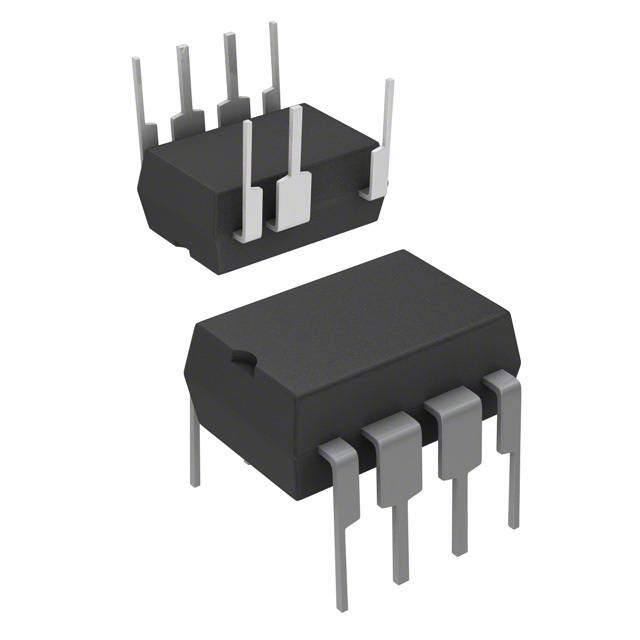
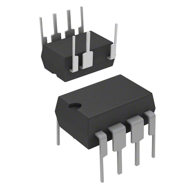
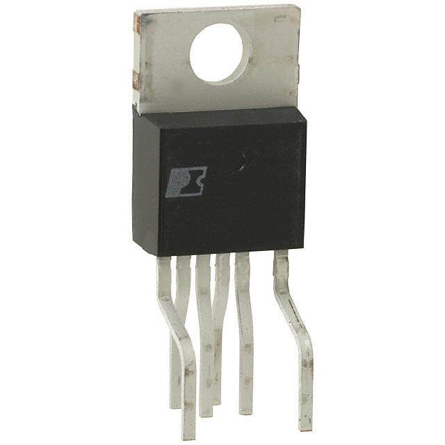
| 供应商器件封装 | DIP-8B |
| 其它名称 | 596-1029-5 |
| 功率(W) | 4W |
| 包装 | 管件 |
| 占空比-最大 | 80 % |
| 参考设计库 | http://www.digikey.com/rdl/4294959904/4294959863/35 |
| 商标 | Power Integrations |
| 安装风格 | Through Hole |
| 封装 | Tube |
| 封装/外壳 | 8-DIP(0.300",7.62mm),7 引线 |
| 封装/箱体 | DIP-8 |
| 工作温度 | -40°C ~ 150°C |
| 工作温度范围 | - 40 C to + 150 C |
| 工厂包装数量 | 50 |
| 开关频率 | 42 kHz |
| 标准包装 | 50 |
| 电压-击穿 | 700V |
| 电压-输入 | - |
| 电压-输出 | - |
| 电源电流 | 1.06 mA |
| 类型 | CV or CV/CC Switcher |
| 输入/电源电压—最大值 | 265 VAC |
| 输入/电源电压—最小值 | 85 VAC |
| 输出功率 | 3 W |
| 输出电压 | 5.6 V |
| 输出电流 | 280 mA |
| 输出端数量 | 1 Output |
| 输出隔离 | 隔离 |
| 配用 | /product-detail/zh/DAK-16A/596-1001-ND/865277 |
| 频率范围 | 24kHz ~ 49.5kHz |


- 商务部:美国ITC正式对集成电路等产品启动337调查
- 曝三星4nm工艺存在良率问题 高通将骁龙8 Gen1或转产台积电
- 太阳诱电将投资9.5亿元在常州建新厂生产MLCC 预计2023年完工
- 英特尔发布欧洲新工厂建设计划 深化IDM 2.0 战略
- 台积电先进制程称霸业界 有大客户加持明年业绩稳了
- 达到5530亿美元!SIA预计今年全球半导体销售额将创下新高
- 英特尔拟将自动驾驶子公司Mobileye上市 估值或超500亿美元
- 三星加码芯片和SET,合并消费电子和移动部门,撤换高东真等 CEO
- 三星电子宣布重大人事变动 还合并消费电子和移动部门
- 海关总署:前11个月进口集成电路产品价值2.52万亿元 增长14.8%


PDF Datasheet 数据手册内容提取
This product is not recommended for new designs. LNK500 LinkSwitch Family Energy Efficient, CV or CV/CC Switcher for Very Low Cost Chargers and Adapters Product Highlights LinkSwitch D S Cost Effective Linear/RCC Replacement C • Lowest cost and component count, constant voltage (CV) or constant voltage/constant current (CV/CC) solution Wide Range DC • Extremely simple circuit configuration HV DC Input Output • Up to 75% lighter power supply reduces shipping cost (V ) O • Primary based CV/CC solution eliminates 10 to 20 secondary components for low system cost • Combined primary clamp, feedback, IC supply, and loop compensation functions – minimizes external components (a) • Fully integrated auto-restart for short circuit and open loop Example Characteristic V V fault protection – saves external component costs O Min Typ O ±5% • 42 kHz operation simplifies EMI filter design ±10% Much Higher Performance Over Linear/RCC • Universal input range allows worldwide operation • Up to 70% reduction in power dissipation – reduces enclosure size significantly ±25%* IO ±25%* IO • CV/CC output characteristic without secondary feedback (b) For Circuit With Optional • System level thermal and current limit protection Shown Above Secondary Feedback** • Meets all single point failure requirements with only one *Estimated tolerance achievable in high volume production additional clamp capacitor including transformer and other component tolerances. • Controlled current in CC region provides inherent soft-start **See Optional Secondary Feedback section. • Optional opto feedback improves output voltage accuracy PI-3415-112202 EcoSmart™ – Extremely Energy Efficient Figure 1. Typical Application – Not a Simplified Circuit (a) and • Consumes <300 mW at 265 VAC input with no load Output Characteristic Tolerance Envelopes (b). • Meets California Energy Commission (CEC), Energy Star, and EU requirements Output Power Table1 • No current sense resistors – maximizes efficiency 230 VAC ±15% 85-265 VAC No-Load Applications Product4 Input • Linear transformer replacement in all ≤3 W applications Min2 Typ2 Min2 Typ2 Power • Chargers for cell phones, cordless phones, PDAs, digital cameras, MP3/portable audio devices, shavers, etc. LNK500 3.2 W 4 W 2.4 W 3 W <300 mW • Home appliances, white goods and consumer electronics P or G 4.3 W 5.5 W 2.9 W 3.5 W <500 mW3 • Constant output current LED lighting applications • TV standby and other auxiliary supplies Table 1. Notes: 1. Output power for designs in an enclosed adapter measured at 50 °C ambient. 2. See Figure 1 (b) for Min (CV only designs) and Typ (CV/CC charger designs) power Description points identified on output characteristic. 3. Uses higher reflected voltage transformer designs for increased power capability – see LinkSwitch™ is specifically designed to replace low power Key Application Considerations section. 4. For lead-free package linear transformer/RCC chargers and adapters at equal or options, see Part Ordering Information. lower system cost with much higher performance and energy efficiency. LNK500 is a lower cost version of the LNK501 with a wider tolerance output CC characteristic. LinkSwitch introduces consumption, a LinkSwitch solution can save the end user a revolutionary patented topology for the design of low power enough energy over a linear design to completely pay for switching power supplies that rivals the simplicity and low the full power supply cost in less than one year. LinkSwitch cost of linear adapters, and enables a much smaller, lighter, integrates a 700 V power MOSFET, PWM control, high voltage and attractive package when compared with the traditional start-up, current limit, and thermal shutdown circuitry, onto a “brick.” With efficiency of up to 75% and <300 mW no-load monolithic IC. September 2016
LNK500 DRAIN CONTROL VC 0 INTERNAL ZC 1 SUPPLY SHUTDOWN/ SHUNT REGULATOR/ AUTO-RESTART CURRENT ERROR AMPLIFIER LIMIT + ADJUST ÷ 8 - 5.6 V - 4.7 V CURRENT LIMIT + 5.7 V COMPARATOR - + IFB HYSTERETIC THERMAL SHUTDOWN OSCILLATOR DMAX CLOCK S Q SAW - R + PWM COMPARATOR IDCS LEADING EDEDGGEE LOW BLANKING RE FREQUENCY OPERATION SOURCE PI-3416-111802 Figure 2. Block Diagram. Pin Functional Description LNK500 DRAIN (D) Pin: S 1 8 C Power MOSFET drain connection. Provides internal operating current for start-up. Internal current limit sense point for drain S 2 7 S current. S 3 CONTROL (C) Pin: Error amplifier and feedback current input pin for duty cycle S 4 5 D and current limit control. Internal shunt regulator connection to provide internal bias current during normal operation. It is also P Package (DIP-8B) used as the connection point for the supply bypass and auto- restart/compensation capacitor. G Package (SMD-8B) PI-3417-111802 SOURCE (S) Pin: Figure 3. Pin Configuration. Output MOSFET source connection for high voltage power return. Primary side control circuit common and reference point. 2 Rev. E 09/16 www.power.com
LNK500 LinkSwitch Functional Description Internal Current Limit The duty cycle, current limit and operating frequency Auto-restart relationships with CONTROL pin current are shown in Figure 4. Figure 5 shows a typical power supply outline I LIM schematic which is used below to describe the LinkSwitch operation. Power Up During power up, as V is first applied (Figure 5), the CONTROL IN pin capacitor C1 is charged through a switched high voltage current source connected internally between the DRAIN and CONTROL pins (see Figure 2). When the CONTROL pin voltage reaches approximately 5.6 V relative to the SOURCE CONTROL Current IC I DCT pin, the high voltage current source is turned off, the internal control circuitry is activated and the high voltage internal Duty Cycle MOSFET starts to switch. At this point, the charge stored on C1 is used to supply the internal consumption of the chip. Auto-restart Constant Current (CC) Operation 77% As the output voltage, and therefore the reflected voltage across the primary transformer winding ramp up, the feedback CONTROL current I increases. As shown in Figure 4, the C internal current limit increases with I and reaches I when I C LIM C 30% is equal to I . The internal current limit vs. I characteristic is DCT C designed to provide an approximately constant power supply output current as the power supply output voltage rises. 3.8% I CD1 I Constant Voltage (CV) Operation CONTROL Current IC DCS When I exceeds I , typically 2 mA (Figure 4), the maximum C DCS Frequency duty cycle is reduced. At a value of I that depends on power C supply input voltage, the duty cycle control limits LinkSwitch peak current below the internal current limit value. At this point Auto-restart the power supply transitions from CC to CV operation. With f OSC minimum input voltage in a typical universal input design, this transition occurs at approximately 30% duty cycle. Resistor R1 f (Figure 5) is therefore initially selected to conduct a value of I OSC(low) C approximately equal to I when V is at the desired value DCT OUT at the minimum power supply input voltage. The final choice of R1 is made when the rest of the circuit design is complete. When the duty cycle drops below approximately 4%, the frequency is reduced, which reduces energy consumption CONTROL Current IC under light load conditions. PI-2799-112101 Auto-Restart Operation When a fault condition, such as an output short circuit or open Figure 4. CONTROL Characteristics. loop, prevents flow of an external current into the CONTROL pin, the capacitor C1 discharges towards 4.7 V. At 4.7 V, auto-restart is activated, which turns the MOSFET off and puts LinkSwitch the control circuitry in a low current fault protection mode. In D S auto-restart, LinkSwitch periodically restarts the power supply C C1 so that normal power supply operation can be restored when the fault is removed. C2 R1 C4 VOUT VIN D1 R2 D2 PI-2715-100801 Figure 5. Power Supply Outline Schematic. 3 www.power.com Rev. E 09/16
LNK500 The characteristics described above provide an approximate R3 forms a potential divider with R1 to limit the U1 collector CV/CC power supply output without the need for secondary- emitter voltage. side voltage or current feedback. The output voltage regulation is influenced by how well the voltage across C2 tracks the On the secondary side, the addition of voltage sense circuit reflected output voltage. This tracking is influenced by the value components R4, VR1 and U1 LED provide the voltage of the transformer leakage inductance which introduces an feedback signal. In the example shown, a simple Zener (VR1) error. Resistor R2 and capacitor C2 partially filter the leakage reference is used though a precision TL431 reference is inductance voltage spike reducing this error. This circuitry, used typically needed to provide ±5% output voltage tolerancing with standard transformer construction techniques provides and cable drop compensation, if required. Resistor R4 provides much better output load regulation than a linear transformer, biasing for VR1. The regulated output voltage is equal to the making this an ideal power supply solution in many low sum of the VR1 Zener voltage plus the forward voltage drop power applications. If tighter load regulation is required, an of the U1 LED. Resistor R5 is an optional low value resistor to optocoupler configuration can be used while still employing the limit U1 LED peak current due to output ripple. Manufacturer’s constant output current characteristics provided by LinkSwitch. specifications for U1 current and VR1 slope resistance should be consulted to determine whether R5 is required. Optional Secondary Feedback Figure 6 shows a typical power supply outline schematic using U1 is arranged with collector connected to primary ground and LinkSwitch with optocoupler feedback to improve output emitter to the anode of D1. This connection keeps the opto voltage regulation. On the primary side, the schematic differs in an electrically “quiet” position in the circuit. If the opto was from Figure 5 by the addition of R3, C3 and optocoupler U1. instead placed on the cathode side of D1, it would become LinkSwitch D S VOUT LNK500 C C1 R5 C2 R1 U1 85-265 R4 VAC R2 D1 VR1 U1 R3 C3 RTN PI-3418-111802 Figure 6. Power Supply Outline Schematic with Optocoupler Feedback. Output Voltage Inherent CC to CV Tolerance envelope transition without optocoupler point Voltage Typical inherent feedback characteristic without threshold optocoupler Characteristic with optocoupler Load variation during battery charging Output Current PI-2788-092101 Figure 7. Influence of the Optocoupler on the Power Supply Output Characteristic. 4 Rev. E 09/16 www.power.com
LNK500 a switching node, generating additional common mode EMI transistor voltage and dissipation ratings and should be fully currents through its internal parasitic capacitance. tested before finalizing a design. The values of C2 and C3 are less important other than to make sure they are large enough The feedback configuration in Figure 6 is simply a resistive to have very little influence on the impedance of the voltage divider made up of R1 and R3 with D1, R2, C1 and C2 division circuit set up by R1, R3 and U1 at the switching rectifying, filtering and smoothing the primary winding voltage frequency. Normally, the values of C2 and C3 in Figure 6 are signal. The optocoupler therefore effectively adjusts the resistor chosen equal to the value of C2 in Figure 5, though the voltage divider ratio to control the DC voltage across R1 and therefore, rating may be reduced depending on the relative values of R1 the feedback current received by the LinkSwitch CONTROL pin. and R2 discussed above. See Applications section for typical values of components. When the power supply operates in the constant current (CC) region, for example when charging a battery, the output voltage Figure 7 shows the influence of optocoupler feedback on the is below the voltage feedback threshold defined by U1 and output characteristic. The envelope defined by the dashed VR1 and the optocoupler is fully off. In this region, the circuit lines represent the worst case power supply DC output voltage behaves exactly as previously described with reference to and current tolerances (unit-to-unit and over the input voltage Figure 5 where the reflected voltage increases with increasing range) if an optocoupler is not used. A typical example of an output voltage and the LinkSwitch internal current limit is inherent (without optocoupler) output characteristic is shown adjusted to provide an approximate CC output characteristic. dotted. This is the characteristic that would result if U1, R4 and Note that for similar output characteristics in the CC region, the VR1 were removed. The optocoupler feedback results in the value of R1 in Figure 5 will be equal to the value of R1 + R3 in characteristic shown by the solid line. The load variation arrow Figure 6. in Figure 7 represents the locus of the output characteristic normally seen during a battery charging cycle. The two When the output reaches the voltage feedback threshold set characteristics are identical as the output voltage rises but then by U1 and VR1, the optocoupler turns on. Any further increase separate as shown when the voltage feedback threshold is in the power supply output voltage results in the U1 transistor reached. This is the characteristic seen if the voltage feedback current increasing, which increases the percentage of the threshold is above the output voltage at the inherent CC to CV reflected voltage appearing across R1. The resulting increase transition point also indicated in Figure 7. in the LinkSwitch CONTROL current reduces the duty cycle according to Figure 4 and therefore, maintains the output Figure 8 shows a case where the voltage feedback threshold voltage regulation. is set below the voltage at the inherent CC to CV transition point. In this case, as the output voltage rises, the secondary Normally, R1 and R3 are chosen to be equal in value. However, feedback circuit takes control before the inherent CC to CV increasing R3 (while reducing R1 to keep R1 + R3 constant) transition occurs. In an actual battery charging application, this increases loop gain in the CV region, improving load regulation. simply limits the output voltage to a lower value. The extent to which R3 can be increased is limited by opto Output Voltage Inherent Tolerance envelope CC to CV without optocoupler transition Typical inherent point characteristic without Voltage optocoupler V feedback O(MAX) Characteristic with threshold optocoupler Power Supply peak output power curve Load variation during battery charging Characteristic observed with load variation often applied during laboratory bench testing Output Current PI-2790-092101 Figure 8. Output Characteristic with Optocoupler Regulation (Reduced Voltage Feedback Threshold). 5 www.power.com Rev. E 09/16
LNK500 However, in laboratory bench tests, it is often more convenient The secondary of the transformer is rectified and filtered by D6 to test the power supply output characteristic starting from a and C5 to provide the DC output to the load. low output current and gradually increasing the load. In this case, the optocoupler feedback regulates the output voltage LinkSwitch dramatically simplifies the secondary side by until the peak output power curve is reached as shown in controlling both the constant voltage and constant current Figure 8. Under these conditions, the output current will regions entirely from the primary side. This is achieved by continue to rise until the peak power point is reached and monitoring the primary-side V (voltage output reflected). OR the optocoupler turns off. Once the optocoupler is off, the CONTROL pin feedback current is determined only by R1 and Diode D5 and capacitor C4 form the primary clamp network. R3 and the output current therefore folds back to the inherent This both limits the peak drain voltage due to leakage CC characteristic as shown. Since this type of load transition inductance and provides a voltage across C4, which is equal to does not normally occur in a battery charger, the output current the V plus an error due to the parasitic leakage inductance. never overshoots the inherent constant current value in the ResisOtoRr R2 filters the leakage inductance spike and reduces actual application. the error in the value of the V . Resistor R1 converts this OR voltage into a current that is fed into the CONTROL pin to In some applications it may be necessary to avoid any output regulate the output. current overshoot, independent of the direction of load variation. To achieve this goal, the minimum voltage feedback threshold During CV operation the output is regulated through control of should be set at V . This will ensure that the voltage at the duty cycle. As the current into the CONTROL pin exceeds O(MAX) the CC to CV transition point of the inherent characteristic will approximately 2 mA, the duty cycle begins to reduce, reaching always occur below the voltage feedback threshold. However, 30% at a CONTROL pin current of 2.3 mA. the output voltage tolerance is then increased, since the inherent CV characteristic tolerance below V is added to O(MAX) Under light or no-load conditions, when the duty cycle reaches the tolerance of the optocoupler feedback circuit. approximately 4%, the switching frequency is reduced to lower energy consumption. Applications Example If the output load is increased beyond the peak power point The circuit shown in Figure 9 shows a typical implementation (defined by 0.5·L ·I 2·f), the output voltage and V falls. of an approximate constant voltage / constant current (CV/CC) The reduced CONPTLIRMOL pin current will lower the OinRternal charger using LinkSwitch. This design delivers 2.75 W with a LinkSwitch current limit (current limit control) providing an nominal peak power point voltage of 5.5 V and a current of approximately constant current output characteristic. If the 500 mA. Efficiency is greater than 70% over an input range of load is increased and the CONTROL pin current falls below 85 VAC to 265 VAC. approximately 1 mA, the CONTROL pin capacitor C3 will discharge and the supply enters auto-restart. The bridge rectifier, BR1, rectifies the AC input. Resistor, RF1 is a fusible type providing protection from primary-side short Current limit control removes the need for any secondary circuits. The rectified AC is smoothed by C1 and C2 with side current sensing components (sense resistor, transistor, inductor L1 forming a pi-filter in conjunction with C1 and C2 to opto coupler and associated components). Removing the filter conducted EMI. The switching frequency of 42 kHz allows secondary sense circuit dramatically improves efficiency, giving such a simple EMI filter to be used without the need for a the associated benefit of reduced enclosure size. Y capacitor while still meeting international EMI standards. Key Application Considerations When power is applied, high voltage DC appears at the DRAIN pin of LinkSwitch (U1). The CONTROL pin capacitor C3 is Design Output Power then charged through a switched high voltage current source connected internally between the DRAIN and CONTROL pins. Table 1 (front page) provides guidance for the maximum When the CONTROL pin reaches approximately 5.6 V relative continuous output power from a given device under the to the SOURCE pin, the internal current source is turned off. conditions specified. The internal control circuitry is activated and the high voltage MOSFET starts to switch, using the energy in C3 to power the IC. The output of chargers (CV/CC) are normally specified at the typical output peak power point. Conversely, non-charger When the MOSFET is on, the high voltage DC bus is connected applications (CV only, which applies to many converters such to one end of the transformer primary, the other end being as adapters, standby/auxiliary supplies and other embedded connected to primary return. As the current ramps in the AC-DC converters) where CC operation is not required, are primary of flyback transformer T1, energy is stored. This normally specified at the minimum output power they will energy is delivered to the output when the MOSFET turns off supply under worst-case conditions. each switching cycle. 6 Rev. E 09/16 www.power.com
LNK500 U1 LNK500 L1 LinkSwitch 1 mH T1 D S 1 5 5.5 V, 500 mA C3 C BR1 0 . 2520 VF # 3141 6A WTG 4 # 3 105 A TWG 4 7 C0 5F RF1 1 A, 600 V R1 C4 TIW 10 V 10 1 W 20.5 k 0.1 F Fusible 1% 100 V RTN 3 6 C1 C2 D6 85-265 4.7 F 4.7 F 11DQ06 VAC 400 V 400 V D5 EE13 1N4937 LP = 2.55 mH R2 100 PERFORMANCE SUMMARY Output Power: 2.75 W Efficiency: 72% No Load Consumption: 260 mW, 230 VAC 200 mW, 115 VAC PI-3419-111802 Figure 9. 2.75 W Constant Voltage/Constant Current (CV/CC) Charger using LinkSwitch. 190 VVIINN == 8151 5V VAACC PI-3420-111802 8 VIN = 185 VAC VIN = 265 VAC V) 7 ,T U O 6 V ( e g 5 a t ol V 4 t u p ut 3 O 2 1 0 0 100 200 300 400 500 600 700 Output Current (IOUT, mA) Figure 10. Measured Output Characteristic of the Circuit in Figure 9. 7 www.power.com Rev. E 09/16
LNK500 To aid the designer, the power table reflects these differences. an estimated overall constant current tolerance of ±25% the For CV/CC designs the typical power column and for CV primary inductance tolerance should be ±10% or better. This designs the minimum power column should be used, is achievable using standard low cost, center leg gapping respectively. Additionally, figures are based on the following techniques where the gap size is typically 0.08 mm or larger. conditions: Smaller gap sizes are possible but require non-standard, tighter ferrite A tolerances. L 1. The minimum DC input bus voltage is 90 V or higher. This corresponds to a filter capacitor of 3 µF/W for universal Other gapping techniques such as film gapping allow tighter input and 1 µF/W for 230 VAC or 115 VAC input with tolerances (±7% or better) with associated improvements in doubler input stage. the tolerance of the peak power point. Please consult your 2. Design is a discontinuous mode flyback converter. transformer vendor for guidance. Continuous mode designs can result in loop instability and are therefore not recommended. For typical output power Core gaps should be uniform. Uneven core gapping, especially figures, nominal values for primary inductance and I2f are with small gap sizes, may cause variation in the primary assumed. For minimum output power figures, primary inductance with flux density (partial saturation) and make the inductance minus 10% and the minimum I2f value are constant current region non-linear. To verify uniform gapping assumed. For no-load consumption <300 mW, a V in the it is recommended that the primary current wave-shape be OR range 40 V to 60 V is assumed. For no-load consumption examined while feeding the supply from a DC source. The <500 mW and higher output power capability, a V in the gradient is defined as di/dt = V/L and should remain constant OR range 60 V to 100 V is assumed. throughout the MOSFET on time. Any change in gradient of 3. A secondary output of 5 V with a Schottky rectifier diode. the current ramp is an indication of uneven gapping. 4. Assumed efficiency of 70%. 5. The part is board mounted with SOURCE pins soldered to Measurements made using an LCR bridge should not be sufficient area of copper to keep the die temperature at or solely relied upon; typically these instruments only measure at below 100 °C. currents of a few milliamps. This is insufficient to generate high 6. An output cable with a total resistance of 0.2 Ω. enough flux densities in the core to show uneven gapping. In addition to the thermal environment (sealed enclosure, For a typical EE13 core using center leg gapping, a 0.08 mm ventilated, open frame, etc), the maximum power capability gap (A of 190 nH/t2) allows a primary inductance tolerance of of LinkSwitch in a given application depends on transformer LG ±10% to be maintained in standard high volume production. core size, efficiency, primary inductance tolerance, minimum This allows the EE13 to be used in designs up to 2.75 W with specified input voltage, input storage capacitance, output less than 300 mW no-load consumption. If film gapping is voltage, output diode forward drop, etc., and can be different used then this increases to 3 W. Moving to a larger core, EE16 from the values shown in Table 1. for example, allows a 3 W output with center leg gapping. Transformer Design The transformer turns ratio should be selected to give a V To provide an approximately CV/CC output, the transformer OR (output voltage reflected through secondary to primary turns should be designed to be discontinuous; all the energy stored ratio) of 40 V to 60 V. In designs not required to meet 300 mW in the transformer is transferred to the secondary during the no-load consumption targets, the transformer can be designed MOSFET off time. Energy transfer in discontinuous mode is with higher V as long as discontinuous mode operation is independent of line voltage. OR maintained. This increases the output power capability. For example, a 230 VAC input design using an EE19 transformer The peak power point prior to entering constant current core with V >70 V, is capable of delivering up to 5.5 W typical operation is defined by the maximum power transferred by the OR output power. Note: the linearity of the CC region of the power transformer. The power transferred is given by the expression supply output characteristic is influenced by V . If this is an P = 0.5·L ·I2·f, where L is the primary inductance, I2 is the OR P P important aspect of the application, the output characteristic primary peak current squared and f is the switching frequency. should be checked before finalizing the design. To simplify analysis, the data sheet parameter table specifies an Output Characteristic Variation I2f coefficient. This is the product of current limit squared and Both the device tolerance and external circuit govern the overall switching frequency normalized to the feedback parameter I . tolerance of the LinkSwitch output characteristic. Estimated DCT This provides a single term that specifies the variation of the peak power point tolerances for a 3 W design are ±10% for peak power point in the power supply due to LinkSwitch. voltage and ±25% for current limit for overall variation in high volume manufacturing. This includes device and transformer As primary inductance tolerance is part of the expression tolerances and line variation. Lower power designs may have that determines the peak output power point (start of the CC poorer constant current linearity. characteristic) this parameter should be well controlled. For 8 Rev. E 09/16 www.power.com
LNK500 As the output load reduces from the peak power point, the Feedback Resistor – R1 output voltage will tend to rise due to tracking errors compared The value of R1 is selected to give a feedback current into the to the load terminals. Sources of these errors include the CONTROL pin of approximately 2.3 mA at the peak output output cable drop, output diode forward voltage and leakage power point of the supply. The actual value depends on the inductance, which is the dominant cause. As the load reduces, V selected during design. Any 0.25 W resistor is suitable. OR the primary operating peak current reduces, together with the leakage inductance energy, which reduces the peak charging Output Diode – D2 of the clamp capacitor. With a primary leakage inductance of Either PN fast, PN ultra-fast or Schottky diodes can be used, 50 µH, the output voltage typically rises 30% over a 100% to depending on the efficiency target for the supply, Schottky 5% load change. diodes giving higher efficiency then PN diodes. The diode voltage rating should be sufficient to withstand the output At very light or no-load, typically less than 2 mA of output voltage plus the input voltage transformed through the turns current, the output voltage rises due to leakage inductance ratio (a typical V of 50 V requires a diode PIV of 50 V). OR peak charging of the secondary. This voltage rise can be Slow recovery diodes are not recommended (1N400X types). reduced with a small preload with little change to no-load Output Capacitor – C4 power consumption. Capacitor C4 should be selected such that its voltage and ripple current specifications are not exceeded. The output voltage load variation can be improved across the whole load range by adding an optocoupler and secondary LinkSwitch Layout considerations reference (Figure 6). The secondary reference is designed to only provide feedback above the normal peak power point Primary-Side Connections voltage to maintain the correct constant current characteristic. Since the SOURCE pins in a LinkSwitch supply are switching nodes, the copper area connected to SOURCE together with Component Selection C1, C2 and R1 (Figure 5) should be minimized, within the ther- mal contraints of the design, to reduce EMI coupling. The schematic shown in Figure 5 outlines the key components needed for a LinkSwitch supply. The CONTROL pin capacitor C1 should be located as close as possible to the SOURCE and CONTROL pins. Clamp diode – D1 Diode D1 should be either a fast (t <250 ns) or ultra-fast rr To minimize EMI coupling from the switching nodes on the type (t <50 ns), with a voltage rating of 600 V or higher. Fast rr primary to both the secondary and AC input, the LinkSwitch recovery types are preferred, being typically lower cost. Slow should be positioned away from the secondary of the diodes are not recommended; they can allow excessive DRAIN transformer and AC input. ringing and the LinkSwitch to be reverse biased. Clamp Capacitor – C2 Routing the primary return trace from the transformer primary Capacitor C2 should be a 0.1 µF, 100 V capacitor. Low cost around LinkSwitch and associated components further reduces metallized plastic film types are recommended. The tolerance coupling. of this part has a very minor effect on the output characteristic Y Capacitor so any of the standard ±5%, ±10% or ±20% tolerances are If a Y capacitor is required, it should be connected close to the acceptable. Ceramic capacitors are not recommended. The transformer secondary output return pin(s) and the primary bulk common dielectrics used such as Y5U or Z5U are not stable capacitor negative return. Such placement will maximize the with voltage or temperature and may cause output instability. EMI benefit of the Y capacitor and avoid problems in common- Ceramic capacitors with high stability dielectrics may be used mode surge testing. but are expensive compared to metallized film types. CONTROL Pin Capacitor – C1 Capacitor C1 is used during start-up to power LinkSwitch and sets the auto-restart frequency. For designs that have a battery load, this component should have a value of 0.22 µF and for resistive loads, a value of 1 µF. This ensures there is sufficient time during start-up for the output voltage to reach regulation. Any capacitor type is acceptable with a voltage rating of 10 V or above. 9 www.power.com Rev. E 09/16
LNK500 Quick Design Checklist 3. Thermal check – At peak output power, minimum input voltage and maximum ambient temperature, verify that the As with any power supply design, all LinkSwitch designs temperature specifications are not exceeded for LinkSwitch, should be verified on the bench to make sure that component transformer, output diode and output capacitors. Enough specifications are not exceeded under worst case conditions. thermal margin should be allowed for part-to-part variation Note: In a LinkSwitch circuit, the SOURCE is a switching of the R of LinkSwitch as specified in the data sheet. DS(ON) node. This should be taken into consideration during testing. Under low line, peak power, a maximum LinkSwitch Oscilloscope measurements should be made with probe SOURCE pin temperature of 100 °C is recommended to grounded to DC voltages such as primary return or DC rail but allow for these variations. not to SOURCE. Power supply input voltage should always be supplied using an isolation transformer. The following minimum 4. Centered output characteristic – Using a transformer with set of tests is strongly recommended: nominal primary inductance and at an input voltage midway between low and high line, verify that the peak power point occurs at the desired nominal output current, with 1. Maximum drain voltage – Verify that V does not exceed DS the correct output voltage. If this does not occur then the 675 V at highest input voltage and peak output power. design should be refined to ensure the overall tolerance limits are met. 2. Maximum drain current – At maximum ambient temperature, maximum input voltage and peak output power, verify drain current waveforms at start-up for any Design Tools signs of transformer saturation and excessive leading edge current spikes. LinkSwitch has a minimum leading edge Up-to-date information on design tools can be found at the blanking time of 200 ns to prevent premature termination Power Integrations website: www.power.com. of the on-cycle. Verify that the leading edge current spike event is below current limit at the end of the 200 ns blanking period. Input Filter Capacitor C S D + LinkSwitch HV DC Input - Transformer S S S S Y1- Capacitor - DC Out + PI-2900-070202 Output Capacitor Figure 11. Recommended Circuit Board Layout for LinkSwitch using P Package. 10 Rev. E 09/16 www.power.com
LNK500 ABSOLUTE MAXIMUM RATINGS(1,4) DRAIN Voltage ...................................................-0.3 V to 700 V Notes: DRAIN Peak Current .....................................................400 mA 1. All voltages referenced to SOURCE, T = 25 °C. A CONTROL Voltage ................................................ -0.3 V to 9 V 2. Normally limited by internal circuitry. CONTROL Current (not to exceed 9 V) .........................100 mA 3. 1/16 in. from case for 5 seconds. Storage Temperature .....................................-65 °C to 150 °C 4. Maximum ratings specified may be applied, one at a time, Operating Junction Temperature(2) ..................-40 °C to 150 °C without causing permanent damage to the product. Lead Temperature(3) .........................................................260 °C Exposure to Absolute Maximum Rating conditions for extended periods of time may affect product reliability. THERMAL IMPEDANCE Thermal Impedance: P or G Package: Notes: (q ) ...............................70 °C/W(2); 55 °C/W(3) 1. Measured on pin 2 (SOURCE) close to plastic interface. JA (q )(1) ...............................................11 °C/W 2. Soldered to 0.36 sq. in. (232 mm2), 2 oz. (610 g/m2) copper clad. JC 3. Soldered to 1 sq. in. (645 mm2), 2 oz. (610 g/m2) copper clad. Conditions SOURCE = 0 V; T = -40 to 125 °C Parameter Symbol J Min Typ Max Units See Figure 12 (Unless Otherwise Specified) CONTROL FUNCTIONS Switching f I = I , T = 25 °C 34.5 42 49.5 kHz Frequency OSC C DCT J Low Switching Duty Cycle = DC f LF 24 30 36 kHz Frequency OSC(LOW) T = 25 °C J Duty Cycle at Low Frequency Switching from f to f , Switching DC OSC OSC(LOW) 2.4 3.8 5.2 % LF T = 25 °C Frequency J Low Frequency DC Frequency = f , T = 25 °C 1.8 3.15 4.5 % Duty Cycle Range (RANGE) OSC(LOW) J Maximum Duty DC I = 1.5 mA 74 77 80 % Cycle MAX C PWM Gain DC I = I , T = 25 °C -0.45 -0.35 -0.25 %/µA REG C DCT J CONTROL Pin T = 25 °C Current at 30% I J 2.21 2.30 2.39 mA DCT See Figure 4 Duty Cycle CONTROL Pin V I = I 5.5 5.75 6 V Voltage C(IDCT) C DCT Dynamic Z I = I ,T = 25 °C 60 90 120 Ω Impedance C C DCT J 11 www.power.com Rev. E 09/16
LNK500 Conditions SOURCE = 0 V; T = -40 to 125 °C Parameter Symbol J Min Typ Max Units See Figure 12 (Unless Otherwise Specified) SHUTDOWN/AUTO-RESTART CONTROL Pin V = 0 V -4.5 -3.25 -2 C I T = 25 °C mA Charging Current C(CH) J V = 5.15 V -2.3 -1.3 -0.3 C Control/Supply/ I T = 25 °C Output MOSFET Enabled 0.95 1.06 1.14 CD1 J mA Discharge Current I T = 25 °C Output MOSFET Disabled 0.7 0.9 1.1 CD2 J Auto-Restart V 5.6 V Threshold Voltage C(AR) Auto-Restart V 0.9 V Hysteresis Voltage C(AR)hyst Auto-Restart Duty Short Circuit Applied at DC 8 % Cycle (AR) Power Supply Output Auto-Restart S2 Open f 300 Hz Frequency (AR) C1 = 0.22 µF (See Figure 12) CIRCUIT PROTECTION Self-Protection T = 25 °C J I di/dt = 90 mA/µs 228 254 280 mA Current Limit LIM See Note C T = 25 °C J I2 f Coefficient I2 f di/dt = 90 mA/µs 2412 2710 3008 A2Hz See Notes C, D Current Limit at I I = I ,T = 25 °C 158 mA Auto-Restart LIM(AR) C CD1 J Power Up Reset V 1.5 2.75 4.0 V Threshold Voltage C(RESET) Leading Edge t I = I ,T = 25 °C 200 300 ns Blanking Time LEB C DCT J Current Limit Delay t T = 25 °C 100 ns IL(D) J Thermal Shutdown I =I 125 135 °C Temperature C DCT Thermal Shutdown 70 °C Hysteresis 12 Rev. E 09/16 www.power.com
LNK500 Conditions SOURCE = 0 V; T = -40 to 125 °C Parameter Symbol J Min Typ Max Units See Figure 12 (Unless Otherwise Specified) OUTPUT ON-State T = 25 °C 28 32 J R I = 25 mA Ω Resistance DS(ON) D T = 100 °C 42 48 J OFF-State Drain V = 6.2 V I C 50 µA Leakage Current DSS V = 560 V, T = 125 °C D A See Note B Breakdown Voltage BV 700 V DSS V = 6.2 V, T = 25 °C C A DRAIN Supply See Note E 36 50 V Voltage NOTES: A. For specifications with negative values, a negative temperature coefficient corresponds to an increase in magnitude with increasing temperature, and a positive temperature coefficient corresponds to a decrease in magnitude with increasing temperature. B. Breakdown voltage may be checked against minimum BV specification by ramping the DRAIN pin voltage up to but not DSS exceeding minimum BV . DSS C. I is increased gradually to obtain maximum current limit at di/dt of 90 mA/µs. Increasing I further would terminate the cycle C C through duty cycle control. D. This parameter is normalized to I to correlate to power supply output current (it is multiplied by I (nominal)/I ). DCT DCT DCT E. It is possible to start up and operate LinkSwitch at DRAIN voltages well below 36 V. However, the CONTROL pin charging current is reduced, which affects start-up time, auto-restart frequency, and auto-restart duty cycle. Refer to the characteristic graph on CONTROL pin charge current (I ) vs. DRAIN voltage (Figure 13) for low voltage operation characteristics. C 13 www.power.com Rev. E 09/16
LNK500 750 Ω LinkSwitch D S S1 S 10 kΩ S S C S S2 40 V 40 V 0.22 µF PI-2894-062802 Figure 12. LinkSwitch General Test Circuit. mA)12.6 VC = 5.15 V PI-2901-071602 t2 Pinnt ( t1 OL rre1.2 HV90% 90% u RC CONTrging 0.8 VDORLTAAINGE D = tt1 a 2 h C0.4 10% 0 V 0 0 20 40 60 80 100 PI-2048-021015 DRAIN Voltage (V) Figure 14. Duty Cycle Measurement. Figure 13. I vs. DRAIN Voltage. C mA)112000 PI-2895-062802 978000 PI-2902-071602 nt ( 80 %) 60 Curre 60 ycle ( 50 n C 40 Pi y ol 40 Dut 30 r t on 20 C 20 10 0 0 0.0 2.0 4.0 6.0 8.0 10.0 12.0 14.0 2.15 2.25 2.35 2.45 2.55 2.65 Control Pin Voltage (V) Control Pin Current (mA) Figure 15. CONTROL Pin I-V Characteristic. Figure 16. Duty Cycle vs. CONTROL Pin Current. 14 Rev. E 09/16 www.power.com
LNK500 Typical Performance Characteristics Voltageo 25 C)°1.1 PI-2213-012301 equencyor 25 C)° 110...208000000 PI-2896-062802 wn ed t1.0 g Fred f 0.600 reakdoormaliz witchinormaliz 0.400 BN SN ( ( 0.200 0.9 0.000 -50 -25 0 25 50 75 100 125 150 -50 0 50 100 150 Junction Temperature (°C) Junction Temperature (°C) Figure 17. Breakdown Voltage vs. Temperature. Figure 18. Switching Frequency vs. Temperature. C) 11..200000 PI-2897-062802 C)11..20 PI-2910-071602 nt Limited for 25 ° 00..860000 efficiented for 25 °00..86 ez oz Currmali 0.400 2f Cmali0.4 or Ior N N ( 0.200 (0.2 0.000 0.0 -50 -25 0 25 50 75 100 125 150 -50 -25 0 25 50 75 100 125 150 Junction Temperature (°C) Junction Temperature (°C) Figure 19. Current Limit vs. Temperature. Figure 20. I2f Coefficient vs. Temperature. 25 C)° 11..200000 PI-2898-062802 or 25 C)° 1.21 PI-2899-062802 or 0.800 d f 0.8 ed f alize z 0.600 m 0.6 ali r m o N Nor 0.400 n ( 0.4 (T Gai DC 0.200 M 0.2 I W P 0.000 0 -50 0 50 100 150 -50 0 50 100 150 Junction Temperature (°C) Temperature (°C) Figure 21. I vs. Temperature. Figure 22. PWM Gain vs. Temperature. DCT 15 www.power.com Rev. E 09/16
LNK500 Typical Performance Characteristics (cont.) A) 320500 TTCCAASSEE == 2150 0° C°C PI-2222-031401 m 200 t ( n e rr 150 u C n ai 100 r D 50 0 0 2 4 6 8 10 Drain Voltage (V) Figure 23. Output Characteristics (DRAIN Current vs. DRAIN Voltage). 16 Rev. E 09/16 www.power.com
LNK500 PDIP-8B (P Package) ⊕D S .004 (.10) .137 (3.48) Notes: -E- MINIMUM 1. Package dimensions conform to JEDEC specification MS-001-AB (Issue B 7/85) for standard dual-in-line (DIP) package with .300 inch row spacing. 2. Controlling dimensions are inches. Millimeter sizes are shown in parentheses. 3. Dimensions shown do not include mold flash or other .240 (6.10) protrusions. Mold flash or protrusions shall not exceed .260 (6.60) .006 (.15) on any side. 4. Pin locations start with Pin 1, and continue counter-clock- wise to Pin 8 when viewed from the top. The notch and/or dimple are aids in locating Pin 1. Pin 6 is omitted. 5. Minimum metal to metal spacing at the package body for the omitted lead location is .137 inch (3.48 mm). Pin 1 6. Lead width measured at package body. 7. Lead spacing measured with the leads constrained to be .356 (9.05) perpendicular to plane T. -D- .387 (9.83) .057 (1.45) .068 (1.73) (NOTE 6) .125 (3.18) .015 (.38) .145 (3.68) MINIMUM -T- SEATING .008 (.20) PLANE .118 (3.00) .015 (.38) .140 (3.56) .300 (7.62) BSC .100 (2.54) BSC .048 (1.22) (NOTE 7) .053 (1.35) P08B .014 (.36) .300 (7.62) .022 (.56) ⊕T E D S .010 (.25) M .390 (9.91) PI-2551-081716 17 www.power.com Rev. E 09/16
LNK500 SMD-8B (G Package) ⊕D S.004 (.10) .137 (3.48) Notes: MINIMUM 1. Controlling dimensions are inches. Millimeter sizes are -E- shown in parentheses. 2. Dimensions shown do not include mold flash or other protrusions. Mold flash or protrusions shall not exceed .420 .006 (.15) on any side. .240 (6.10) .372 (9.45) 3. Pin locations start with Pin 1, .260 (6.60) .388 (9.86) and continue counter-clock- ⊕E S.010 (.25) .046.060 .060.046 wise to Pin 8 when viewed from the top. Pin 6 is omitted. 4. Minimum metal to metal .080 spacing at the package body Pin 1 for the omitted lead location is .137 inch (3.48 mm). Pin 1 .086 5. Lead width measured at .186 package body. .100 (2.54) (BSC) .286 6. D and E are referenced datums on the package body. Solder Pad Dimensions .356 (9.05) -D- .387 (9.83) .057 (1.45) .125 (3.18) .068 (1.73) .145 (3.68) (NOTE 5) .004 (.10) .032 (.81) .048 (1.22) .037 (.94) .053 (1.35) .009 (.23) .004 (.10) .036 (0.91) 0 °-8° .012 (.30) .044 (1.12) G08B PI-2546-081716 Part Ordering Information • LinkSwitch Product Family • Series Number • Package Identifier G Plastic Surface Mount DIP P Plastic DIP • Lead Finish Blank Standard (Sn Pb) N Pure Matte Tin (Pb-Free) • Tape & Reel and Other Options Blank Standard Configurations TL Tape & Reel, 1 k pcs minimum, G Package only. LNK 500 G N - TL 18 Rev. E 09/16 www.power.com
LNK500 Notes 19 www.power.com Rev. E 09/16
LNK500 Revision Notes Date B Released Final Data Sheet. 3/03 C Added lead-free ordering information. 12/04 D Minor error and formatting corrections. 2/05 E Updated PDIP-8B (P Package) and SMD-8B (G Package) per PCN-16232. 09/16 For the latest updates, visit our website: www.power.com Power Integrations reserves the right to make changes to its products at any time to improve reliability or manufacturability. Power Integrations does not assume any liability arising from the use of any device or circuit described herein. POWER INTEGRATIONS MAKES NO WARRANTY HEREIN AND SPECIFICALLY DISCLAIMS ALL WARRANTIES INCLUDING, WITHOUT LIMITATION, THE IMPLIED WARRANTIES OF MERCHANTABILITY, FITNESS FOR A PARTICULAR PURPOSE, AND NON-INFRINGEMENT OF THIRD PARTY RIGHTS. Patent Information The products and applications illustrated herein (including transformer construction and circuits external to the products) may be covered by one or more U.S. and foreign patents, or potentially by pending U.S. and foreign patent applications assigned to Power Integrations. A complete list of Power Integrations patents may be found at www.power.com. Power Integrations grants its customers a license under certain patent rights as set forth at http://www.power.com/ip.htm. Life Support Policy POWER INTEGRATIONS PRODUCTS ARE NOT AUTHORIZED FOR USE AS CRITICAL COMPONENTS IN LIFE SUPPORT DEVICES OR SYSTEMS WITHOUT THE EXPRESS WRITTEN APPROVAL OF THE PRESIDENT OF POWER INTEGRATIONS. As used herein: 1. A Life support device or system is one which, (i) is intended for surgical implant into the body, or (ii) supports or sustains life, and (iii) whose failure to perform, when properly used in accordance with instructions for use, can be reasonably expected to result in significant injury or death to the user. 2. A critical component is any component of a life support device or system whose failure to perform can be reasonably expected to cause the failure of the life support device or system, or to affect its safety or effectiveness. The PI logo, TOPSwitch, TinySwitch, SENZero, SCALE-iDriver, Qspeed, PeakSwitch, LYTSwitch, LinkZero, LinkSwitch, InnoSwitch, HiperTFS, HiperPFS, HiperLCS, DPA-Switch, CAPZero, Clampless, EcoSmart, E-Shield, Filterfuse, FluxLink, StakFET, PI Expert and PI FACTS are trademarks of Power Integrations, Inc. Other trademarks are property of their respective companies. ©2016, Power Integrations, Inc. Power Integrations Worldwide Sales Support Locations World Headquarters Germany Italy Singapore 5245 Hellyer Avenue Lindwurmstrasse 114 Via Milanese 20, 3rd. Fl. 51 Newton Road San Jose, CA 95138, USA. 80337 Munich 20099 Sesto San Giovanni (MI) #19-01/05 Goldhill Plaza Main: +1-408-414-9200 Germany Italy Singapore, 308900 Customer Service: Phone: +49-895-527-39110 Phone: +39-024-550-8701 Phone: +65-6358-2160 Phone: +1-408-414-9665 Fax: +49-895-527-39200 Fax: +39-028-928-6009 Fax: +65-6358-2015 Fax: +1-408-414-9765 e-mail: eurosales@power.com e-mail: eurosales@power.com e-mail: singaporesales@power.com e-mail: usasales@power.com Germany Japan Taiwan China (Shanghai) HellwegForum 1 Kosei Dai-3 Bldg. 5F, No. 318, Nei Hu Rd., Sec. 1 Rm 2410, Charity Plaza, No. 88 59469 Ense 2-12-11, Shin-Yokohama, Nei Hu Dist. North Caoxi Road Germany Kohoku-ku Taipei 11493, Taiwan R.O.C. Shanghai, PRC 200030 Tel: +49-2938-64-39990 Yokohama-shi, Kanagawa Phone: +886-2-2659-4570 Phone: +86-21-6354-6323 e-mail: igbt-driver.sales@ 222-0033 Japan Fax: +886-2-2659-4550 Fax: +86-21-6354-6325 power.com Phone: +81-45-471-1021 e-mail: taiwansales@power.com e-mail: chinasales@power.com Fax: +81-45-471-3717 India UK e-mail: japansales@power.com China (Shenzhen) #1, 14th Main Road Cambridge Semiconductor, 17/F, Hivac Building, No. 2, Keji Vasanthanagar Korea a Power Integrations company Nan 8th Road, Nanshan District, Bangalore-560052 India RM 602, 6FL Westbrook Centre, Block 5, Shenzhen, China, 518057 Phone: +91-80-4113-8020 Korea City Air Terminal B/D, 159-6 2nd Floor Phone: +86-755-8672-8689 Fax: +91-80-4113-8023 Samsung-Dong, Kangnam-Gu, Milton Road Fax: +86-755-8672-8690 e-mail: indiasales@power.com Seoul, 135-728, Korea Cambridge CB4 1YG e-mail: chinasales@power.com Phone: +82-2-2016-6610 Phone: +44 (0) 1223-446483 Fax: +82-2-2016-6630 e-mail: eurosales@power.com e-mail: koreasales@power.com
Mouser Electronics Authorized Distributor Click to View Pricing, Inventory, Delivery & Lifecycle Information: P ower Integrations: LNK500PN LNK500GN LNK500GN-TL