 Datasheet下载
- 型号: DLP3000FQB
- 制造商: Texas Instruments
- 库位|库存: xxxx|xxxx
- 要求:
| 数量阶梯 | 香港交货 | 国内含税 |
| +xxxx | $xxxx | ¥xxxx |
查看当月历史价格
查看今年历史价格
DLP3000FQB产品简介:
ICGOO电子元器件商城为您提供DLP3000FQB由Texas Instruments设计生产,在icgoo商城现货销售,并且可以通过原厂、代理商等渠道进行代购。 DLP3000FQB价格参考。Texas InstrumentsDLP3000FQB封装/规格:专用 IC, Digital Micromirror Device (DMD) 50-LCCC。您可以下载DLP3000FQB参考资料、Datasheet数据手册功能说明书,资料中有DLP3000FQB 详细功能的应用电路图电压和使用方法及教程。
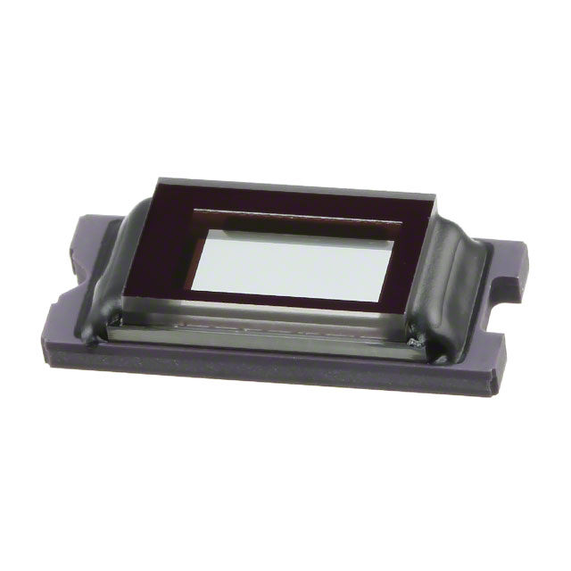
DLP3000FQB是德州仪器(Texas Instruments)推出的一款数字微镜器件(DMD),属于专用IC类别,主要用于DLP(Digital Light Processing)显示和光控制技术。该芯片广泛应用于需要高精度光图案投射的场景。

典型应用场景包括:
1. 3D打印与光固化:在SLA(立体光刻)和DLP 3D打印机中,DLP3000FQB用于高速投影切片图像,实现高分辨率、高精度的逐层成型,提升打印速度与细节表现。
2. 机器视觉与结构光扫描:用于工业三维扫描设备,通过投射编码光图案,结合摄像头捕捉物体表面形变,实现快速、精准的三维建模,适用于逆向工程、质量检测等领域。
3. 增强现实(AR)与抬头显示(HUD):在部分近眼显示或车载HUD系统中,作为微型显示核心组件,提供明亮、清晰的图像投射。
4. 医疗成像与显微设备:用于共聚焦显微镜或荧光成像系统,实现对样本的可编程照明与高速图像采集。
5. 工业光刻与激光加工:在PCB曝光、微细加工等工艺中,实现非接触式、高分辨率的图形化处理。

DLP3000FQB具备XGA级分辨率(1024×768)、高反射率铝镜阵列和快速切换能力(微秒级响应),支持灵活的时序控制,适合对光精度和速度要求高的应用。其小型化封装也便于集成到紧凑型光学系统中。
| 参数 | 数值 |
| 产品目录 | 集成电路 (IC)半导体 |
| 描述 | IC DLP 0.3 WVGA DMD 50LCCC显示驱动器和控制器 DLP 0.3 WVGA DMD |
| 产品分类 | |
| 品牌 | Texas Instruments |
| 产品手册 | http://www.ti.com/lit/gpn/dlp3000 |
| 产品图片 | |
| rohs | 符合RoHS无铅 / 符合限制有害物质指令(RoHS)规范要求 |
| 产品系列 | 驱动器IC,显示驱动器和控制器,Texas Instruments DLP3000FQB- |
| 数据手册 | |
| 产品型号 | DLP3000FQB |
| 产品 | Driver |
| 产品种类 | 显示驱动器和控制器 |
| 供应商器件封装 | 50-LCCC |
| 其它名称 | 296-30917 |
| 包装 | 散装 |
| 商标 | Texas Instruments |
| 安装类型 | 表面贴装 |
| 安装风格 | SMD/SMT |
| 封装/外壳 | 模块 |
| 封装/箱体 | LCCC-50 |
| 工厂包装数量 | 10 |
| 应用 | 3D,医疗成像 |
| 最大工作温度 | + 80 C |
| 最小工作温度 | - 40 C |
| 标准包装 | 10 |
| 电源电压 | - 0.5 V to + 4 V |
| 类型 | 数字微镜芯片(DMD) |
| 系列 | DLP3000 |


- 商务部:美国ITC正式对集成电路等产品启动337调查
- 曝三星4nm工艺存在良率问题 高通将骁龙8 Gen1或转产台积电
- 太阳诱电将投资9.5亿元在常州建新厂生产MLCC 预计2023年完工
- 英特尔发布欧洲新工厂建设计划 深化IDM 2.0 战略
- 台积电先进制程称霸业界 有大客户加持明年业绩稳了
- 达到5530亿美元!SIA预计今年全球半导体销售额将创下新高
- 英特尔拟将自动驾驶子公司Mobileye上市 估值或超500亿美元
- 三星加码芯片和SET,合并消费电子和移动部门,撤换高东真等 CEO
- 三星电子宣布重大人事变动 还合并消费电子和移动部门
- 海关总署:前11个月进口集成电路产品价值2.52万亿元 增长14.8%


PDF Datasheet 数据手册内容提取
Product Sample & Technical Tools & Support & Folder Buy Documents Software Community DLP3000 DLPS022B–JANUARY2012–REVISEDMARCH2015 ® DLP3000 DLP 0.3 WVGA Series 220 DMD 1 Features 3 Description • 0.3-Inch(7.62mm)DiagonalMicromirrorArray The DLP3000 digital micromirror device (DMD) is a 1 digitally-controlled micro-opto-electromechanical – 608 ×684ArrayofAluminum,Micrometer- system (MOEMS) spatial light modulator (SLM) SizedMirrorsOfferinguptoWVGAResolution optimized for small form-factor applications. When (854×480)WideAspectRatioDisplay coupled to an appropriate optical system, the – 7.6-µmMicromirrorPitch DLP3000 can be used to modulate the amplitude and direction of incoming light. The DLP3000 creates – ±12° MicromirrorTiltAngle(RelativetoFlat highlyflexiblelightpatternswithspeed,precision,and State) efficiency. – SideIlluminationforOptimizedEfficiency Architecturally, the DLP3000 is a latchable, electrical- – 5-µsMicromirrorCrossoverTime in/optical-out semiconductor device. This architecture • HighlyEfficientinVisibleLight(420to700nm): makes the DLP3000 well-suited for use in – WindowTransmission97% applications such as 3D scanning or metrology with structured light, augmented reality, microscopy, – MicromirrorReflectivity88% medical instruments, and spectroscopy. The compact – ArrayDiffractionEfficiency86% physical size of the DLP3000 is well-suited for – ArrayFillFactor92% portableequipmentwheresmallformfactorandlower cost are important. The compact package – PolarizationIndependent complements the small size of LEDs to enable highly- • PackageFootprintof16.6-mm× 7-mm×4.6-mm efficient,robustlightengines. • LowPowerConsumptionat200mW(Typical) The DLP3000 is one of two devices in the DLP® 0.3 • DedicatedDLPC300ControllerforReliable WVGA chipset. Proper function and reliable operation Operation oftheDLP3000requiresthatitbeusedinconjunction • SupportsHigh-SpeedPatternRatesof4000Hz with the DLPC300 controller. See the DLP 0.3 WVGA (Binary)and120Hz(8-Bit) chipsetdatasheet(DLPZ005)forfurtherdetails. • 15-Bit,DoubleDataRate(DDR)InputDataBus DeviceInformation(1) • 60-to80-MHzInputDataClockRate PARTNUMBER PACKAGE BODYSIZE(NOM) • IntegratedMicromirrorDriverCircuitry DLP3000 LCCC(50) 16.6mm×7.0mm×4.6mm • Supports0°Cto70°C (1) For all available packages, see the orderable addendum at • PackageMatestoPANASONICAXT550224 theendofthedatasheet. Socket SimplifiedDiagram 2 Applications • MachineVision • IndustrialInspection • 3DScanningSuchasDentalScanners • 3DOpticalMetrology • AutomatedFingerprintIdentification • FaceRecognition • AugmentedReality • EmbeddedDisplay • InteractiveDisplay • InformationOverlay • Spectroscopy • ChemicalAnalyzers • MedicalInstruments • Photo-Stimulation • VirtualGauges 1 An IMPORTANT NOTICE at the end of this data sheet addresses availability, warranty, changes, use in safety-critical applications, intellectualpropertymattersandotherimportantdisclaimers.PRODUCTIONDATA.
DLP3000 DLPS022B–JANUARY2012–REVISEDMARCH2015 www.ti.com Table of Contents 1 Features.................................................................. 1 7.3 FeatureDescription.................................................19 2 Applications........................................................... 1 7.4 DeviceFunctionalModes........................................22 3 Description............................................................. 1 7.5 WindowCharacteristicsandOptics .......................22 7.6 MicromirrorArrayTemperatureCalculation............22 4 RevisionHistory..................................................... 2 7.7 MicromirrorLanded-On/Landed-OffDutyCycle.....24 5 PinConfigurationAndFunctions........................ 4 8 ApplicationandImplementation........................ 26 6 Specifications......................................................... 7 8.1 ApplicationInformation............................................26 6.1 AbsoluteMaximumRatings......................................7 8.2 TypicalApplication .................................................26 6.2 StorageConditions....................................................7 9 PowerSupplyRecommendations...................... 28 6.3 ESDRatings..............................................................7 9.1 DMDPowerSupplyRequirements ........................28 6.4 RecommendedOperatingConditions.......................8 9.2 DMDPowerSupplyPower-UpProcedure..............28 6.5 ThermalInformation..................................................9 9.3 DMDPowerSupplyPower-DownProcedure.........28 6.6 ElectricalCharacteristics...........................................9 10 Layout................................................................... 30 6.7 TimingRequirements..............................................10 6.8 MeasurementConditions........................................10 10.1 LayoutGuidelines.................................................30 6.9 TypicalCharacteristics............................................12 10.2 LayoutExample....................................................33 6.10 SystemMountingInterfaceLoads........................13 11 DeviceandDocumentationSupport................. 34 6.11 MicromirrorArrayPhysicalCharacteristics...........14 11.1 DeviceSupport......................................................34 6.12 MicromirrorArrayOpticalCharacteristics.............16 11.2 DocumentationSupport........................................34 6.13 WindowCharacteristics.........................................17 11.3 Trademarks...........................................................34 6.14 ChipsetComponentUsageSpecification.............17 11.4 ElectrostaticDischargeCaution............................34 7 DetailedDescription............................................ 18 11.5 Glossary................................................................35 7.1 Overview.................................................................18 12 Mechanical,Packaging,andOrderable Information........................................................... 35 7.2 FunctionalBlockDiagram.......................................18 4 Revision History NOTE:Pagenumbersforpreviousrevisionsmaydifferfrompagenumbersinthecurrentversion. ChangesfromRevisionA(October2012)toRevisionB Page • AddedESDRatingstable,StorageConditionstable,FeatureDescriptionsection,DeviceFunctionalModes, ApplicationandImplementationsection,PowerSupplyRecommendationssection,Layoutsection,Deviceand DocumentationSupportsection,andMechanical,Packaging,andOrderableInformationsection ..................................... 1 • Changedpackagethicknessfrom5.0mmto4.6mm ............................................................................................................. 1 • Changedminimumtemperaturefrom-10°Cto0°Ctomatchlongtermoperationaltemperaturerange.............................. 1 • AddedpackagebodysizedimensionstoDeviceInformationtable....................................................................................... 1 • ChangedDMDpicturetosimplifiedapplicationblockdiagram.............................................................................................. 1 • Changedimagetoacleanersourcefile ................................................................................................................................ 4 • ChangedAbsoluteMaximumRatingstabletoincludeoperationaltemperaturesanddewpoints ....................................... 7 • ChangedtheRecommendedOperatingConditionstabletoincludeoperatingandnon-operatingtemperature ranges,dewpoints,andtheilluminationpowerdensity ........................................................................................................ 8 • AddedMaxRecommendedArrayTemperature-DeratingCurve ........................................................................................ 9 • AddednotetoThermalInformationtable .............................................................................................................................. 9 • AddedBitDepthversusPatternRatetable ........................................................................................................................ 12 • MovedtheMechanicalsectionfromtheRecommendedOperatingConditionstabletotheSystemMounting InterfaceLoadssection ....................................................................................................................................................... 13 • AddedWindowCharacteristicssection ............................................................................................................................... 17 • AddedChipsetComponentUsageSpecification ................................................................................................................ 17 • AddedOverviewinDetailedDescriptionsection................................................................................................................. 18 • AddeddescriptionofFunctionalBlockDiagraminterfaces.................................................................................................. 18 • ChangedformatingofThermalCharacteristics,PackageThermalResistance,CaseTemperature,andMicromirror ArrayTemperatureCalculationsections.............................................................................................................................. 22 2 SubmitDocumentationFeedback Copyright©2012–2015,TexasInstrumentsIncorporated ProductFolderLinks:DLP3000
DLP3000 www.ti.com DLPS022B–JANUARY2012–REVISEDMARCH2015 Revision History (continued) • AddedLandedDutyCycleandOperationalDMDTemperaturesection.............................................................................. 24 ChangesfromOriginal(January2012)toRevisionA Page • CorrectedtheC constantvaluefrom:0.00274to0.00293W/lm.................................................................................... 23 L2W Copyright©2012–2015,TexasInstrumentsIncorporated SubmitDocumentationFeedback 3 ProductFolderLinks:DLP3000
DLP3000 DLPS022B–JANUARY2012–REVISEDMARCH2015 www.ti.com 5 Pin Configuration And Functions PackageConnectorSignalNames(DeviceBottomView) 4 SubmitDocumentationFeedback Copyright©2012–2015,TexasInstrumentsIncorporated ProductFolderLinks:DLP3000
DLP3000 www.ti.com DLPS022B–JANUARY2012–REVISEDMARCH2015 PinFunctions – Connector PIN INTERNAL CLOCKED DATA I/O/P SIGNAL DESCRIPTION NAME NO. TERMINATION BY RATE DATAINPUTS DATA(0) D2 Input LVCMOS None DCLK DDR DATA(1) D4 Input LVCMOS None DCLK DDR DATA(2) D5 Input LVCMOS None DCLK DDR DATA(3) D6 Input LVCMOS None DCLK DDR DATA(4) D8 Input LVCMOS None DCLK DDR DATA(5) D10 Input LVCMOS None DCLK DDR DATA(6) D12 Input LVCMOS None DCLK DDR DATA(7) D14 Input LVCMOS None DCLK DDR Inputdatabus DATA(8) E16 Input LVCMOS None DCLK DDR DATA(9) E14 Input LVCMOS None DCLK DDR DATA(10) E12 Input LVCMOS None DCLK DDR DATA(11) E10 Input LVCMOS None DCLK DDR DATA(12) E5 Input LVCMOS None DCLK DDR DATA(13) E6 Input LVCMOS None DCLK DDR DATA(14) E8 Input LVCMOS None DCLK DDR DCLK E18 Input LVCMOS None — — Inputdatabusclock DATACONTROLINPUTS LOADB E20 Input LVCMOS None DCLK DDR Paralleldataloadenable TRC E4 Input LVCMOS None DCLK DDR Inputdatatoggleratecontrol SCTRL E2 Input LVCMOS None DCLK DDR Serialcontrolbus Steppedaddresscontrolserialbus SAC_BUS E24 Input LVCMOS None SAC_CLK — data Steppedaddresscontrolserialbus SAC_CLK D24 Input LVCMOS None — — clock MIRRORRESETCONTROLINPUTS DRC_BUS D22 Input LVCMOS None SAC_CLK DMDreset-controlserialbus Active-lowoutputenablesignalfor DRC_OE D20 Input LVCMOS None — — internalDMDresetdrivercircuitry StrobesignalforDMDreset DRC_STROBE E22 Input LVCMOS None SAC_CLK controlinputs POWER VBIAS D16 Power Analog None — — Mirrorresetbiasvoltage VOFFSET D21 Power Analog None — — Mirrorresetoffsetvoltage VRESET D18 Power Analog None — — Mirrorresetvoltage PowersupplyforDDRlow-voltage VREF E21 Power Analog None — — CMOSlogicpins D1,D13,D25, Powersupplyforsingle-data-rate VCC Power Analog None — — E1,E13,E25 LVCMOSlogicpins D3,D7,D9, D11,D15, D17,D19, Commonreturnforallpower VSS Power Analog None — — D23,E3,E7, inputs E9,E11,E15, E17,E19,E23 Copyright©2012–2015,TexasInstrumentsIncorporated SubmitDocumentationFeedback 5 ProductFolderLinks:DLP3000
DLP3000 DLPS022B–JANUARY2012–REVISEDMARCH2015 www.ti.com PinFunctions – Connector(continued) PIN INTERNAL CLOCKED DATA I/O/P SIGNAL DESCRIPTION NAME NO. TERMINATION BY RATE A3,A5,A7, A9,A11,A13, A15,A17,A19, A21,A23,A25, A27,A29A31, B2,B4,B6, B8,B10,B12, B14,B16,B18, B20,B22,B24, B26,B28,B30, C1,C3,C31, F1,F3,F31, Noconnection(anyconnectionto Noconnect G2,G4,G6, — — — — — thesepinsmayresultin G8,G10,G12, undesirableeffects) G14,G16, G18,G20, G22,G24, G26,G28, G30,H1,H3, H5,H7,H9, H11,H13, H15,H17, H19,H21, H23,H25, H27,H29,H31 6 SubmitDocumentationFeedback Copyright©2012–2015,TexasInstrumentsIncorporated ProductFolderLinks:DLP3000
DLP3000 www.ti.com DLPS022B–JANUARY2012–REVISEDMARCH2015 6 Specifications 6.1 Absolute Maximum Ratings overoperatingfree-airtemperaturerange(unlessotherwisenoted).(1) MIN MAX UNIT SUPPLYVOLTAGES V VoltageappliedtoV (2) –0.5 4 V CC CC V VoltageappliedtoV (2) –0.5 4 V REF REF V VoltageappliedtoV (2)(3)(4) –0.5 8.75 V OFFSET OFFSET V VoltageappliedtoV (2)(4) –0.5 17 V BIAS BIAS V VoltageappliedtoV (2) –11 0.5 V RESET RESET |V –V | Supplyvoltagedelta(absolutevalue) (4) 8.75 V BIAS OFFSET INPUTVOLTAGES Voltageappliedtoallotherinputpins(2) –0.5 V +0.3 V REF I Currentrequiredfromahigh-leveloutput,V =2.4V –20 mA OH OH I Currentrequiredfromalow-leveloutput,V =0.4V 15 mA OL OL ENVIRONMENTAL Casetemperature-operational (5) (6) –20 90 ºC T CASE Casetemperature-non–operational (6) –40 90 ºC Absolutetemperaturedeltabetweenanypointonthewindow,ceramic, |TDELTA| orarray-operational(7)(8) 15 °C T DewPoint(operationalandnon-operational) 81 ºC DP (1) StressesbeyondthoselistedunderAbsoluteMaximumRatingsmaycausepermanentdamagetothedevice.Thesearestressratings only,andfunctionaloperationofthedeviceisnotimpliedattheseoranyotherconditionsbeyondthoseindicatedunderRecommended OperatingConditions.ExposureaboveRecommendedOperatingConditionsforextendedperiodsmayaffectdevicereliability. (2) AllvoltagevaluesarewithrespecttothegroundterminalsV (ground).Thefollowingpowersuppliesareallrequiredtooperatethe SS DMD:VoltagesV ,V ,V ,V ,V ,andV . SS CC REF OFFSET BIAS RESET (3) V supplytransientsmustfallwithinspecifiedvoltages. OFFSET (4) Topreventexcesscurrent,thesupplyvoltagedelta|V -V |mustbelessthanspecifiedlimit. BIAS OFFSET (5) ExposureoftheDMDsimultaneouslytoanycombinationofthemaximumoperatingconditionsforcasetemperature,differential temperature,orilluminationpowerdensitywillreducethedevicelifetime. (6) DMDTemperatureistheworst-caseofanytestpointshowninFigure11,ortheactivearrayascalculatedbytheMicromirrorArray TemperatureCalculation. (7) Ceramicpackagetemperatureasmeasuredattestpoint3(TP3)inFigure11. (8) Asmeasuredbetweenanytwopointsontheexteriorofthepackage,oraspredictedbetweenanytwopointsinsidethemicromirror arraycavity.RefertotheMicromirrorArrayTemperatureCalculationforinformationrelatedtocalculatingthemicromirrorarray temperature. 6.2 Storage Conditions applicablebeforetheDMDisinstalledinthefinalproduct MIN MAX UNIT T DMDStorageTemperature –40 85 °C stg StorageDewPoint-long-term (1) 24 °C T DP StorageDewPoint-short-term (2) 28 °C (1) Long-termisdefinedastheusablelifeofthedevice. (2) Dewpointsbeyondthespecifiedlong-termdewpointareforshort-termconditionsonly,whereshort-termisdefinedaslessthan60 cumulativedaysovertheusablelifeofthedevice(operating,non-operating,orstorage). 6.3 ESD Ratings VALUE UNIT V Electrostaticdischarge Human-bodymodel(HBM),perANSI/ESDA/JEDECJS-001(1) ±2000 V (ESD) (1) JEDECdocumentJEP155statesthat500-VHBMallowssafemanufacturingwithastandardESDcontrolprocess. Copyright©2012–2015,TexasInstrumentsIncorporated SubmitDocumentationFeedback 7 ProductFolderLinks:DLP3000
DLP3000 DLPS022B–JANUARY2012–REVISEDMARCH2015 www.ti.com 6.4 Recommended Operating Conditions overoperatingfree-airtemperaturerange(unlessotherwisenoted). MIN NOM MAX UNIT ELECTRICAL V LVCMOSinterfacesupplyvoltage(1) 1.65 1.8 1.95 V REF V LVCMOSlogicsupplyvoltage(1) 2.375 2.5 2.625 V CC V MirrorelectrodeandHVCMOSsupplyvoltage (1)(2) 8.25 8.5 8.75 V OFFSET V Mirrorelectrodevoltage(1)(2) 15.5 16 16.5 V BIAS V Mirrorelectrodevoltage(1) –9.5 –10 –10.5 V RESET |V –V | Supplyvoltagedelta(absolutevalue)(2) 8.75 V BIAS OFFSET V Positive-goingthresholdvoltage 0.4×V 0.7×V V T+ REF REF V Negative-goingthresholdvoltage 0.3×V 0.6×V V T– REF REF V Hysteresisvoltage(V –V ) 0.1×V 0.4×V V HYS T+ T– REF REF ƒ DCLKclockfrequency 60 80 MHz DCLK ENVIRONMENTAL (3) ArrayTemperature–operational,long-term (4) (5) (6) 0 40to70(5) °C T ARRAY ArrayTemperature–operational,short-term(4)(7) –20 75 °C Absolutetemperaturedeltabetweenanypointonthe |TDELTA| window,ceramic,orarray-operational(8)(9) 10 °C ILL Illumination,wavelength<420nm 0.68 mW/cm2 UV ILLVIS Illumination,wavelengthsbetween420and700nm LTimheitremda(1ll0y) mW/cm2 ILL Illumination,wavelength>700nm 10 mW/cm2 IR (1) AllvoltagevaluesarewithrespecttothegroundterminalsV (ground).Thefollowingpowersuppliesareallrequiredtooperatethe SS DMD:VoltagesV ,V ,V ,V ,V ,andV . SS CC REF OFFSET BIAS RESET (2) Topreventexcesscurrent,thesupplyvoltagedelta|V -V |mustbelessthanspecifiedlimit.SeetheAbsoluteMaximum BIAS OFFSET Ratingsforfurtherdetails. (3) Optimal,long-termperformanceandopticalefficiencyoftheDigitalMicromirrorDevice(DMD)canbeaffectedbyvariousapplication parameters,includingilluminationspectrum,illuminationpowerdensity,micromirrorlandedduty-cycle,ambienttemperature(storage andoperating),DMDtemperature,ambienthumidity(storageandoperating),andpoweronoroffdutycycle.TIrecommendsthat application-specificeffectsbeconsideredasearlyaspossibleinthedesigncycle. (4) ArrayTemperatureistheworst-caseofanytestpointshowninFigure11,ortheactivearrayascalculatedbytheMicromirrorArray TemperatureCalculation. (5) PerFigure1,themaximumoperationalarraytemperatureshouldbederatedbasedonthemicromirrorlandeddutycyclethattheDMD experiencesintheendapplication.RefertoMicromirrorLanded-On/Landed-OffDutyCycleforadefinitionofmicromirrorlandedduty cycle. (6) Long-termisdefinedastheusablelifeofthedevice. (7) Short-termisdefinedaslessthan500hoursovertheusablelifeofthedevice. (8) Ceramicpackagetemperatureasmeasuredattestpoint3(TP3)inFigure11. (9) Asmeasuredbetweenanytwopointsontheexteriorofthepackage,oraspredictedbetweenanytwopointsinsidethemicromirror arraycavity.RefertotheMicromirrorArrayTemperatureCalculationforinformationrelatedtocalculatingthemicromirrorarray temperature. (10) RefertoThermalInformationandMicromirrorArrayTemperatureCalculation. 8 SubmitDocumentationFeedback Copyright©2012–2015,TexasInstrumentsIncorporated ProductFolderLinks:DLP3000
DLP3000 www.ti.com DLPS022B–JANUARY2012–REVISEDMARCH2015 80 – e ur erat 70 p m TeC) Arraynal (° 60 ndederatio 50 ep mO m o ec 40 R x a M 30 0/100 5/95 10/90 15/85 20/80 25/75 30/70 35/65 40/60 45/55 50/50 100/0 95/5 90/10 85/15 80/20 75/25 70/30 65/35 60/40 55/45 Micromirror Landed Duty Cycle D001 Figure1. MaxRecommendedArrayTemperature –DeratingCurve 6.5 Thermal Information THERMALMETRIC(1) MIN NOM MAX UNIT ThermalresistancefromactivemicromirrorarraytoTC3 5 °C/W (1) TheDMDisdesignedtoconductabsorbedanddissipatedheattothebackofthepackage.Thecoolingsystemmustbecapableof maintainingthepackagewithinthetemperaturerangespecifiedintheRecommendedOperatingConditions.Thetotalheatloadonthe DMDislargelydrivenbytheincidentlightabsorbedbytheactivearea;althoughothercontributionsincludelightenergyabsorbedbythe windowapertureandelectricalpowerdissipationofthearray.Opticalsystemsshouldbedesignedtominimizethelightenergyfalling outsidethewindowclearaperturesinceanyadditionalthermalloadinthisareacansignificantlydegradethereliabilityofthedevice. 6.6 Electrical Characteristics overtherangeofrecommendedsupplyvoltageandrecommendedcaseoperatingtemperature(unlessotherwisenoted) PARAMETER TESTCONDITIONS MIN TYP MAX UNIT V High-leveloutputvoltage(1) V =2.375V, I =–20mA 1.7 V OH CC OH V Low-leveloutputvoltage(1) V =2.625V, I =15mA 0.4 V OL CC OL I High-leveloutputcurrent V =1.7V –15 mA OH OH I Low-leveloutputcurrent V =0.4V 14 mA OL OL I Low-levelinputcurrent V =1.95V, V =0V –1.6 nA IL REF I I High-levelinputcurrent V =1.95V, V =V 1.9 nA IH REF I REF I CurrentintoV pin V =1.95V, ƒ =77MHz 0.7 mA REF REF REF DCLK I CurrentintoV pin V =2.625V, ƒ =77MHz 55 mA CC CC CC DCLK I CurrentintoV pin(2) V =8.75V 1 mA OFFSET OFFSET OFFSET I CurrentintoV pin (2) V =17V 1.6 mA BIAS BIAS BIAS I CurrentintoV pin (2) V =–11V 1.5 mA RESET RESET RESET P PowerintoV pin(3) V =1.95V, ƒ =77MHz 1.5 mW REF REF REF DCLK P PowerintoV pin (3) V =2.625V, ƒ =77MHz 144 mW CC CC CC DCLK P PowerintoV pin(3) V =8.75V 9 mW OFFSET OFFSET OFFSET P PowerintoV pin(3) V =17V 27.2 mW BIAS BIAS BIAS P PowerintoV pin (3) V =–11V 18 mW RESET RESET RESET C Inputcapacitance ƒ=1MHz 10 pF I C Outputcapacitance ƒ=1MHz 10 pF O (1) AppliestoLVCMOSpinsonly. (2) ExceedingthemaximumallowableabsolutevoltagedifferencebetweenV andV mayresultinexcessivecurrentdraw.See BIAS OFFSET theMicromirrorArrayTemperatureCalculationforfurtherdetails. (3) Insomeapplications,thetotalDMDheatloadcanbedominatedbytheamountofincidentlightenergyabsorbed.SeetheMicromirror ArrayTemperatureCalculationforfurtherdetails. Copyright©2012–2015,TexasInstrumentsIncorporated SubmitDocumentationFeedback 9 ProductFolderLinks:DLP3000
DLP3000 DLPS022B–JANUARY2012–REVISEDMARCH2015 www.ti.com 6.7 Timing Requirements overoperatingfree-airtemperaturerange(unlessotherwisenoted) PARAMETER MIN NOM MAX UNIT Setuptime:DATAbeforerisingorfallingedgeofDCLK 1 t Setuptime:TRCbeforerisingorfallingedgeofDCLK 1 ns s1 Setuptime:SCTRLbeforerisingorfallingedgeofDCLK 1 t Setuptime:LOADBlowbeforerisingedgeofDCLK 1 ns s2 t Setuptime:SAC_BUSlowbeforerisingedgeofSAC_CLK 1 ns s3 t Setuptime:DRC_BUShighbeforerisingedgeofSAC_CLK 1 ns s4 t Setuptime:DRC_STROBEhighbeforerisingedgeofSAC_CLK 1 ns s5 Holdtime:DATAafterrisingorfallingedgeofDCLK 1 t Holdtime:TRCafterrisingorfallingedgeofDCLK 1 ns h1 Holdtime:SCTRLafterrisingorfallingedgeofDCLK 1 t Holdtime:LOADBlowafterfallingedgeofDCLK 1 ns h2 t Holdtime:SAC_BUSlowafterrisingedgeofSAC_CLK 1 ns h3 t Holdtime:DRC_BUSafterrisingedgeofSAC_CLK 1 ns h4 t Holdtime:DRC_STROBEafterrisingedgeofSAC_CLK 1 ns h5 t Clockcycle:DCLK 12.5 16.67 ns c1 t Clockcycle:SAC_CLK 12.5 16.67 ns c3 t Pulsedurationhighorlow:DCLK 5 ns w1 t Pulsedurationlow:LOADB 7 ns w2 t Pulsedurationhighorlow:SAC_CLK 5 ns w3 t Pulsedurationhigh:DRC_STROBE 7 ns w5 Risetime:DCLK/SAC_CLK 2.5 t ns r Risetime:DATA/TRC/SCTRL/LOADB 2.5 Falltime:DCLK/SAC_CLK 2.5 t ns f Falltime:DATA/TRC/SCTRL/LOADB 2.5 6.8 Measurement Conditions The data sheet provides timing at the device pin. For output timing analysis, consider the tester pin electronics and its transmission line effects. Figure 2 shows an equivalent test load circuit for the output under test. The load capacitance value stated is only for characterization and measurement of AC timing signals. This load capacitancevaluedoesnotindicatethemaximumloadthedeviceiscapableofdriving. All rise and fall transition timing parameters are referenced to V max and V min for input clocks and V max IL IH OL andV minforoutputclocks. OH R L From Output Tester Channel Under Test C = 50 pF L C = 5 pF for Disable Time L Figure2. TestLoadCircuitforACTimingMeasurements 10 SubmitDocumentationFeedback Copyright©2012–2015,TexasInstrumentsIncorporated ProductFolderLinks:DLP3000
DLP3000 www.ti.com DLPS022B–JANUARY2012–REVISEDMARCH2015 Measurement Conditions (continued) Figure3. SwitchingCharacteristicsDiagram Copyright©2012–2015,TexasInstrumentsIncorporated SubmitDocumentationFeedback 11 ProductFolderLinks:DLP3000
DLP3000 DLPS022B–JANUARY2012–REVISEDMARCH2015 www.ti.com 6.9 Typical Characteristics TheDLP3000DMDiscontrolledbytheDLPC300controller.Thecontrollerhastwomodesofoperation.ThefirstisVideo modewherethevideosourceisdisplayedontheDMD.ThesecondisPatternmode,wherethepatternsarepre-storedin flashmemoryandthenstreamedtotheDMD.TheallowedDMDpatternratedependsonwhichmodeandbit-depthis selected. Table1.BitDepthVersusPatternRate COLORMODE BITDEPTH VIDEOMODERATE(Hz)(1) PATTERNMODERATE(Hz) 1 1440 4000 2 720 1600 3 480 480 4 360 360 Monochrome 5 240 240 6 240 240 7 180 180 8 120 120 (1) VideoModepatternrateisbasedonaframerateof60Hz. 12 SubmitDocumentationFeedback Copyright©2012–2015,TexasInstrumentsIncorporated ProductFolderLinks:DLP3000
DLP3000 www.ti.com DLPS022B–JANUARY2012–REVISEDMARCH2015 6.10 System Mounting Interface Loads PARAMETER MIN NOM MAX UNIT Packageelectricalconnectorarea(1) Maximumsystemmountinginterfaceloadto (SeeFigure4) 45 N be DMDmountingarea(2) 100 N (1) Loadshouldbeuniformlydistributedacrosstheentireconnectorarea. (2) Loadshouldbeuniformlydistributedacrossthethreedatum-Asurfaces. Datum‘A’Area (3 Places) DMD MountingArea(3 Places Opposite Datum‘A’) 100 N Maximum Uniformly Distributed Over 3Areas (See Mechanical ICD for Dimensions of Datum‘A’) ConnectorArea 45 N Maximum Figure4. SystemInterfaceLoads Copyright©2012–2015,TexasInstrumentsIncorporated SubmitDocumentationFeedback 13 ProductFolderLinks:DLP3000
DLP3000 DLPS022B–JANUARY2012–REVISEDMARCH2015 www.ti.com 6.11 Micromirror Array Physical Characteristics PARAMETER VALUE UNIT Numberofactivemicromirrorrows(1) 684 micromirrors Numberofactivemicromirrorcolumns(1) 608 micromirrors Micromirrorpitch,diagonal (2) 7.637 µm Micromirrorpitch,verticalandhorizontal (2) 10.8 µm 684 micromirrors Micromirroractivearrayheight (3) 3.699 mm 604 micromirrors Micromirroractivearraywidth (3) 6.5718 mm Micromirrorarrayborder(4) 10 mirrors/side (1) SeeFigure7. (2) SeeFigure5. (3) SeeFigure6. (4) Themirrorsthatformthearrayborderarehard-wiredtotiltinthe–12°(off)directiononcepowerisappliedtotheDMD(seeFigure9 andFigure10). 10.8mm m10.8 7.637mm m m 7.637m Figure5. DLP3000PixelPitchDimensions P 6571.8mm in 1 (0 ,0 ) Illumination 3 6 9 9 On Off m m (6 0 7 ,6 8 3 ) Figure6. DLP3000MicromirrorActiveArea 14 SubmitDocumentationFeedback Copyright©2012–2015,TexasInstrumentsIncorporated ProductFolderLinks:DLP3000
DLP3000 www.ti.com DLPS022B–JANUARY2012–REVISEDMARCH2015 Pin 1 7 6 5 4 0 0 0 0 6 6 6 6 4 3 1 0 ol ol ol ol ol ol ol ol C C C C C C C C Row 0 Row 1 Row2 Row3 Row4 Row5 Row6 Row7 Incoming Light Row607 Row677 Row678 Row679 Row680 Row681 Row682 Row683 Figure7. DLP3000PixelArrangement Copyright©2012–2015,TexasInstrumentsIncorporated SubmitDocumentationFeedback 15 ProductFolderLinks:DLP3000
DLP3000 DLPS022B–JANUARY2012–REVISEDMARCH2015 www.ti.com 6.12 Micromirror Array Optical Characteristics PARAMETER TESTCONDITIONS MIN NOM MAX UNIT DMDparkedstate(1)(2)(3),see 0 Figure10 α Micromirrortiltangle ° DMDlandedstate(1)(4)(5),see 12 Figure10 β Micromirrortiltanglevariation (1)(4)(6)(7)(8) SeeFigure10 –1 1 ° Micromirrorcrossovertime(9) 5 μs Micromirrorswitchingtime(9) 16 μs Non-adjacentmicromirrors 10 Non-operatingmicromirrors(10) micromirrors Adjacentmicromirrors 0 Orientationofthemicromirroraxis-of-rotation(11) 89 90 91 ° Micromirrorarrayopticalefficiency(12)(13) 420to700nm,withallmicromirrors 68% intheONstate Mirrormetalspecularreflectivity(420to700nm) 89.4% (1) Measuredrelativetotheplaneformedbytheoverallmicromirrorarray. (2) Parkingthemicromirrorarrayreturnsallofthemicromirrorstoanessentiallyflat(0˚)state(asmeasuredrelativetotheplaneformedby theoverallmicromirrorarray). (3) Whenthemicromirrorarrayisparked,thetiltangleofeachindividualmicromirrorisuncontrolled. (4) Additionalvariationexistsbetweenthemicromirrorarrayandthepackagedatums. (5) Whenthemicromirrorarrayislanded,thetiltangleofeachindividualmicromirrorisdictatedbythebinarycontentsoftheCMOS memorycellassociatedwitheachindividualmicromirror.Abinaryvalueof1resultsinamicromirrorlandinginannominalangular positionof+12°.Abinaryvalueof0resultsinamicromirrorlandinginannominalangularpositionof–12°. (6) Representsthelandedtiltanglevariationrelativetothenominallandedtiltangle. (7) Representsthevariationthatcanoccurbetweenanytwoindividualmicromirrors,locatedonthesamedeviceorlocatedondifferent devices. (8) Forsomeapplications,itiscriticaltoaccountforthemicromirrortiltanglevariationintheoverallsystemopticaldesign.Withsome systemopticaldesigns,themicromirrortiltanglevariationwithinadevicemayresultinperceivablenonuniformitiesinthelightfield reflectedfromthemicromirrorarray.Withsomesystemopticaldesigns,themicromirrortiltanglevariationbetweendevicesmayresultin colorimetryvariationsand/orsystemcontrastvariations. (9) Performanceasmeasuredatthestartoflife. (10) Non-operatingmicromirrorisdefinedasamicromirrorthatisunabletotransitionnominallyfromthe–12°positionto+12°orviceversa. (11) MeasuredrelativetothepackagedatumsBandC,shownintheMechanical,Packaging,andOrderableInformation. (12) TheminimumormaximumDMDopticalefficiencyobservedinaspecificapplicationdependsonnumerousapplication-specificdesign variables,suchas: (a) Illuminationwavelength,bandwidth/line-width,degreeofcoherence (b)Illuminationangle,plusangletolerance (c)Illuminationandprojectionaperturesize,andlocationinthesystemopticalpath (d)IlluminationoverfilloftheDMDmicromirrorarray (e)Aberrationspresentintheilluminationsourceand/orpath (f)Aberrationspresentintheprojectionpath ThespecifiednominalDMDopticalefficiencyisbasedonthefollowinguseconditions: (a)Visibleillumination(420to700nm) (b)Inputilluminationopticalaxisorientedat24°relativetothewindownormal (c)Projectionopticalaxisorientedat0°relativetothewindownormal (d)ƒ/3illuminationaperture (e) ƒ/2.4projectionaperture Basedontheseuseconditions,thenominalDMDopticalefficiencyresultsfromthefollowingfourcomponents: (a)Micromirrorarrayfillfactor:nominally92.5% (b)Micromirrorarraydiffractionefficiency:nominally86% (c)Micromirrorsurfacereflectivity:nominally88% (d)Windowtransmission:nominally97%(singlepass,throughtwosurfacetransitions) (13) Doesnotaccountfortheeffectofmicromirrorswitchingdutycycle,whichisapplicationdependent.Micromirrorswitchingdutycycle representsthepercentageoftimethatthemicromirrorisactuallyreflectinglightfromtheopticalilluminationpathtotheopticalprojection path.Thisdutycycledependsontheilluminationaperturesize,projectionaperturesize,andmicromirrorarrayupdaterate. NOTE TI assumes no responsibility for end-equipment optical performance. Achieving the desired end-equipment optical performance involves making trade-offs between numerous component and system design parameters. See the related application reports (listed in RelatedDocumentation)forguidelines. 16 SubmitDocumentationFeedback Copyright©2012–2015,TexasInstrumentsIncorporated ProductFolderLinks:DLP3000
DLP3000 www.ti.com DLPS022B–JANUARY2012–REVISEDMARCH2015 6.13 Window Characteristics PARAMETER(1) CONDITIONS MIN TYP MAX UNIT Windowmaterialdesignation CorningEagleXG Windowrefractiveindex atwavelength546.1nm 1.5119 Windowaperture(2) See(2) Illuminationoverfill(3) See(3) Minimumwithinthewavelengthrange420nmto680 97% Windowtransmittance,single–pass nm.Appliestoallangles0°to30°AOI. throughbothsurfacesandglass (4) Averageoverthewavelengthrange420nmto680 97% nm.Appliestoallangles30°to45°AOI. (1) SeeWindowCharacteristicsandOpticsformoreinformation. (2) Fordetailsregardingthesizeandlocationofthewindowaperture,seethepackagemechanicalcharacteristicslistedintheMechanical ICDinsectionMechanical,Packaging,andOrderableInformation. (3) RefertoIlluminationOverfill. (4) SeetheTIapplicationreport,WavelengthTransmittanceConsiderationsforDLPDMDWindowDLPA031. 6.14 Chipset Component Usage Specification The DLP3000 is a component of one or more of DLP® chipsets. Reliable function and operation of the DLP3000 requires that it be used in conjunction with the other components of the applicable DLP chipset, including those components that contain or implement TI DMD control technology. TI DMD control technology is the TI technologyanddevicesforoperatingorcontrollingaDLPDMD. Copyright©2012–2015,TexasInstrumentsIncorporated SubmitDocumentationFeedback 17 ProductFolderLinks:DLP3000
DLP3000 DLPS022B–JANUARY2012–REVISEDMARCH2015 www.ti.com 7 Detailed Description 7.1 Overview The DLP3000 is a 0.3 inch diagonal spatial light modulator which consists of an array of highly reflective aluminum micromirrors. Pixel array size and diamond grid pixel arrangement are shown in Figure 9. The DMD is an electrical input, optical output micro-electrical-mechanical system (MEMS). The electrical interface is Double DataRate(DDR)inputdatabus. The DLP3000 is part of the DLP 0.3 WVGA chipset comprising of the DLP3000 DMD and the DLPC300 controller (reference Figure 8). To ensure reliable operation of the DLP3000 requires that it be used in conjunctionwiththeDLPC300controller. Refer to Micromirror Array Optical Characteristics for the ± tilt angle specifications. Refer to Pin Configuration andFunctionsformoreinformationonmicromirrorresetcontrol. 7.2 Functional Block Diagram Figure 8 illustrates the connectivity between the individual components in the chipset, which include the following internalchipsetinterfaces: • DLPC300toDLP3000dataandcontrolinterface(DMDpatterndata) • DLPC300toDLP3000micromirrorarrayresetcontrolinterface • DLPC300tomobileDDRSDRAM • DLPC300toSPIserialflash DLPC300 DLP3000 D A P T IntDearftaace RGBARALL DALTOAA(1D4B:0) A& CO EL TRC NT CMOS MICROMIRROR R MEMORY SCTRL OL ARRAY ARRAY SCL SAC_BUS R E SDA CO SAC_CLK CE PARK N IV T E RESET R R O GPIO4_INTF L PLL_REFCLK M DRC_BUS RIC IN DRC_OE ESRO TS EM IMnteemrfaocrye ERFACEDRAM DRVCO_SFVTFBRSIAOESTBE TCONTRIRRORA OR VDD10 VRESET LRA Y VCC18 VCC_INTF GND VCC VDD_PLL R E VSS RTN_PLL V RI Illumination SPICLK IN D D Interface VVCSCS FSLeArSiaHl SSPPIIDCOSUZ0T TERFLA LE FS SPIDIN AH C VCC_FLSH E CAMERA Camera TRIGGER Trigger Figure8. DLP0.3WVGAChipset 18 SubmitDocumentationFeedback Copyright©2012–2015,TexasInstrumentsIncorporated ProductFolderLinks:DLP3000
DLP3000 www.ti.com DLPS022B–JANUARY2012–REVISEDMARCH2015 7.3 Feature Description Electrically, the DLP3000 consists of a two-dimensional array of 1-bit CMOS memory cells, organized in a grid of 608 memory cell columns by 684 memory cell rows. The CMOS memory array is addressed on a column-by- columnbasis,overa15-bitDDRbus.Addressingishandledviaaserialcontrolbus.ThespecificCMOSmemory accessprotocolishandledbytheDLPC300digitalcontroller. Optically, the DLP3000 consists of 415872 highly-reflective, digitally-switchable, micrometer-sized mirrors (micromirrors) organized in a 2-D array. The micromirror array consists of 608 micromirror columns by 684 micromirror rows in diamond pixel configuration (Figure 9). Due to the diamond pixel configuration, the columns ofeachoddrowareoffsetbyhalfapixelfromthecolumnsoftheevenrow. Each aluminum micromirror is approximately 7.6 microns in size (see Micromirror Pitch in Figure 9) and is switchable between two discrete angular positions: –12° and +12°. The angular positions are measured relative to a 0° flat reference when the mirrors are parked in their inactive state, parallel to the array plane (see Figure 10). The tilt direction is perpendicular to the hinge-axis. The on-state landed position is directed toward the left side of the package (see DLP3000 Active Mirror Array, Micromirror Pitch, and Micromirror Hinge-Axis Orientation inFigure9). Each individual micromirror is positioned over a corresponding CMOS memory cell. The angular position of a specific micromirror is determined by the binary state (logic 0 or 1) of the corresponding CMOS memory cell contents, after the mirror clocking pulse is applied. The angular position (–12° or +12°) of the individual micromirrors changes synchronously with a micromirror clocking pulse, rather than being coincident with the CMOS memory cell data update. Therefore, writing a logic 1 into a memory cell followed by a mirror clocking pulse results in the corresponding micromirror switching to a +12° position. Writing a logic 0 into a memory cell followedbyamirrorclockingpulseresultsinthecorrespondingmicromirrorswitchingtoa–12° position. Updatingtheangularpositionofthemicromirrorarrayconsistsoftwosteps. 1. UpdatethecontentsoftheCMOSmemory. 2. Apply a mirror reset to all of the micromirror array. Mirror reset pulses are generated internally by the DLP3000 DMD, with application of the pulses being coordinated by the DLPC300 controller. See Timing Requirementstimingspecifications. Aroundtheperimeterofthe608× 684arrayofmicromirrorsisauniformbandofbordermicromirrors.Theborder micromirrors are not user-addressable. The border micromirrors land in the –12° position after power is applied tothedevice.Thereare10bordermicromirrorsoneachsideofthe608 ×684activearray. Copyright©2012–2015,TexasInstrumentsIncorporated SubmitDocumentationFeedback 19 ProductFolderLinks:DLP3000
DLP3000 DLPS022B–JANUARY2012–REVISEDMARCH2015 www.ti.com Feature Description (continued) Figure9. MicromirrorArray,Pitch,andHinge-AxisOrientation 20 SubmitDocumentationFeedback Copyright©2012–2015,TexasInstrumentsIncorporated ProductFolderLinks:DLP3000
DLP3000 www.ti.com DLPS022B–JANUARY2012–REVISEDMARCH2015 Feature Description (continued) a±b –a±b Figure10. MicromirrorLandedPositionsandLightPaths Copyright©2012–2015,TexasInstrumentsIncorporated SubmitDocumentationFeedback 21 ProductFolderLinks:DLP3000
DLP3000 DLPS022B–JANUARY2012–REVISEDMARCH2015 www.ti.com 7.4 Device Functional Modes DLP3000 is part of the chipset comprising of the DLP3000 DMD and DLPC300 display controller. To ensure reliableoperation,DLP3000DMDmustalwaysbeusedwithaDLPC300displaycontroller. DMD functional modes are controlled by the DLPC300 digital display controller. See the DLPC300 data sheet listedinRelatedDocumentation. 7.5 Window Characteristics and Optics NOTE TI assumes no responsibility for image quality artifacts or DMD failures caused by optical systemoperatingconditionsexceedinglimitsdescribedpreviously. 7.5.1 OpticalInterfaceandSystemImageQuality TI assumes no responsibility for end-equipment optical performance. Achieving the desired end-equipment optical performance involves making trade-offs between numerous component and system design parameters. Optimizing system optical performance and image quality strongly relate to optical system design parameter trades. Although it is not possible to anticipate every conceivable application, projector image quality and optical performance is contingent on compliance to the optical system operating conditions described in the following sections. 7.5.2 NumericalApertureandStrayLightControl The angle defined by the numerical aperture of the illumination and projection optics at the DMD optical area should be the same. This angle should not exceed the nominal device mirror tilt angle unless appropriate apertures are added in the illumination and/or projection pupils to block out flat-state and stray light from the projection lens. The mirror tilt angle defines DMD capability to separate the "ON" optical path from any other light path, including undesirable flat-state specular reflections from the DMD window, DMD border structures, or other system surfaces near the DMD such as prism or lens surfaces. If the numerical aperture exceeds the mirror tilt angle, or if the projection numerical aperture angle is more than two degrees larger than the illumination numericalapertureangle,objectionableartifactsinthedisplay’sborderand/oractiveareacouldoccur. 7.5.3 PupilMatch TI’s optical and image quality specifications assume that the exit pupil of the illumination optics is nominally centered within 2° (two degrees) of the entrance pupil of the projection optics. Misalignment of pupils can create objectionable artifacts in the display’s border and/or active area, which may require additional system apertures tocontrol,especiallyifthenumericalapertureofthesystemexceedsthepixeltiltangle. 7.5.4 IlluminationOverfill The active area of the device is surrounded by an aperture on the inside DMD window surface that masks structures of the DMD device assembly from normal view. The aperture is sized to anticipate several optical operating conditions. Overfill light illuminating the window aperture can create artifacts from the edge of the window aperture opening and other surface anomalies that may be visible on the screen. The illumination optical system should be designed to limit light flux incident anywhere on the window aperture from exceeding approximately 10% of the average flux level in the active area. Depending on the particular system’s optical architecture, overfill light may have to be further reduced below the suggested 10% level in order to be acceptable. 7.6 Micromirror Array Temperature Calculation Achieving optimal DMD performance requires proper management of the maximum DMD case temperature, the maximum temperature of any individual micromirror in the active array, the maximum temperature of the window aperture,andthetemperaturegradientbetweenanytwopointsonorwithinthepackage. SeetheAbsoluteMaximumRatingsandRecommendedOperatingConditionsforapplicabletemperaturelimits. 22 SubmitDocumentationFeedback Copyright©2012–2015,TexasInstrumentsIncorporated ProductFolderLinks:DLP3000
DLP3000 www.ti.com DLPS022B–JANUARY2012–REVISEDMARCH2015 Micromirror Array Temperature Calculation (continued) The DMD is designed to conduct the absorbed and dissipated heat back to the series 220 package where it can be removed by an appropriate system thermal management. The system thermal management must be capable of maintaining the package within the specified operational temperatures at the Thermal test point location, see Figure 11. The total heat load on the DMD is typically driven by the incident light absorbed by the active area; although other contributions can include light energy absorbed by the window aperture, electrical power dissipationofthearray,and/orparasiticheating. The temperature of the DMD case can be measured directly. For consistency, a thermal test point location is defined,asshowninFigure11. Figure11. ThermalTestPointLocation Micromirrorarraytemperaturecannotbemeasureddirectly.Therefore,itmustbecomputedanalyticallyfrom: • Thermaltestpointlocation(seeFigure11) • Packagethermalresistance • Electricalpowerdissipation • Illuminationheatload Therelationshipbetweenthemicromirrorarrayandthecasetemperatureisprovidedbythefollowingequations: T =T +(Q ×R ) (1) Array Ceramic Array Array-To-Ceramic Q =Q +Q (2) Array Elec Illum Q =C ×SL Illum L2W where • T =Computedmicromirrorarraytemperature(°C) Array • T =Ceramiccasetemperature(°C)(TC3location) Ceramic • Q =TotalDMDarraypower(electrical+absorbed)(W) Array • R =ThermalresistanceofDMDpackagefromarraytoTC3(°C/W) Array-to-Ceramic • Q =Nominalelectricalpower(W) Elec • Q =Absorbedilluminationheat(W) Illum • C =Lumens-to-wattsconstant,estimatedat0.00293W/lm,basedonarraycharacteristics.Itassumesa L2W spectralefficiencyof300lm/Wfortheprojectedlight,illuminationdistributionof83.7%ontheactivearray,and 16.3%onthearrayborderandwindowaperture. • SL=Screenlumens (3) Copyright©2012–2015,TexasInstrumentsIncorporated SubmitDocumentationFeedback 23 ProductFolderLinks:DLP3000
DLP3000 DLPS022B–JANUARY2012–REVISEDMARCH2015 www.ti.com Micromirror Array Temperature Calculation (continued) These equations are based on traditional 1-chip DLP system with a total projection efficiency from the DMD to the screen of 87%. An example calculation is provided in Equation 4 and Equation 5. DMD electrical power dissipation varies and depends on the voltage, data rates, and operating frequencies. The nominal electrical power dissipation used in this calculation is 0.15 W. Screen lumens is nominally 20 lm. The ceramic case temperatureatTC3is55°C.Usingthesevaluesinthepreviousequations,thefollowingvaluesarecomputed: Q =Q +C ×SL=0.144W+(0.00293W/Lumen×20Lumen)=0.2026W (4) Array Elec L2W T =T +(Q *R )=55°C+(0.2026W×5°C/W)=56.01°C (5) Array Ceramic Array Array-To-Ceramic 7.7 Micromirror Landed-On/Landed-Off Duty Cycle 7.7.1 DefinitionofMicromirrorLanded-On/Landed-OffDutyCycle The micromirror landed-on/landed-off duty cycle (landed duty cycle) denotes the amount of time (as a percentage) that an individual micromirror is landed in the On–state versus the amount of time the same micromirrorislandedintheOff–state. As an example, a landed duty cycle of 100/0 indicates that the referenced pixel is in the On–state 100% of the time(andintheOff–state0%ofthetime);whereas0/100wouldindicatethatthepixelisintheOff–state100%of thetime.Likewise,50/50indicatesthatthepixelisOn50%ofthetimeandOff50%ofthetime. Note that when assessing landed duty cycle, the time spent switching from one state (ON or OFF) to the other state(OFForON)isconsiderednegligibleandisthusignored. Since a micromirror can only be landed in one state or the other (On or Off), the two numbers (percentages) alwaysaddto100. 7.7.2 LandedDutyCycleandUsefulLifeoftheDMD Knowing the long-term average landed duty cycle (of the end product or application) is important because subjecting all (or a portion) of the DMD’s micromirror array (also called the active array) to an asymmetric landed dutycycleforaprolongedperiodoftimecanreducetheDMD’susablelife. Note that it is the symmetry/asymmetry of the landed duty cycle that is of relevance. The symmetry of the landed duty cycle is determined by how close the two numbers (percentages) are to being equal. For example, a landed duty cycle of 50/50 is perfectly symmetrical whereas a landed duty cycle of 100/0 or 0/100 is perfectly asymmetrical. 7.7.3 LandedDutyCycleandOperationalArrayTemperature Operational Array Temperature and Landed Duty Cycle interact to affect the DMD’s usable life, and this interaction can be exploited to reduce the impact that an asymmetrical Landed Duty Cycle has on the DMD’s usablelife.Thisisquantifiedinthede-ratingcurveshowninFigure1.Theimportanceofthiscurveisthat: • Allpointsalongthiscurverepresentthesameusablelife. • All points above this curve represent lower usable life (and the further away from the curve, the lower the usablelife). • All points below this curve represent higher usable life (and the further away from the curve, the higher the usablelife). In practice, this curve specifies the Maximum Operating Array Temperature that the DMD should be operated at foragivelong-termaverageLandedDutyCycle. 7.7.4 EstimatingtheLong-TermAverageLandedDutyCycleofaProductorApplication During a given period of time, the Landed Duty Cycle of a given pixel follows from the image content being displayedbythatpixel. For example, in the simplest case, when displaying pure-white on a given pixel for a given time period, that pixel will experience a 100/0 Landed Duty Cycle during that time period. Likewise, when displaying pure-black, the pixelwillexperiencea0/100LandedDutyCycle. Between the two extremes (ignoring for the moment color and any image processing that may be applied to an incomingimage),theLandedDutyCycletracksone-to-onewiththegrayscalevalue,asshowninTable2. 24 SubmitDocumentationFeedback Copyright©2012–2015,TexasInstrumentsIncorporated ProductFolderLinks:DLP3000
DLP3000 www.ti.com DLPS022B–JANUARY2012–REVISEDMARCH2015 Table2.GrayscaleValueandLandedDutyCycle GRAYSCALEVALUE LANDEDDUTYCYCLE 0% 0/100 10% 10/90 20% 20/80 30% 30/70 40% 40/60 50% 50/50 60% 60/40 70% 70/30 80% 80/20 90% 90/10 100% 100/0 Accounting for color rendition (but still ignoring image processing) requires knowing both the color intensity (from 0% to 100%) for each constituent primary color (red, green, and/or blue) for the given pixel as well as the color cycle time for each primary color, where “color cycle time” is the total percentage of the frame time that a given primarymustbedisplayedinordertoachievethedesiredwhitepoint. Duringagivenperiodoftime,thelandeddutycycleofagivenpixelcanbecalculatedasfollows: LandedDutyCycle=(Red_Cycle_%×Red_Scale_Value)+(Green_Cycle_%×Green_Scale_Value)+(Blue_Cycle_%× Blue_Scale_Value) (6) Where: Red_Cycle_%, Green_Cycle_%, and Blue_Cycle_%, represent the percentage of the frame time that Red, Green,andBluearedisplayed(respectively)toachievethedesiredwhitepoint. For example, assume that the red, green and blue color cycle times are 50%, 20%, and 30% respectively (in order to achieve the desired white point), then the Landed Duty Cycle for various combinations of red, green, bluecolorintensitieswouldbeasshowninTable3. Table3.ExampleLandedDutyCycleforFull-Color RedCyclePercentage GreenCyclePercentage BlueCyclePercentage 50% 20% 30% LandedDutyCycle RedScaleValue GreenScaleValue BlueScaleValue 0% 0% 0% 0/100 100% 0% 0% 50/50 0% 100% 0% 20/80 0% 0% 100% 30/70 12% 0% 0% 6/94 0% 35% 0% 7/93 0% 0% 60% 18/82 100% 100% 0% 70/30 0% 100% 100% 50/50 100% 0% 100% 80/20 12% 35% 0% 13/87 0% 35% 60% 25/75 12% 0% 60% 24/76 100% 100% 100% 100/0 Copyright©2012–2015,TexasInstrumentsIncorporated SubmitDocumentationFeedback 25 ProductFolderLinks:DLP3000
DLP3000 DLPS022B–JANUARY2012–REVISEDMARCH2015 www.ti.com 8 Application and Implementation NOTE Information in the following applications sections is not part of the TI component specification, and TI does not warrant its accuracy or completeness. TI’s customers are responsible for determining suitability of components for their purposes. Customers should validateandtesttheirdesignimplementationtoconfirmsystemfunctionality. 8.1 Application Information The DLP3000 along with the DLPC300 controller provides a solution for many applications including structured light and video projection. The DMD is a spatial light modulator, which reflects incoming light from an illumination source to one of two directions, with the primary direction being into a projection or collection optic. Each application is derived primarily from the optical architecture of the system and the format of the data coming into theDLPC300.Applicationsofinterestinclude3Dmachinevision,3Dprinting,andspectroscopy. 8.2 Typical Application A typical embedded system application using the DLPC300 controller and a DLP3000 is shown in Figure 12. In thisconfiguration,theDLPC300controllersupportsa24-bitparallelRGBinput,typicalofLCDinterfaces,froman external source or processor. This system configuration supports still and motion video sources plus sequential patternmode.RefertoRelatedDocumentsfortheDLPC300digitalcontrollerdatasheet. Mobile DDR RAM Control Address Data PCLK Red PWN, Digital Video (TRVeDPc5eV1iIv5e1r) 2H4S-YBNit CR,GVBS YDNaCta LGBElruDeee SnPt WrPoWbMeMs, DrLiEveDrs LEDs Illumination I22C Optics LED Sensor DLPC300 Control Control I22C Processor (MSP430) DMD Control DLP3000 DMD Data OSC L T S F T S A F C VR VBI VO T CLK CS DIN,DOU DMD™ PI PI PIPI Voltage S S SS Supplies SPI FLASH Figure12. TypicalSystemBlockDiagram 26 SubmitDocumentationFeedback Copyright©2012–2015,TexasInstrumentsIncorporated ProductFolderLinks:DLP3000
DLP3000 www.ti.com DLPS022B–JANUARY2012–REVISEDMARCH2015 Typical Application (continued) 8.2.1 DesignRequirements Detailed design requirements are located in the DLPC300 digital controller data sheet. Refer to Related Documentation. 8.2.2 DetailedDesignProcedure See the reference design schematic for connecting together the DLPC300 display controller and the DLP3000 DMD. An example board layout is included in the DLP 0.3 WVGA Chipset Reference Design. Layout Guidelines shouldbefollowedforreliability. 8.2.3 ApplicationCurve Figure13. CorningEagleXGVisibleARCoatingTransmittance Copyright©2012–2015,TexasInstrumentsIncorporated SubmitDocumentationFeedback 27 ProductFolderLinks:DLP3000
DLP3000 DLPS022B–JANUARY2012–REVISEDMARCH2015 www.ti.com 9 Power Supply Recommendations 9.1 DMD Power Supply Requirements The following power supplies are all required to operate the DMD: six voltage-level supplies (V ,V , V , SS CC REF V , V , and V ). For reliable operation of DLP3000, the following power-supply sequencing OFFSET BIAS RESET requirementsmustbefollowed. CAUTION ReliableperformanceoftheDMDrequiresthatthefollowingconditionsbemet: • The V , V , V , V , and V power supply inputs all be present CC REF OFFSET BIAS RESET duringoperation. • TheV ,V ,V ,V ,andV powersuppliesbesequencedonandoff CC REF OFFSET BIAS RESET inthemannerprescribed. Repeated failure to adhere to the prescribed power-up and power-down procedures mayaffectdevicereliability 9.2 DMD Power Supply Power-Up Procedure Followthesestepstopower-uptheDMDpowersupply. 1. PowerupV andV inanyorder. CC REF 2. WaitforV andV toeachreachastablelevelwithintheirrespectiverecommendedoperatingranges. CC REF 3. Power up V , V , and V in any order, provided that the maximum delta-voltage between V BIAS OFFSET RESET BIAS andV isnotexceeded(seeAbsoluteMaximumRatingsfordetails). OFFSET NOTE During the power-up procedure, the DMD LVCMOS inputs should not be driven high until after step 2 is completed. Power supply slew rates during power up are unrestricted, providedthatallotherconditionsaremet. 9.3 DMD Power Supply Power-Down Procedure Followthesestepstopower-downtheDMDpowersupply. 1. Command the chipset controller to execute a mirror-parking sequence. See the controller data sheet (listed inRelatedDocumentation)fordetails. 2. Power down V , V , and V in any order, provided that the maximum delta voltage between BIAS OFFSET RESET V andV isnotexceeded(seeAbsoluteMaximumRatingsfordetails). BIAS OFFSET 3. WaitforV ,V ,andV toeachdischargetoastablelevelwithin4Vofthereferenceground. BIAS OFFSET RESET 4. PowerdownV andV inanyorder. CC REF NOTE During the power-down procedure, the DMD LVCMOS inputs should be held at a level less than V + 0.3 V. Power-supply slew rates during power down are unrestricted, REF providedthatallotherconditionsaremet. 28 SubmitDocumentationFeedback Copyright©2012–2015,TexasInstrumentsIncorporated ProductFolderLinks:DLP3000
DLP3000 www.ti.com DLPS022B–JANUARY2012–REVISEDMARCH2015 DMD Power Supply Power-Down Procedure (continued) VBIAS,VOFFSET, Power and VRESET Off Disabled by Software Control VCC/VREF Mirror Park Sequence RESET VSS RESETAND PARK VCC/VREF VCC/ VREF VSS VSS VBIAS ...…... ...…... ...…...… … VBIAS DV<8.75V DV <8.75 Note1 Note1 VBIAS<4V VSS VSS VOFFSET ...…... ...…... ...…...… … VOFFSET VOFFSET<4V VSS VSS VRESET<0.5V VSS VSS VRESET>-4V VRESET VRESET ...…... ...…... ...…...… … VCC/VCCI LVCMOS Inputs VSS VSS Deltasupplyvoltage|V –V |<8.75V BIAS OFFSET Figure14. Power-UpandPower-DownTiming Copyright©2012–2015,TexasInstrumentsIncorporated SubmitDocumentationFeedback 29 ProductFolderLinks:DLP3000
DLP3000 DLPS022B–JANUARY2012–REVISEDMARCH2015 www.ti.com 10 Layout 10.1 Layout Guidelines The 0.3 WVGA chipset is a high-performance (high-frequency and high-bandwidth) set of components. This section provides PCB guidelines to ensure proper operation of the 0.3 WVGA chipset with respect to the mobile DDRmemoryandtheDMDinterface. 10.1.1 PrintedCircuitBoardDesignGuidelines The PCB design may vary depending on system design. Table 4 provides general recommendations on the PCB design. Table4.PCBGeneralRecommendationsforMDDRandDMDInterfaces DESCRIPTION RECOMMENDATION Configuration Asymmetricdualstripline Etchthickness(T) 0.5-oz.(0.18-mmthick)copper Single-endedsignalimpedance 50Ω(±10%) Differentialsignalimpedance 100Ωdifferential(±10%) 10.1.2 PrintedCircuitBoardLayerStackupGeometry The PCB layer stack may vary depending on system design. However, careful attention is required in order to meet design considerations listed in the following sections. Table 5 provides general guidelines for the mDDR andDMDinterfacestackupgeometry. Table5.PCBLayerStackupGeometryforMDDRandDMDInterfaces PARAMETER DESCRIPTION RECOMMENDATION Referenceplane1 Groundplaneforproperreturn Er DielectircFR4 4.2(nominal) H1 Signaltracedistancetoreferenceplane1 5mil(0.127mm) H2 Signaltracedistancetoreferenceplane2 34.2mil(0.869mm) Referenceplane2 I/Opowerplaneorground 10.1.3 SignalLayers ThePCBsignallayersshouldfollowtheserecommendations: • Layerchangesshouldbeminimizedforsingle-endedsignals. • Individual differential pairs can be routed on different layers, but the signals of a given pair should not changelayers. • Stubsshouldbeavoided. • Only voltage or low-frequency signals should be routed on the outer layers, except as noted previously in thisdocument. • Doubledataratesignalsshouldberoutedfirst. 30 SubmitDocumentationFeedback Copyright©2012–2015,TexasInstrumentsIncorporated ProductFolderLinks:DLP3000
DLP3000 www.ti.com DLPS022B–JANUARY2012–REVISEDMARCH2015 10.1.4 DMDInterfaces 10.1.4.1 DLPC300-to-DLP3000DigitalData The DLPC300 provides the DMD pattern data to the DMD over a double data rate (DDR) interface. Table 6 describesthesignalsusedforthisinterface. Table6.ActiveSignals – DLPC300-to-DLP3000DigitalDataInterface DLPC300SIGNALNAME DLP3000SIGNALNAME DMD_D(14:0) DATA(14:0) DMD_DCLK DCLK 10.1.4.2 DLPC300-to-DLP3000ControlInterface The DLPC300 provides the control data to the DMD over a serial bus. Table 7 describes the signals used for this interface. Table7.ActiveSignals – DLPC300toDLP3000ControlInterface DLPC300 DLP3000 DESCRIPTION SIGNALNAME SIGNALNAME DMD_SAC_BUS SAC_BUS DMDstepped-addresscontrol(SAC)busdata DMD_SAC_CLK SAC_CLK DMDstepped-addresscontrol(SAC)busclock DMD_LOADB LOADB DMDdataloadsignal DMD_SCTRL SCTRL DMDdataserialcontrolsignal DMD_TRC TRC DMDdatatoggleratecontrol 10.1.4.3 DLPC300-to-DLP3000MicromirrorResetControlInterface The DLPC300 controls the micromirror clock pulses in a manner to ensure proper and reliable operation of the DMD.Table8describesthesignalsusedforthisinterface. Table8.ActiveSignals – DLPC300-to-DLP3000MicromirrorResetControl Interface DLPC300SIGNALNAME DLP3000SIGNALNAME DESCRIPTION DMD_DRC_BUS DRC_BUS DMDresetcontrolserialbus DMD_DRC_OE DRC_OE DMDresetcontroloutputenable DMD_DRC_STRB DRC_STRB DMDresetcontrolstrobe 10.1.5 RoutingConstraints In order to meet the specifications listed in Table 9 and Table 10, typically the PCB designer must route these signals manually (not using automated PCB routing software). In case of length matching requirements, the longer signals should be routed in a serpentine fashion, keeping the number of turns to a minimum and the turn anglesnosharperthan45degrees.AvoidroutinglongtracesallaroundthePCB. Table9.SignalLengthRoutingConstraintsforMDDRandDMDInterfaces MAXSIGNALSINGLE- MAXSIGNALMULTI- SIGNALS BOARDROUTING BOARDROUTING LENGTH LENGTH DMD_D(14:0),DMD_CLK,DMD_TRC, DMD_SCTRL,DMD_LOADB,DMD_OE, 4in(10.15cm) 3.5in(8.8891cm) DMD_DRC_STRB,DMD_DRC_BUS, DMD_SAC_CLK,andDMD_SAC_BUS MEM_CLK_P,MEM_CLK_N,MEM_A(12:0), MEM_BA(1:0),MEM_CKE,MEM_CS, 2.5in(6.35cm) Notrecommended MEM_RAS,MEM_CAS,andMEM_WE MEM_DQ(15:0),MEM_LDM,MEM_UDM, 1.5in(3.81cm) Notrecommended MEM_LDQS,MEM_UDQS Copyright©2012–2015,TexasInstrumentsIncorporated SubmitDocumentationFeedback 31 ProductFolderLinks:DLP3000
DLP3000 DLPS022B–JANUARY2012–REVISEDMARCH2015 www.ti.com Each high-speed, single-ended signal must be routed in relation to its reference signal, such that a constant impedance is maintained throughout the routed trace. Avoid sharp turns and layer switching while keeping lengthstoaminimum.Thefollowingsignalsshouldfollowthesesignalmatchingrequirements. Table10.High-SpeedSignalMatchingRequirementsforMDDRandDMD Interfaces MAX SIGNALS REFERENCESIGNAL UNIT MISMATCH DMD_D(14:0),DMD_TRC,DMD_SCTRL, DMD_DCLK ±500(12.7) mil(mm) DMD_LOADB,DMD_OE, DMD_DRC_STRB,DMD_DRC_BUS DMD_DCLK ±750(19.05) mil(mm) DMD_SAC_CLK DMD_DCLK ±500(12.7) mil(mm) DMD_SAC_BUS DMD_SAC_CLK ±750(19.05) mil(mm) MEM_CLK_P MEM_CLK_N ±150(3.81) mil(mm) MEM_DQ(7:0),MEM_LDM MEM_LDQS ±300(7.62) mil(mm) MEM_DQ(15:8),MEM_UDM MEM_UDQS ±300(7.62) mil(mm) MEM_A(12:0),MEM_BA(1:0),MEM_CKE, MEM_CS,MEM_RAS,MEM_CAS, MEM_CLK_P,MEM_CLK_N ±1000(25.4) mil(mm) MEM_WE MEM_LDQS,MEM_UDQS MEM_CLK_P,MEM_CLK_N ±300(7.62) mil(mm) 10.1.6 TerminationRequirements Table11liststheterminationrequirementsfortheDMDandmDDRinterfaces. For applications where the routed distance of the mDDR or DMD signal can be kept less than 0.75 inches, then this signal is short enough not to be considered a transmission line and should not need a series terminating resistor. Table11.TerminationRequirementsforMDDRandDMDInterfaces SIGNALS SYSTEMTERMINATION DMD_D(14:0),DMD_CLK,DMD_TRC, Terminatedatsourcewith10-Ωto30-Ωseries DMD_SCTRL,DMD_LOADB,DMD_DRC_STRB, resistor.30Ωisrecommendedformostapplications DMD_DRC_BUS,DMD_SAC_CLK,and asthisminimizesover/under-shootandreduces DMD_SAC_BUS EMI. Terminatedatsourcewith30-Ωseriesresistor.The pairshouldalsobeterminatedwithanexternal100- MEM_CLK_PandMEM_CLK_N Ωdifferentialterminationacrossthetwosignalsas closetothemDDRaspossible. MEM_DQ(15:0),MEM_LDM,MEM_UDM, Terminatedwith30-Ωseriesresistorlocated MEM_LDQS,MEM_UDQS midwaybetweenthetwodevices MEM_A(12:0),MEM_BA(1:0),MEM_CKE, Terminatedatthesourcewitha30-Ωseriesresistor MEM_CS,MEM_RAS,MEM_CAS,andMEM_WE Spacer 32 SubmitDocumentationFeedback Copyright©2012–2015,TexasInstrumentsIncorporated ProductFolderLinks:DLP3000
DLP3000 www.ti.com DLPS022B–JANUARY2012–REVISEDMARCH2015 10.2 Layout Example The interface between the DLP3000 and DLPC300 is typically connected through a board to board interface using a flex cable. The signal length and matching constraints listed in Table 9 and Table 10 should be considered in the board layout and flex cable design. Figure 15 shows a flex cable example from the LightCrafter EvaluationModule.Thelengthofthecableis2.362in(60mm). Figure15. FlexCableLayoutExample Copyright©2012–2015,TexasInstrumentsIncorporated SubmitDocumentationFeedback 33 ProductFolderLinks:DLP3000
DLP3000 DLPS022B–JANUARY2012–REVISEDMARCH2015 www.ti.com 11 Device and Documentation Support 11.1 Device Support 11.1.1 DeviceNomenclature Figure16providesalegendforreadingthedevicenameforanyDLPdevice. DLP3000FQB Package Type Device Descriptor Figure16. DeviceNomenclature 11.1.1.1 DeviceMarking ThedevicemarkingconsistsofthefieldsshowninFigure17. LotTrace Code GHJJJJKHVVVV Encoded Device Part Number Figure17. DeviceMarking 11.2 Documentation Support 11.2.1 RelatedDocumentation ThefollowingdocumentscontainadditionalinformationrelatedtotheuseoftheDLP3000device: • DLP0.3WVGAchipsetdatasheet,DLPZ005 • DLPC300digitalcontrollerdatasheet,DLPS023 • DLPC300SoftwareProgrammer'sGuide,DLPU004 11.3 Trademarks DLPisaregisteredtrademarkofTexasInstruments. Allothertrademarksarethepropertyoftheirrespectiveowners. 11.4 Electrostatic Discharge Caution Thesedeviceshavelimitedbuilt-inESDprotection.Theleadsshouldbeshortedtogetherorthedeviceplacedinconductivefoam duringstorageorhandlingtopreventelectrostaticdamagetotheMOSgates. 34 SubmitDocumentationFeedback Copyright©2012–2015,TexasInstrumentsIncorporated ProductFolderLinks:DLP3000
DLP3000 www.ti.com DLPS022B–JANUARY2012–REVISEDMARCH2015 11.5 Glossary SLYZ022—TIGlossary. Thisglossarylistsandexplainsterms,acronyms,anddefinitions. 12 Mechanical, Packaging, and Orderable Information The following pages include mechanical, packaging, and orderable information. This information is the most current data available for the designated devices. This data is subject to change without notice and revision of thisdocument.Forbrowser-basedversionsofthisdatasheet,refertotheleft-handnavigation. Copyright©2012–2015,TexasInstrumentsIncorporated SubmitDocumentationFeedback 35 ProductFolderLinks:DLP3000
PACKAGE OPTION ADDENDUM www.ti.com 27-Apr-2017 PACKAGING INFORMATION Orderable Device Status Package Type Package Pins Package Eco Plan Lead/Ball Finish MSL Peak Temp Op Temp (°C) Device Marking Samples (1) Drawing Qty (2) (6) (3) (4/5) DLP3000FQB ACTIVE LCCC FQB 50 10 RoHS & Green Call TI Level-1-NC-NC DLP3000FQBDH ACTIVE LCCC FQB 50 10 Green (RoHS Call TI Level-1-NC-NC & no Sb/Br) (1) The marketing status values are defined as follows: ACTIVE: Product device recommended for new designs. LIFEBUY: TI has announced that the device will be discontinued, and a lifetime-buy period is in effect. NRND: Not recommended for new designs. Device is in production to support existing customers, but TI does not recommend using this part in a new design. PREVIEW: Device has been announced but is not in production. Samples may or may not be available. OBSOLETE: TI has discontinued the production of the device. (2) RoHS: TI defines "RoHS" to mean semiconductor products that are compliant with the current EU RoHS requirements for all 10 RoHS substances, including the requirement that RoHS substance do not exceed 0.1% by weight in homogeneous materials. Where designed to be soldered at high temperatures, "RoHS" products are suitable for use in specified lead-free processes. TI may reference these types of products as "Pb-Free". RoHS Exempt: TI defines "RoHS Exempt" to mean products that contain lead but are compliant with EU RoHS pursuant to a specific EU RoHS exemption. Green: TI defines "Green" to mean the content of Chlorine (Cl) and Bromine (Br) based flame retardants meet JS709B low halogen requirements of <=1000ppm threshold. Antimony trioxide based flame retardants must also meet the <=1000ppm threshold requirement. (3) MSL, Peak Temp. - The Moisture Sensitivity Level rating according to the JEDEC industry standard classifications, and peak solder temperature. (4) There may be additional marking, which relates to the logo, the lot trace code information, or the environmental category on the device. (5) Multiple Device Markings will be inside parentheses. Only one Device Marking contained in parentheses and separated by a "~" will appear on a device. If a line is indented then it is a continuation of the previous line and the two combined represent the entire Device Marking for that device. (6) Lead/Ball Finish - Orderable Devices may have multiple material finish options. Finish options are separated by a vertical ruled line. Lead/Ball Finish values may wrap to two lines if the finish value exceeds the maximum column width. Important Information and Disclaimer:The information provided on this page represents TI's knowledge and belief as of the date that it is provided. TI bases its knowledge and belief on information provided by third parties, and makes no representation or warranty as to the accuracy of such information. Efforts are underway to better integrate information from third parties. TI has taken and continues to take reasonable steps to provide representative and accurate information but may not have conducted destructive testing or chemical analysis on incoming materials and chemicals. TI and TI suppliers consider certain information to be proprietary, and thus CAS numbers and other limited information may not be available for release. In no event shall TI's liability arising out of such information exceed the total purchase price of the TI part(s) at issue in this document sold by TI to Customer on an annual basis. Addendum-Page 1
8 7 6 5 4 3 DWG NO. 2510388 SH 1 1 NOTES UNLESS OTHERWISE SPECIFIED: C COPYRIGHT 2009 TEXAS INSTRUMENTS REVISIONS UN-PUBLISHED, ALL RIGHTS RESERVED. REV DESCRIPTION DATE BY 1 DIE PARALLELISM TOLERANCE APPLIES TO DMD ACTIVE ARRAY ONLY. A ECO 2097098 INITIAL RELEASE 03/02/09 J. HOLM 2 ROTATION ANGLE OF DMD ACTIVE ARRAY IS A REFINEMENT OF THE LOCATION ECO 2098984 TIGHTEN DIE ROTATION, NOTE 2; ADD 'DD1' B 08/27/09 BMH TOLERANCE AND HAS A MAXIMUM ALLOWED VALUE OF 0.6 DEGREES. SUFFIX TO CONNECTOR PART#; CHG DWG TO INVENTOR 3 BOUNDARY MIRRORS SURROUNDING THE DMD ACTIVE ARRAY. 4 DMD MARKING TO APPEAR ON BOTTOM OF CONNECTOR. D 5 NOTCH DIMENSIONS ARE DEFINED BY UPPERMOST LAYERS OF CERAMIC, D AS SHOWN IN SECTION A-A. 6 ENCAPSULANT TO BE CONTAINED WITHIN DIMENSIONS SHOWN IN VIEWS C AND G (SHEET 2). 5 2X 0.8`0.1 4X R0.2`0.05 5 C (ILLUMINATION 5 R0.6`0.1 2X R0.4`0.1 C DIRECTION) 5 90°`1° 3`0.075 5 7+0.3 A -0.1 +0.2 3.5 -0.1 +0.2 5 2X 2 A -0.1 5 +0.2 5 1-0.1 14.6`0.08 (1) +0.3 16.6 -0.1 WINDOW APERTURE 5 B (1.4) (3) 1.359`0.079 D 0.65`0.05 2X ENCAPSULANT 6 B 0 MIN 0.4 MIN (2.139) A 3 SURFACES INDICATED IN VIEW B (SHEET 2) 0.038A 1 f0.02D SECTION A-A 0.78`0.063 NOTCH OFFSETS ACTIVE ARRAY c0.05 1.4`0.1 E E (SHEET 3) (1.05) (SHEET 3) (PANASONIC AXT650224DD1, 50-CONTACT, 0.4 mm PITCH BOARD-TO-BOARD HEADER) INTERFACE TO PANASONIC AXT550224DD1 SOCKET A DIMENSIONUSN LAERSES I NO TMHILELRIMWEISTEE RSSPECIFIED DJR. AHWONLM 2/25D/A2T0E09 INSTTREUXMAESNTS A T O L AENRGALNECSE S`:1~ EBN.G HINAEESRKETT 2/25/2009 TITLE Dallas Texas 2 PLACE DECIMALS `0.25 QPA./ CKEONRAD 3/9/2009 ICD, MECHANICAL, DMD, .3 WVGA DDR SERIES 220 1 PLACE DECIMALS `0.50 CM DIMENSIONAL LIMITS APPLY BEFORE PROCESSES 0.4 mm PITCH CONNECTOR INTERPRET DIMENSIONS IN ACCORDANCE WITH ASME TPHRIORJDE ACNTGIOLNE NONE 0314DA YR1E4M.5OMV-E1 9A9L4L BURRS AND SHARP EDGES J. GRIMMETT 3/9/2009 SDIZE DWG NO 2510388 RBEV NEXT ASSY USED ON PARENTHETICAL INFORMATION FOR REFERENCE ONLY APPROVED APPLICATION SCALE 15:1 SHEET 1 OF 3 INV11-2006a 8 7 6 5 4 3 2 1
8 7 6 5 4 3 DWG NO. 2510388 SH 2 1 D 0.812 2X 14.6 3X (1) D A3 A2 C 3X 1.7 (3) n1.5 B 3X (1.8) 6 VIEW B 6 0.812 14.6 C DATUMS A, B, AND C A1 C (FROM SHEET 1) (n1.5) B 6 7.3 3.7 6 VIEW C B B ENCAPSULANT MAXIMUM X/Y DIMENSIONS (FROM SHEET 1) 6 2X 40° A A VIEW G ENCAPSULANT HEIGHT LIMITS TEXAS DJR. AHWONLM 2/D2A5T/E2009 SDIZE DWG NO 2510388 RBEV INSTRUMENTS Dallas Texas SCALE SHEET 2 OF 3 INV11-2006a 8 7 6 5 4 3 2 1
8 7 6 5 4 3 DWG NO. 2510388 SH 3 1 D D 3 5.188`0.075 (6.5718) 4X (0.108) 2 ACTIVE ARRAY 1.624`0.075 0.377`0.0885 1.602`0.05 (6.516) (3.699) 3.946`0.0885 WINDOW ACTIVE ARRAY (3) (4.323) (n1.5) APERTURE 4.914`0.05 B F C C C 0.64`0.0885 6.963`0.0885 (7.603) CL APERTURE CL 2.2`0.05 8.039`0.05 67X TEST PADS n0.2ABC (10.239) j WINDOW n0.1A 0.314 15 X 1.04 = 15.6 VIEW D (0.52) WINDOW AND ACTIVE ARRAY 4 (n0.52) TYP. (0.47) (FROM SHEET 1) H B CL G C B F 2X 0.93 2.11 E (42°) TYP. 4.22 (3) 25 20 15 10 5 1 (n1.5) B D (0.15) TYP. (42°) TYP. C 2X (1.86) B j0.4ABC A 2 X 0.47 30 28 26 24 22 20 18 16 14 12 10 8 6 4 2 (0.068) TYP. = 0.94 31 29 27 25 23 21 19 17 15 13 11 9 7 5 3 1 BACK INDEX MARK C 2.212 (11.8) L DETAIL F j0.4ABC APERTURE SHORT EDGES VIEW E-E A A SCALE 50 : 1 TEST PADS AND CONNECTOR SCALE 15 : 1 (FROM SHEET 1) TEXAS DJR. AHWONLM 2/D2A5T/E2009 SDIZE DWG NO 2510388 RBEV INSTRUMENTS Dallas Texas SCALE SHEET 3 OF 3 INV11-2006a 8 7 6 5 4 3 2 1
PACKAGE OPTION ADDENDUM www.ti.com 29-Dec-2018 PACKAGING INFORMATION Orderable Device Status Package Type Package Pins Package Eco Plan Lead/Ball Finish MSL Peak Temp Op Temp (°C) Device Marking Samples (1) Drawing Qty (2) (6) (3) (4/5) DLP3000FQB LIFEBUY CLGA FQB 50 RoHS & non-Green (1) The marketing status values are defined as follows: ACTIVE: Product device recommended for new designs. LIFEBUY: TI has announced that the device will be discontinued, and a lifetime-buy period is in effect. NRND: Not recommended for new designs. Device is in production to support existing customers, but TI does not recommend using this part in a new design. PREVIEW: Device has been announced but is not in production. Samples may or may not be available. OBSOLETE: TI has discontinued the production of the device. (2) RoHS: TI defines "RoHS" to mean semiconductor products that are compliant with the current EU RoHS requirements for all 10 RoHS substances, including the requirement that RoHS substance do not exceed 0.1% by weight in homogeneous materials. Where designed to be soldered at high temperatures, "RoHS" products are suitable for use in specified lead-free processes. TI may reference these types of products as "Pb-Free". RoHS Exempt: TI defines "RoHS Exempt" to mean products that contain lead but are compliant with EU RoHS pursuant to a specific EU RoHS exemption. Green: TI defines "Green" to mean the content of Chlorine (Cl) and Bromine (Br) based flame retardants meet JS709B low halogen requirements of <=1000ppm threshold. Antimony trioxide based flame retardants must also meet the <=1000ppm threshold requirement. (3) MSL, Peak Temp. - The Moisture Sensitivity Level rating according to the JEDEC industry standard classifications, and peak solder temperature. (4) There may be additional marking, which relates to the logo, the lot trace code information, or the environmental category on the device. (5) Multiple Device Markings will be inside parentheses. Only one Device Marking contained in parentheses and separated by a "~" will appear on a device. If a line is indented then it is a continuation of the previous line and the two combined represent the entire Device Marking for that device. (6) Lead/Ball Finish - Orderable Devices may have multiple material finish options. Finish options are separated by a vertical ruled line. Lead/Ball Finish values may wrap to two lines if the finish value exceeds the maximum column width. Important Information and Disclaimer:The information provided on this page represents TI's knowledge and belief as of the date that it is provided. TI bases its knowledge and belief on information provided by third parties, and makes no representation or warranty as to the accuracy of such information. Efforts are underway to better integrate information from third parties. TI has taken and continues to take reasonable steps to provide representative and accurate information but may not have conducted destructive testing or chemical analysis on incoming materials and chemicals. TI and TI suppliers consider certain information to be proprietary, and thus CAS numbers and other limited information may not be available for release. In no event shall TI's liability arising out of such information exceed the total purchase price of the TI part(s) at issue in this document sold by TI to Customer on an annual basis. Addendum-Page 1
8 7 6 5 4 3 DWG NO. 2510388 SH 1 1 NOTES UNLESS OTHERWISE SPECIFIED: C COPYRIGHT 2009 TEXAS INSTRUMENTS REVISIONS UN-PUBLISHED, ALL RIGHTS RESERVED. REV DESCRIPTION DATE BY 1 DIE PARALLELISM TOLERANCE APPLIES TO DMD ACTIVE ARRAY ONLY. A ECO 2097098 INITIAL RELEASE 03/02/09 J. HOLM 2 ROTATION ANGLE OF DMD ACTIVE ARRAY IS A REFINEMENT OF THE LOCATION ECO 2098984 TIGHTEN DIE ROTATION, NOTE 2; ADD 'DD1' B 08/27/09 BMH TOLERANCE AND HAS A MAXIMUM ALLOWED VALUE OF 0.6 DEGREES. SUFFIX TO CONNECTOR PART#; CHG DWG TO INVENTOR 3 BOUNDARY MIRRORS SURROUNDING THE DMD ACTIVE ARRAY. 4 DMD MARKING TO APPEAR ON BOTTOM OF CONNECTOR. D 5 NOTCH DIMENSIONS ARE DEFINED BY UPPERMOST LAYERS OF CERAMIC, D AS SHOWN IN SECTION A-A. 6 ENCAPSULANT TO BE CONTAINED WITHIN DIMENSIONS SHOWN IN VIEWS C AND G (SHEET 2). 5 2X 0.8`0.1 4X R0.2`0.05 5 C (ILLUMINATION 5 R0.6`0.1 2X R0.4`0.1 C DIRECTION) 5 90°`1° 3`0.075 5 7+0.3 A -0.1 +0.2 3.5 -0.1 +0.2 5 2X 2 A -0.1 5 +0.2 5 1-0.1 14.6`0.08 (1) +0.3 16.6 -0.1 WINDOW APERTURE 5 B (1.4) (3) 1.359`0.079 D 0.65`0.05 2X ENCAPSULANT 6 B 0 MIN 0.4 MIN (2.139) A 3 SURFACES INDICATED IN VIEW B (SHEET 2) 0.038A 1 f0.02D SECTION A-A 0.78`0.063 NOTCH OFFSETS ACTIVE ARRAY c0.05 1.4`0.1 E E (SHEET 3) (1.05) (SHEET 3) (PANASONIC AXT650224DD1, 50-CONTACT, 0.4 mm PITCH BOARD-TO-BOARD HEADER) INTERFACE TO PANASONIC AXT550224DD1 SOCKET A DIMENSIONUSN LAERSES I NO TMHILELRIMWEISTEE RSSPECIFIED DJR. AHWONLM 2/25D/A2T0E09 INSTTREUXMAESNTS A T O L AENRGALNECSE S`:1~ EBN.G HINAEESRKETT 2/25/2009 TITLE Dallas Texas 2 PLACE DECIMALS `0.25 QPA./ CKEONRAD 3/9/2009 ICD, MECHANICAL, DMD, .3 WVGA DDR SERIES 220 1 PLACE DECIMALS `0.50 CM DIMENSIONAL LIMITS APPLY BEFORE PROCESSES 0.4 mm PITCH CONNECTOR INTERPRET DIMENSIONS IN ACCORDANCE WITH ASME TPHRIORJDE ACNTGIOLNE NONE 0314DA YR1E4M.5OMV-E1 9A9L4L BURRS AND SHARP EDGES J. GRIMMETT 3/9/2009 SDIZE DWG NO 2510388 RBEV NEXT ASSY USED ON PARENTHETICAL INFORMATION FOR REFERENCE ONLY APPROVED APPLICATION SCALE 15:1 SHEET 1 OF 3 INV11-2006a 8 7 6 5 4 3 2 1
8 7 6 5 4 3 DWG NO. 2510388 SH 2 1 D 0.812 2X 14.6 3X (1) D A3 A2 C 3X 1.7 (3) n1.5 B 3X (1.8) 6 VIEW B 6 0.812 14.6 C DATUMS A, B, AND C A1 C (FROM SHEET 1) (n1.5) B 6 7.3 3.7 6 VIEW C B B ENCAPSULANT MAXIMUM X/Y DIMENSIONS (FROM SHEET 1) 6 2X 40° A A VIEW G ENCAPSULANT HEIGHT LIMITS TEXAS DJR. AHWONLM 2/D2A5T/E2009 SDIZE DWG NO 2510388 RBEV INSTRUMENTS Dallas Texas SCALE SHEET 2 OF 3 INV11-2006a 8 7 6 5 4 3 2 1
8 7 6 5 4 3 DWG NO. 2510388 SH 3 1 D D 3 5.188`0.075 (6.5718) 4X (0.108) 2 ACTIVE ARRAY 1.624`0.075 0.377`0.0885 1.602`0.05 (6.516) (3.699) 3.946`0.0885 WINDOW ACTIVE ARRAY (3) (4.323) (n1.5) APERTURE 4.914`0.05 B F C C C 0.64`0.0885 6.963`0.0885 (7.603) CL APERTURE CL 2.2`0.05 8.039`0.05 67X TEST PADS n0.2ABC (10.239) j WINDOW n0.1A 0.314 15 X 1.04 = 15.6 VIEW D (0.52) WINDOW AND ACTIVE ARRAY 4 (n0.52) TYP. (0.47) (FROM SHEET 1) H B CL G C B F 2X 0.93 2.11 E (42°) TYP. 4.22 (3) 25 20 15 10 5 1 (n1.5) B D (0.15) TYP. (42°) TYP. C 2X (1.86) B j0.4ABC A 2 X 0.47 30 28 26 24 22 20 18 16 14 12 10 8 6 4 2 (0.068) TYP. = 0.94 31 29 27 25 23 21 19 17 15 13 11 9 7 5 3 1 BACK INDEX MARK C 2.212 (11.8) L DETAIL F j0.4ABC APERTURE SHORT EDGES VIEW E-E A A SCALE 50 : 1 TEST PADS AND CONNECTOR SCALE 15 : 1 (FROM SHEET 1) TEXAS DJR. AHWONLM 2/D2A5T/E2009 SDIZE DWG NO 2510388 RBEV INSTRUMENTS Dallas Texas SCALE SHEET 3 OF 3 INV11-2006a 8 7 6 5 4 3 2 1
IMPORTANTNOTICEANDDISCLAIMER TIPROVIDESTECHNICALANDRELIABILITYDATA(INCLUDINGDATASHEETS),DESIGNRESOURCES(INCLUDINGREFERENCE DESIGNS),APPLICATIONOROTHERDESIGNADVICE,WEBTOOLS,SAFETYINFORMATION,ANDOTHERRESOURCES“ASIS” ANDWITHALLFAULTS,ANDDISCLAIMSALLWARRANTIES,EXPRESSANDIMPLIED,INCLUDINGWITHOUTLIMITATIONANY IMPLIEDWARRANTIESOFMERCHANTABILITY,FITNESSFORAPARTICULARPURPOSEORNON-INFRINGEMENTOFTHIRD PARTYINTELLECTUALPROPERTYRIGHTS. TheseresourcesareintendedforskilleddevelopersdesigningwithTIproducts.Youaresolelyresponsiblefor(1)selectingtheappropriate TIproductsforyourapplication,(2)designing,validatingandtestingyourapplication,and(3)ensuringyourapplicationmeetsapplicable standards,andanyothersafety,security,orotherrequirements.Theseresourcesaresubjecttochangewithoutnotice.TIgrantsyou permissiontousetheseresourcesonlyfordevelopmentofanapplicationthatusestheTIproductsdescribedintheresource.Other reproductionanddisplayoftheseresourcesisprohibited.NolicenseisgrantedtoanyotherTIintellectualpropertyrightortoanythird partyintellectualpropertyright.TIdisclaimsresponsibilityfor,andyouwillfullyindemnifyTIanditsrepresentativesagainst,anyclaims, damages,costs,losses,andliabilitiesarisingoutofyouruseoftheseresources. TI’sproductsareprovidedsubjecttoTI’sTermsofSale(www.ti.com/legal/termsofsale.html)orotherapplicabletermsavailableeitheron ti.comorprovidedinconjunctionwithsuchTIproducts.TI’sprovisionoftheseresourcesdoesnotexpandorotherwisealterTI’sapplicable warrantiesorwarrantydisclaimersforTIproducts. MailingAddress:TexasInstruments,PostOfficeBox655303,Dallas,Texas75265 Copyright©2018,TexasInstrumentsIncorporated