 Datasheet下载
- 型号: TPD4S014DSQR
- 制造商: Texas Instruments
- 库位|库存: xxxx|xxxx
- 要求:
| 数量阶梯 | 香港交货 | 国内含税 |
| +xxxx | $xxxx | ¥xxxx |
查看当月历史价格
查看今年历史价格
TPD4S014DSQR产品简介:
ICGOO电子元器件商城为您提供TPD4S014DSQR由Texas Instruments设计生产,在icgoo商城现货销售,并且可以通过原厂、代理商等渠道进行代购。 TPD4S014DSQR价格参考。Texas InstrumentsTPD4S014DSQR封装/规格:专用 IC, Overvoltage Protection Controller 10-SON (2x2)。您可以下载TPD4S014DSQR参考资料、Datasheet数据手册功能说明书,资料中有TPD4S014DSQR 详细功能的应用电路图电压和使用方法及教程。
TPD4S014DSQR是德州仪器(Texas Instruments)推出的一款专用IC,主要用于高速数据接口的静电放电(ESD)保护。该器件集成了四路ESD保护二极管和一路模拟开关控制功能,专为USB、HDMI等高速信号线路设计,适用于便携式消费类电子产品。

典型应用场景包括智能手机、平板电脑、笔记本电脑及便携式音频设备等。在这些设备中,TPD4S014DSQR可有效保护敏感的高速数据引脚(如USB 2.0、HDMI数据线)免受人体模型(HBM)或IEC61000-4-2标准规定的高能量ESD冲击,确保系统稳定可靠运行。其低电容设计(每通道典型值0.3pF)保证了对高速信号完整性的影响最小,支持高达5Gbps的数据传输速率,满足现代高速通信需求。

此外,该器件采用小型化的DSQ封装(超薄小外形封装),节省PCB空间,适合高密度布局的便携设备。工作温度范围为-40°C至+85°C,具备良好的环境适应性。由于集成度高,TPD4S014DSQR可简化电路设计,减少外围元件数量,提高系统可靠性并降低整体成本。

综上,TPD4S014DSQR广泛应用于需要高性能ESD保护的高速接口场景,尤其适合对空间和信号质量要求严格的消费电子设备。
| 参数 | 数值 |
| 产品目录 | |
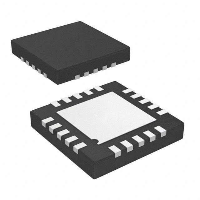
| 描述 | IC USB PORT PROTECTION 10SONESD 抑制器 Complete USB Port Prot Device |
| 产品分类 | |
| 品牌 | Texas Instruments |
| 产品手册 | http://www.ti.com/lit/gpn/tpd4s014 |
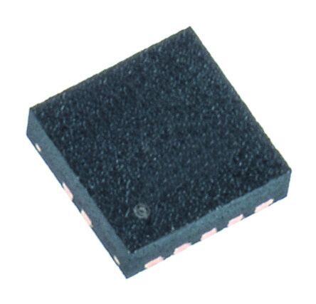
| 产品图片 |
|
| rohs | 符合RoHS无铅 / 符合限制有害物质指令(RoHS)规范要求 |
| 产品系列 | Texas Instruments TPD4S014DSQR- |
| 数据手册 | |
| 产品型号 | TPD4S014DSQR |
| PCN设计/规格 | |
| 产品种类 | ESD 抑制器 |
| 供应商器件封装 | 10-SON(2x2) |
| 其它名称 | 296-29093-6 |
| 击穿电压 | 6 V |
| 包装 | Digi-Reel® |
| 商标 | Texas Instruments |
| 安装类型 | 表面贴装 |
| 封装 | Reel |
| 封装/外壳 | 10-WFDFN 裸露焊盘 |
| 封装/箱体 | WSON-10 |
| 工厂包装数量 | 3000 |
| 应用 | 手机、媒体播放器 |
| 标准包装 | 1 |
| 电容 | 1.6 pF |
| 端接类型 | SMD/SMT |
| 类型 | 过压保护控制器 |
| 系列 | TPD4S014 |


- 商务部:美国ITC正式对集成电路等产品启动337调查
- 曝三星4nm工艺存在良率问题 高通将骁龙8 Gen1或转产台积电
- 太阳诱电将投资9.5亿元在常州建新厂生产MLCC 预计2023年完工
- 英特尔发布欧洲新工厂建设计划 深化IDM 2.0 战略
- 台积电先进制程称霸业界 有大客户加持明年业绩稳了
- 达到5530亿美元!SIA预计今年全球半导体销售额将创下新高
- 英特尔拟将自动驾驶子公司Mobileye上市 估值或超500亿美元
- 三星加码芯片和SET,合并消费电子和移动部门,撤换高东真等 CEO
- 三星电子宣布重大人事变动 还合并消费电子和移动部门
- 海关总署:前11个月进口集成电路产品价值2.52万亿元 增长14.8%


PDF Datasheet 数据手册内容提取
Product Sample & Technical Tools & Support & Folder Buy Documents Software Community TPD4S014 SLVSAU0G–MAY2011–REVISEDDECEMBER2015 TPD4S014 USB Charger Port Protection Including ESD Protection for All Lines and Overvoltage Protection on V BUS 1 Features 3 Description • InputVoltageProtectionatV upto28V The TPD4S014 is a single-chip solution for USB 1 BUS charger port protection. This device offers low • LowRonnFETSwitch capacitance transient voltage suppressor (TVS) • Supports>2AChargingCurrent electrostatic discharge (ESD) clamps for the D+, D–, • ESDPerformanceD+/D–/ID/VBUSPins: and standard capacitance for the ID pin. On the VBUS pin,thisdeviceprovidesovervoltageprotection(OVP) – ±15-kVContactDischarge(IEC61000-4-2) up to 28 V DC. The overvoltage lockout feature – ±15-kVAirGapDischarge(IEC61000-4-2) ensures that if there is a fault condition at the V BUS • OvervoltageandUndervoltageLockoutFeatures line, the TPD4S014 is able to isolate the V line to BUS protect the internal circuitry from damage. There is a • LowCapacitanceTVSESDClampforUSB2.0 17-ms turn-on delay after V rises above the HighSpeedDataRate BUS undervoltage lockout (UVLO) threshold in order to let • Internal17msStartupDelay the voltage stabilize before turning the nFET on. This • IntegratedInputEnableandStatusOutputSignal functionactsasade-glitchandpreventsunnecessary switching if there is any ringing on the line during • ThermalShutdownFeature connection. • SpaceSavingSONPackage(2mm×2mm) DeviceInformation(1) 2 Applications PARTNUMBER PACKAGE BODYSIZE(NOM) • CellPhones TPD4S014 WSON(10) 2.00mmx2.00mm • eBook (1) For all available packages, see the orderable addendum at • PortableMediaPlayers theendofthedatasheet. • DigitalCamera SimplifiedBlockDiagram V LOGIC 10 KΩ TPD4S014 ACK To Processor From Processor EN Battery V Charger BUS V OUT BUS 10 µF D- D+ ID 10 µF V BUS ort D- USB P B D+ Transceiver S U ID 1 An IMPORTANT NOTICE at the end of this data sheet addresses availability, warranty, changes, use in safety-critical applications, intellectualpropertymattersandotherimportantdisclaimers.PRODUCTIONDATA.
TPD4S014 SLVSAU0G–MAY2011–REVISEDDECEMBER2015 www.ti.com Table of Contents 1 Features.................................................................. 1 7.2 FunctionalBlockDiagram.......................................10 2 Applications........................................................... 1 7.3 FeatureDescription.................................................10 3 Description............................................................. 1 7.4 DeviceFunctionalModes........................................12 4 RevisionHistory..................................................... 2 8 ApplicationandImplementation........................ 13 8.1 ApplicationInformation............................................13 5 PinConfigurationandFunctions......................... 4 8.2 TypicalApplications................................................13 6 Specifications......................................................... 5 9 PowerSupplyRecommendations...................... 16 6.1 AbsoluteMaximumRatings......................................5 10 Layout................................................................... 16 6.2 ESDRatings..............................................................5 6.3 RecommendedOperatingConditions.......................5 10.1 LayoutGuidelines.................................................16 6.4 ThermalInformation..................................................6 10.2 LayoutExample....................................................17 6.5 ElectricalCharacteristics,EN,ACK,D+,D–,IDPins 11 DeviceandDocumentationSupport................. 18 ................................................................................... 6 11.1 CommunityResources..........................................18 6.6 ElectricalCharacteristicsOVPCircuits.....................7 11.2 Trademarks...........................................................18 6.7 SupplyCurrentConsumption....................................7 11.3 ElectrostaticDischargeCaution............................18 6.8 ThermalShutdownFeature......................................7 11.4 Glossary................................................................18 6.9 TypicalCharacteristics..............................................8 12 Mechanical,Packaging,andOrderable 7 DetailedDescription............................................ 10 Information........................................................... 18 7.1 Overview.................................................................10 4 Revision History NOTE:Pagenumbersforpreviousrevisionsmaydifferfrompagenumbersinthecurrentversion. ChangesfromRevisionF(September2015)toRevisionG Page • AddedafrequencytestconditiontocapacitanceintheElectricalCharacteristicstable. ..................................................... 6 ChangesfromRevisionE(June2014)toRevisionF Page • CorrectedV onnFETunderload................................................................................................................................... 10 DROP ChangesfromRevisionD(April2014)toRevisionE Page • UpdatedRecommendedOperatingConditionstable. ........................................................................................................... 5 • ChangedterminalnametoI fromI ................................................................................................................................. 6 LEAK L • UpdatedElectricalCharacteristicsOVPCircuitstable........................................................................................................... 7 • Changedt MAXvaluefrom18msto22ms ....................................................................................................................... 7 ON • Changedt 8µsvaluefromMAXtoTYP............................................................................................................................ 7 OFF • Changedt 11µsvaluefromMAXtoTYP...................................................................................................................... 7 d(OVP) • Changedt MAXvaluefrom9msto10.5ms. .................................................................................................................. 7 REC • UpdatedApplicationandImplementationsection. .............................................................................................................. 13 ChangesfromRevisionC(December2011)toRevisionD Page • AddedESDRatingstable....................................................................................................................................................... 5 • AddedRecommendedOperatingConditionstable................................................................................................................ 5 • AddedThermalInformationtable. ......................................................................................................................................... 6 • UpdatedElectricalCharacteristicsOVPCircuitstable........................................................................................................... 7 2 SubmitDocumentationFeedback Copyright©2011–2015,TexasInstrumentsIncorporated ProductFolderLinks:TPD4S014
TPD4S014 www.ti.com SLVSAU0G–MAY2011–REVISEDDECEMBER2015 ChangesfromRevisionB(October2011)toRevisionC Page • Madechangestothedatasheettotightentheparameters,VOP+changedfrom5.55Vto5.9V........................................ 1 • UpdatedDescription............................................................................................................................................................... 1 ChangesfromRevisionA(June2011)toRevisionB Page • ChangednameofV toV OUTthroughouttheentiredocument................................................................................... 10 CC BUS • DeletedrowfromDeviceOperationtable............................................................................................................................ 12 • AddedEyeDiagramstoTypicalCharacteristicssection...................................................................................................... 14 Copyright©2011–2015,TexasInstrumentsIncorporated SubmitDocumentationFeedback 3 ProductFolderLinks:TPD4S014
TPD4S014 SLVSAU0G–MAY2011–REVISEDDECEMBER2015 www.ti.com 5 Pin Configuration and Functions DSQPackage 10-PinWSON TopSide/See-ThroughView VBUSOUT 1 10 VBUS V OUT V BUS BUS EN GND ACK D+ ID 5 6 D- PinFunctions PIN TYPE DESCRIPTION NAME NO. VBUSOUT 1,2 PowerOutput ConnecttoPCBinternalPCBplane EN 3 IO EnableActive-LowInput.DriveENlowtoenabletheswitch.DriveENhightodisabletheswitch. Open-DrainAdapter-VoltageIndicatorOutput.ACKisdrivenlowaftertheVINvoltageisstable ACK 4 I betweenUVLOandOVLOfor17ms(typ).ConnectapullupresistorfromACKtothelogicI/O voltageofthehostsystem. ID 5 IO ESD-protectedline D– 6 IO ESD-protectedline D+ 7 IO ESD-protectedline GND 8 Ground Ground VBUS 9,10 USBInputPower ConnectorSideofVBUS CentralPAD CentralPAD HeatSink Electricallydisconnected.Useasheatsink.ConnecttoGNDplanevialargePCBPAD 4 SubmitDocumentationFeedback Copyright©2011–2015,TexasInstrumentsIncorporated ProductFolderLinks:TPD4S014
TPD4S014 www.ti.com SLVSAU0G–MAY2011–REVISEDDECEMBER2015 6 Specifications 6.1 Absolute Maximum Ratings overoperatingfree-airtemperaturerange(unlessotherwisenoted)(1)(2) MIN MAX UNIT Maximumjunctiontemperature –40 150 °C MaxVoltageonV –0.5 30 V BUS ContinuouscurrentthroughnFET 2.6 A ContinuouscurrentthroughACK –50 50 mA MaxCurrentthroughD+,D–,ID,V ESDclamps 50 mA BUS MaxvoltageonEN,ACK,D+,D-,ID,V OUT 6 V BUS Storagetemperature,T –65 150 °C stg (1) Stressesabovetheseratingsmaycausepermanentdamage.Exposuretoabsolutemaximumconditionsforextendedperiodsmay degradedevicereliability.Thesearestressratingsonly,andfunctionaloperationofthedeviceattheseoranyotherconditionsbeyond thosespecifiedisnotimplied. (2) Thealgebraicconvention,wherebythemostnegativevalueisaminimumandthemostpositivevalueisamaximum. 6.2 ESD Ratings VALUE UNIT Human-bodymodel(HBM),perANSI/ESDA/JEDECJS-001(1) ±2000 Charged-devicemodel(CDM),perJEDECspecificationJESD22-C101(2) ±1000 V Electrostaticdischarge V (ESD) IEC61000-4-2ContactDischarge D+,D–,ID,V pins ±1500 BUS IEC61000-4-2Air-gapDischarge D+,D–,ID,V pins ±1500 BUS (1) JEDECdocumentJEP155statesthat500-VHBMallowssafemanufacturingwithastandardESDcontrolprocess.Manufacturingwith lessthan500-VHBMispossiblewiththenecessaryprecautions.Pinslistedas±2000Vmayactuallyhavehigherperformance. (2) JEDECdocumentJEP157statesthat250-VCDMallowssafemanufacturingwithastandardESDcontrolprocess.Manufacturingwith lessthan250-VCDMispossiblewiththenecessaryprecautions.Pinslistedas±1000Vmayactuallyhavehigherperformance. 6.3 Recommended Operating Conditions overoperatingfree-airtemperaturerange(unlessotherwisenoted) MIN NOM MAX UNIT T Operatingfree-airtemperature –40 85 °C A V –0.1 5.5 BUSOUT V –0.1 5.5 BUS V Inputvoltage EN –0.1 5.5 V I ACK –0.1 5.5 D+,D-,ID, –0.1 5.5 I V continuouscurrent(1) V OUT 2.0 A VBUS BUS BUS C CapacitanceonV V Pin 10 µF VBUS BUS BUS C OUT CapacitanceonV OUT V OUTPin 10 µF VBUS BUS BUS R PullupresistoronACK ACKPin 10 kΩ ACK (1) IV Maxvalueisdependentonambienttemperature.SeeThermalShutdownsection. BUS Copyright©2011–2015,TexasInstrumentsIncorporated SubmitDocumentationFeedback 5 ProductFolderLinks:TPD4S014
TPD4S014 SLVSAU0G–MAY2011–REVISEDDECEMBER2015 www.ti.com 6.4 Thermal Information TPD4S014 THERMALMETRIC(1) DSQ(WSON) UNIT 8PINS R Junction-to-ambientthermalresistance 70.3 °C/W θJA R Junction-to-case(top)thermalresistance 46.3 °C/W θJCtop R Junction-to-boardthermalresistance 33.8 °C/W θJB ψ Junction-to-topcharacterizationparameter 2.9 °C/W JT ψ Junction-to-boardcharacterizationparameter 33.5 °C/W JB R Junction-to-case(bottom)thermalresistance 16.3 °C/W θJCbot (1) Formoreinformationabouttraditionalandnewthermalmetrics,seetheICPackageThermalMetricsapplicationreport,SPRA953. 6.5 Electrical Characteristics, EN, ACK, D+, D–, ID Pins overoperatingfree-airtemperaturerange(unlessotherwisenoted) PARAMETER TESTCONDITIONS MIN TYP MAX UNIT V High-levelinputvoltageEN Loadcurrent=50µA 1 V IH V Low-levelinputvoltageEN Loadcurrent=50µA 0.5 V IL I InputLeakageCurrentEN,D+,D–,ID V =3.3V 1 µA LEAK IO V Low-leveloutputvoltageACK I =2mA 0.1 V OL OL V DiodeforwardVoltageD+,D–,IDpins;lowerclampdiode I =8mA 0.95 V D O ΔC DifferentialCapacitancebetweentheD+,D–lines 0.03 pF IO C CapacitancetoGNDfortheD+,D–lines ƒ=1MHz 1.6 pF IO C CapacitancetoGNDfortheIDline 19 pF IO-ID V Reversestand-offvoltageofD+,D-andIDpins 5 V R V BreakdownvoltageD+,D–,IDpins I =1mA 6 V BR BR V BreakdownvoltageonV I =1mA 28 V BRVBUS BUS BR R DynamiconresistanceD+,D–,IDclamps I =1A 1 Ω DYN I 6 SubmitDocumentationFeedback Copyright©2011–2015,TexasInstrumentsIncorporated ProductFolderLinks:TPD4S014
TPD4S014 www.ti.com SLVSAU0G–MAY2011–REVISEDDECEMBER2015 6.6 Electrical Characteristics OVP Circuits overoperatingfree-airtemperaturerange(unlessotherwisenoted) PARAMETER TESTCONDITIONS MIN TYP MAX UNIT INPUTUNDERVOLTAGELOCKOUT VUVLO+ Udentdeecrte-vdoltthargeeshloocldk-roisuitn,ginputpower VpiBnUSincreasingfrom0Vto5V,NoloadonOUT 2.65 2.8 3 V VUVLO– Udentdeecrte-vdoltthargeeshloocldk-foaulltin,ginputpower VpiBnUSdecreasingfrom5Vto0V,NoloadonOUT 2.25 2.44 2.7 V VHYS-UVLO HysteresisonUVLO ΔofVUVLO+andVUVLO– 150 360 550 mV INPUTTOOUTPUTCHARACTERISTICS RDS_VBUSSWITCH VBUSswitchresistance VBUS=5V,IOUT=500mA 151 200 mΩ tON Turn-ONtime VRBLU=S3in6cΩre,aCsiLng=f1ro0muF2.8Vto4.75V,EN=0V, 16 17.4 22 ms tOFF Turn-OFFtime VRBLU=S3d6ecΩre,aCsLin=g1f0roumF2.44Vto0.5V,EN=0V, 8 µs INPUTOVERVOLTAGEPROTECTION(OVP) Inputover–voltage VOVP+ protectionthresholdrising VBUS VBUSincreasingfrom5Vto7V,NoLoad 5.9 6.15 6.45 V Inputover–voltage VOVP- protectionthresholdfalling VBUS VBUSdecreasingfrom7Vto5V,NoLoad 5.75 5.98 6.24 V VHYS-OVP HysteresisonOVP VBUS ΔofVOVP+andVOVP– 25 100 275 mV td(OVP) Overvoltagedelay VBUS RtoL7=V36Ω,CL=10µF;VBUSincreasingfrom5V 11 µs tREC Roveecrovvoelrtyagtiemceofnrodmitioinnput VBUS RtoL5=V36Ω,CL=10µF;VBUSdecreasingfrom7V 8 10.5 ms 6.7 Supply Current Consumption overoperatingfree-airtemperaturerange(unlessotherwisenoted) PARAMETER TESTCONDITIONS MIN TYP MAX UNIT I V OperatingCurrent NoloadonV pin,V =5V, 147.6 160 µA VBUS BUS BUS_OUT BUS Consumption EN=0V I V OperatingCurrent NoloadonV pin,V =5V, 111.8 120 µA VBUS_OFF BUS BUS_OUT BUS Consumption EN=5V 6.8 Thermal Shutdown Feature overoperatingfree-airtemperaturerange(unlessotherwisenoted) PARAMETER TESTCONDITIONS MIN TYP MAX UNIT T ThermalShutdown 144 °C SHDN T Thermal-ShutdownHysteresis 23 °C SHDN-HYS Copyright©2011–2015,TexasInstrumentsIncorporated SubmitDocumentationFeedback 7 ProductFolderLinks:TPD4S014
TPD4S014 SLVSAU0G–MAY2011–REVISEDDECEMBER2015 www.ti.com 6.9 Typical Characteristics Figure1.IEC61000-4-2-8-kVContactWaveform Figure2.IEC61000-4-2+8-kVContactWaveform Figure3.CapacitanceVariationWithVoltage Figure4.VariationofOnResistancewithAmbient Temperature Figure5.MaxPulseCurrentThroughSwitchvsPulse Figure6.UVLOThresholdVariationWithTemperature Duration 8 SubmitDocumentationFeedback Copyright©2011–2015,TexasInstrumentsIncorporated ProductFolderLinks:TPD4S014
TPD4S014 www.ti.com SLVSAU0G–MAY2011–REVISEDDECEMBER2015 Typical Characteristics (continued) Figure7.OVPThresholdVariationWithTemperature Figure8.StartUpInrushCurrentCharacteristics . Figure9.DeviceTurnonCharacteristics Figure10.DeviceTurnOFFCharacteristics(Undervoltage) Figure11.DeviceTurnOFFCharacteristics(Overvoltage) Copyright©2011–2015,TexasInstrumentsIncorporated SubmitDocumentationFeedback 9 ProductFolderLinks:TPD4S014
TPD4S014 SLVSAU0G–MAY2011–REVISEDDECEMBER2015 www.ti.com 7 Detailed Description 7.1 Overview The TPD4S014 provides a single-chip protection solution for USB charger interfaces. The V line is tolerant up BUS to 28 V DC. A Low RON nFET switch is used to disconnect the downstream circuits in case of a fault condition. At power-up, when the voltage on V is rising, the switch will close 17 ms after the input crosses the under BUS voltage threshold, thereby making power available to the downstream circuits. The TPD4S014 also has an ACK output, which de-asserts to alert the system a fault has occurred. The TPD4S014 offers 4 channel ESD clamps for D+, D-, ID, and V pins that provide IEC61000-4-2 level 4 ESD protection. This eliminates the need for BUS externalTVSclampcircuitsintheapplication. 7.2 Functional Block Diagram V V OUT BUS BUS Control Logic ACK + Internal OVLO Charge Pump Band Gap Reference UVLO EN GND D+ D- ID 7.3 Feature Description 7.3.1 InputVoltageProtectionatV upto28VDC BUS When the input voltage rises above V , or drops below the V , the internal V switch is turned off, OVP UVLO BUS removing power to the application. The ACK signal is de-asserted when a fault condition is detected. If the fault was an over voltage event, the V nFET switch turns on 8 ms (t ) after the input voltage returns below BUS REC V – V and remains above V If the fault was an under voltage event, the switch turns on 17 ms OVP HYS_OVP UVLO. after the voltage returns above V (similar to start up). When the switch turns on, the ACK is asserted once UVLO+ again. 7.3.2 LowRONnFETSwitch The nFET switch has a total on resistance (R ) of 151 mΩ. This equates to a voltage drop of 302 mV when ON charging at the maximum 2.0 A current level. Such low RON helps provide maximum potential to the system as providedbyanexternalcharger. 7.3.3 ESDPerformanceD+/D–/ID/V Pins BUS The D+, D–, ID, and V pins can withstand ESD events up to ±15-kV contact and air-gap. An ESD clamp BUS divertsthecurrenttoground. 10 SubmitDocumentationFeedback Copyright©2011–2015,TexasInstrumentsIncorporated ProductFolderLinks:TPD4S014
TPD4S014 www.ti.com SLVSAU0G–MAY2011–REVISEDDECEMBER2015 Feature Description (continued) 7.3.4 OvervoltageandUndervoltageLockoutFeatures The over voltage and under voltage lockout feature ensures that if there is a fault condition at the V line, the BUS TPD4S014 is able to isolate the V line and protect the internal circuitry from damage. Due to the body diode BUS ofthenFETswitch,ifthereisashorttogroundonV thesystemisexpectedtolimitthecurrenttoV OUT. BUS BUS 7.3.5 CapacitanceTVSESDClampforUSB2.0Hi-SpeedDataRate The D+/D– ESD protection pins have low capacitance so there is no significant impact to the signal integrity of theUSB2.0Hi-Speeddatarate. 7.3.6 Start-upDelay Upon startup, TPD4S014 has a built in startup delay. An internal oscillator controls a charge pump to control the turn-on delay (t ) of the internal nFET switch. The internal oscillator controls the timers that enable the turn-on ON of the charge pump and sets the state of the open-drain ACK output. If V < V or if V > V , the BUS UVLO BUS OVLO internal oscillator remains off, thus disabling the charge pump. At any time, if V drops below V or rises BUS UVLO aboveV ,ACKisreleasedandthenFETswitchisdisabled. OVLO 7.3.7 OVPGlitchImmunity A 17 ms deglitch time has been introduced into the turn on sequence to ensure that the input supply has stabilized before turning the nFET switch ON. Noise on the V line could turn ON the nFET switch when the BUS fault condition is still active. To avoid this, OVP glitch immunity allows noise on the V line to be rejected. Such BUS a glitch protection circuitry is also introduced in the turn off sequence in order to prevent the switch from turning off for voltage transients. The glitch protection circuitry integrates the glitch over time, allowing the OVP circuitry totriggerfasterforlargervoltageexcursionsabovetheOVPthresholdandslowerforshorterexcursions. 7.3.8 IntegratedInputEnableandStatusOutputSignal External control of the nFET switch is provided by an active low EN pin. An ACK pin provides output logic to acknowledgeV isbetweenUVLOandOVPbyassertinglow. BUS 7.3.9 ThermalShutdown When the device is ON, current flowing through the device will cause the device to heat up. Overheating can leadtopermanentdamagetothedevice.Topreventthis,anovertemperatureprotectionhasbeendesignedinto the device. Whenever the junction temperature exceeds 145ºC, the switch will turn off, thereby limiting the temperature. The ACK signal will be asserted for an over temperature event. Once the device cools down to below 120ºC the ACK signal will be de-asserted, and the switch will turn on if the EN is active and the V BUS voltage is within the UVLO and OVP thresholds. While the over temperature protection in the device will not kick- in unless the die temperature reaches 145ºC, it is generally recommended that care is taken to keep the junction temperature below 125 ºC. Operation of the device above 125 ºC for extended periods of time can affect the long-termreliabilityofthepart. Thejunctiontemperatureofthedevicecanbecalculatedusingbelowformula: T =T +P q j a D JA where • T =Junctiontemperature J • T =Ambienttemperature a • θ =Thermalresistance JA • P =Powerdissipatedindevice (1) D P =I2R D on where • I=Currentthroughdevice • R =Maxonresistanceofdevice (2) ON Copyright©2011–2015,TexasInstrumentsIncorporated SubmitDocumentationFeedback 11 ProductFolderLinks:TPD4S014
TPD4S014 SLVSAU0G–MAY2011–REVISEDDECEMBER2015 www.ti.com Feature Description (continued) Example At2-Acontinuouscurrentpowerdissipationisgivenby: P =22´0.2=0.8W D Iftheambienttemperatureisabout60°Cthejunctiontemperaturewillbe: T =60+(0.8´70.3)=116.24 j This implies that, at an ambient temperature of 60ºC, TPD4S014 can pass a continuous 2 A without sustaining damage. Conversely, the above calculation can also be used to calculate the total continuous current the TPD4S014canhandleatanygiventemperature. 7.4 Device Functional Modes Table1isthefunctiontableforTPD4S014. Table1.FunctionTable OTP UVLO OVLO EN SW ACK X H X X OFF H X X H X OFF H L L L H OFF L L L L L ON L H X X X OFF H OTP= Overtemperatureprotectioncircuitactive UVLO= Undervoltagelock-outcircuitactive OVLO= Overvoltagelock-outcircuitactive SW= Loadswitch CP= Chargepump X= Don’tCare H= True L= False 12 SubmitDocumentationFeedback Copyright©2011–2015,TexasInstrumentsIncorporated ProductFolderLinks:TPD4S014
TPD4S014 www.ti.com SLVSAU0G–MAY2011–REVISEDDECEMBER2015 8 Application and Implementation NOTE Information in the following applications sections is not part of the TI component specification, and TI does not warrant its accuracy or completeness. TI’s customers are responsible for determining suitability of components for their purposes. Customers should validateandtesttheirdesignimplementationtoconfirmsystemfunctionality. 8.1 Application Information The TPD4S014 is a single-chip solution for USB charger port protection. This device offers low capacitance TVS type ESD clamps for the D+, D–, and standard capacitance for the ID pin. On the V pin, this device can BUS handle over voltage protection up to 28 V. The over voltage lockout feature ensures that if there is a fault condition at the V line TPD4S014 is able to isolate the V line and protect the internal circuitry from BUS BUS damage. In order to let the voltage stabilize before closing the switch there is a 17 ms turn on delay after V BUS crosses the UVLO threshold. This function acts as a de-glitch which prevents unnecessary switching if there is any ringing on the line during connection. Due to the body diode of the nFET switch, if there is a short to ground onV thesystemisexpectedtolimitthecurrenttoV OUT. BUS BUS 8.2 Typical Applications 8.2.1 ForNon-OTGUSBSystems V LOGIC 10 KΩ TPD4S014 ACK To Processor From Processor EN Battery V Charger BUS V OUT BUS 10 µF D- D+ ID 10 µF V BUS ort D- USB P B D+ Transceiver S U ID Figure12. Non-OTGSchematic 8.2.1.1 DesignRequirements Table2showsthedesignparameters. Table2.DesignParameters DESIGNPARAMETERS EXAMPLEVALUE SignalrangeonV 3.3V–5.9V BUS SignalrangeonV OUT 3.9V–5.9V BUS SignalrangeonD+/D–andID 0V–5V DriveENlow(enabled) 0V–0.5V DriveENhigh(disabled) 1V–6V Copyright©2011–2015,TexasInstrumentsIncorporated SubmitDocumentationFeedback 13 ProductFolderLinks:TPD4S014
TPD4S014 SLVSAU0G–MAY2011–REVISEDDECEMBER2015 www.ti.com 8.2.1.2 DetailedDesignProcedure To begin the design process, some parameters must be decided upon. The designer needs to know the following: • V voltagerange BUS • ProcessorlogiclevelsV ,V forENandV ,V forACKpins OH OL IH IL 8.2.1.3 ApplicationCurves Figure13.EyeDiagramWithNoEVMandNoIC,Full Figure14.EyeDiagramWithEVM,NoIC,FullUSB2.0 USB2.0Speedat480Mbps Speedat480Mbps Figure15.EyeDiagramWithEVMandIC,FullUSB2.0Speedat480Mbps 14 SubmitDocumentationFeedback Copyright©2011–2015,TexasInstrumentsIncorporated ProductFolderLinks:TPD4S014
TPD4S014 www.ti.com SLVSAU0G–MAY2011–REVISEDDECEMBER2015 8.2.2 ForOTGUSBSystems V LOGIC To OTG power Current supply (5 V) 10 KΩ Limit Switch TPD4S014 ACK To Processor From Processor EN Battery V Charger BUS V OUT BUS 10 µF D- D+ ID 10 µF V BUS ort D- USB P B D+ Transceiver S U ID Figure16. OTGSchematic 8.2.2.1 DesignRequirements Table3showsthedesignparameters. Table3.DesignParameters DESIGNPARAMETERS EXAMPLEVALUE SignalrangeonV 3.3V–5.9V BUS SignalrangeonV OUT 3.9V–5.9V BUS SignalrangeonD+/D–andID 0V–5V DriveENlow(enabled) 0V–0.5V DriveENhigh(disabled) 1V–6V 8.2.2.2 DetailedDesignProcedure To begin the design process, some parameters must be decided upon. The designer needs to know the following: • V voltagerange BUS • ProcessorlogiclevelsV ,V forENandV ,V forACKpins OH OL IH IL • OTGpowersupplyoutputvoltagerange 8.2.2.3 ApplicationCurves RefertoApplicationCurvesintheprevioussection. Copyright©2011–2015,TexasInstrumentsIncorporated SubmitDocumentationFeedback 15 ProductFolderLinks:TPD4S014
TPD4S014 SLVSAU0G–MAY2011–REVISEDDECEMBER2015 www.ti.com 9 Power Supply Recommendations TPD4S014 Is designed to receive power from a USB 3.0 (or lower) V source. It can operate normally (nFET BUS ON) between 3.0 V and 5.9 V. Thus, the power supply (with a ripple of V ) requirement for TPD4S014 to be RIPPLE abletoswitchthenFETONisbetween3.0V+V and5.9V– V . RIPPLE RIPPLE 10 Layout 10.1 Layout Guidelines • Theoptimumplacementisasclosetotheconnectoraspossible. – EMI during an ESD event can couple from the trace being struck to other nearby unprotected traces, resultinginearlysystemfailures. – The PCB designer needs to minimize the possibility of EMI coupling by keeping any unprotected traces awayfromtheprotectedtraceswhicharebetweentheTVSandtheconnector. – KeeptracesbetweentheconnectorandTPD4S014onthesamelayerasTPD4S014. • Routetheprotectedtracesasstraightaspossible. • Eliminate any sharp corners on the protected traces between the TVS and the connector by using rounded cornerswiththelargestradiipossible. – Electricfieldstendtobuilduponcorners,increasingEMIcoupling. When designing layout for TPD4S014, note that V OUT and V pins allow for extra wide traces for good BUS BUS power delivery. In the example shown, these pins are routed with 25 mil (0.64 mm) wide traces. Place the V OUT and V capacitors as close to the device pins as possible. Pull ACK up to the Processor logic level BUS BUS high with a resistor. Use external and internal ground planes and stitch them together with VIAs as close to the GND pins of TPD4S014 as possible. This allows for a low impedance path to ground so that the device can properlydissipateanyESDevents. 16 SubmitDocumentationFeedback Copyright©2011–2015,TexasInstrumentsIncorporated ProductFolderLinks:TPD4S014
TPD4S014 www.ti.com SLVSAU0G–MAY2011–REVISEDDECEMBER2015 10.2 Layout Example Legend VIAto Power Ground Plane Processor Signal VIA V LOGIC Trace on alternate layer ACK EN V PoweLrO GGICround 10 KΩ USB SYS USB PORT 1 V V OUT V BUS BUS V BUS BUS D- D+ D- ID D+ ID Figure17. LayoutRecommendation Copyright©2011–2015,TexasInstrumentsIncorporated SubmitDocumentationFeedback 17 ProductFolderLinks:TPD4S014
TPD4S014 SLVSAU0G–MAY2011–REVISEDDECEMBER2015 www.ti.com 11 Device and Documentation Support 11.1 Community Resources The following links connect to TI community resources. Linked contents are provided "AS IS" by the respective contributors. They do not constitute TI specifications and do not necessarily reflect TI's views; see TI's Terms of Use. TIE2E™OnlineCommunity TI'sEngineer-to-Engineer(E2E)Community.Createdtofostercollaboration amongengineers.Ate2e.ti.com,youcanaskquestions,shareknowledge,exploreideasandhelp solveproblemswithfellowengineers. DesignSupport TI'sDesignSupport QuicklyfindhelpfulE2Eforumsalongwithdesignsupporttoolsand contactinformationfortechnicalsupport. 11.2 Trademarks E2EisatrademarkofTexasInstruments. Allothertrademarksarethepropertyoftheirrespectiveowners. 11.3 Electrostatic Discharge Caution Thesedeviceshavelimitedbuilt-inESDprotection.Theleadsshouldbeshortedtogetherorthedeviceplacedinconductivefoam duringstorageorhandlingtopreventelectrostaticdamagetotheMOSgates. 11.4 Glossary SLYZ022—TIGlossary. Thisglossarylistsandexplainsterms,acronyms,anddefinitions. 12 Mechanical, Packaging, and Orderable Information The following pages include mechanical, packaging, and orderable information. This information is the most current data available for the designated devices. This data is subject to change without notice and revision of thisdocument.Forbrowser-basedversionsofthisdatasheet,refertotheleft-handnavigation. 18 SubmitDocumentationFeedback Copyright©2011–2015,TexasInstrumentsIncorporated ProductFolderLinks:TPD4S014
PACKAGE OPTION ADDENDUM www.ti.com 6-Feb-2020 PACKAGING INFORMATION Orderable Device Status Package Type Package Pins Package Eco Plan Lead/Ball Finish MSL Peak Temp Op Temp (°C) Device Marking Samples (1) Drawing Qty (2) (6) (3) (4/5) TPD4S014DSQR ACTIVE WSON DSQ 10 3000 Green (RoHS NIPDAU Level-2-260C-1 YEAR -40 to 85 ZTE & no Sb/Br) (1) The marketing status values are defined as follows: ACTIVE: Product device recommended for new designs. LIFEBUY: TI has announced that the device will be discontinued, and a lifetime-buy period is in effect. NRND: Not recommended for new designs. Device is in production to support existing customers, but TI does not recommend using this part in a new design. PREVIEW: Device has been announced but is not in production. Samples may or may not be available. OBSOLETE: TI has discontinued the production of the device. (2) RoHS: TI defines "RoHS" to mean semiconductor products that are compliant with the current EU RoHS requirements for all 10 RoHS substances, including the requirement that RoHS substance do not exceed 0.1% by weight in homogeneous materials. Where designed to be soldered at high temperatures, "RoHS" products are suitable for use in specified lead-free processes. TI may reference these types of products as "Pb-Free". RoHS Exempt: TI defines "RoHS Exempt" to mean products that contain lead but are compliant with EU RoHS pursuant to a specific EU RoHS exemption. Green: TI defines "Green" to mean the content of Chlorine (Cl) and Bromine (Br) based flame retardants meet JS709B low halogen requirements of <=1000ppm threshold. Antimony trioxide based flame retardants must also meet the <=1000ppm threshold requirement. (3) MSL, Peak Temp. - The Moisture Sensitivity Level rating according to the JEDEC industry standard classifications, and peak solder temperature. (4) There may be additional marking, which relates to the logo, the lot trace code information, or the environmental category on the device. (5) Multiple Device Markings will be inside parentheses. Only one Device Marking contained in parentheses and separated by a "~" will appear on a device. If a line is indented then it is a continuation of the previous line and the two combined represent the entire Device Marking for that device. (6) Lead/Ball Finish - Orderable Devices may have multiple material finish options. Finish options are separated by a vertical ruled line. Lead/Ball Finish values may wrap to two lines if the finish value exceeds the maximum column width. Important Information and Disclaimer:The information provided on this page represents TI's knowledge and belief as of the date that it is provided. TI bases its knowledge and belief on information provided by third parties, and makes no representation or warranty as to the accuracy of such information. Efforts are underway to better integrate information from third parties. TI has taken and continues to take reasonable steps to provide representative and accurate information but may not have conducted destructive testing or chemical analysis on incoming materials and chemicals. TI and TI suppliers consider certain information to be proprietary, and thus CAS numbers and other limited information may not be available for release. In no event shall TI's liability arising out of such information exceed the total purchase price of the TI part(s) at issue in this document sold by TI to Customer on an annual basis. Addendum-Page 1
PACKAGE MATERIALS INFORMATION www.ti.com 3-Aug-2017 TAPE AND REEL INFORMATION *Alldimensionsarenominal Device Package Package Pins SPQ Reel Reel A0 B0 K0 P1 W Pin1 Type Drawing Diameter Width (mm) (mm) (mm) (mm) (mm) Quadrant (mm) W1(mm) TPD4S014DSQR WSON DSQ 10 3000 179.0 8.4 2.2 2.2 1.2 4.0 8.0 Q2 PackMaterials-Page1
PACKAGE MATERIALS INFORMATION www.ti.com 3-Aug-2017 *Alldimensionsarenominal Device PackageType PackageDrawing Pins SPQ Length(mm) Width(mm) Height(mm) TPD4S014DSQR WSON DSQ 10 3000 195.0 200.0 45.0 PackMaterials-Page2
PACKAGE OUTLINE DSQ0010A WSON - 0.8 mm max height SCALE 5.000 PLASTIC SMALL OUTLINE - NO LEAD 2.1 B A 1.9 PIN 1 INDEX AREA 2.1 1.9 0.8 C 0.7 SEATING PLANE 0.05 0.00 0.08 C 0.9 0.1 EXPOSED SYMM (0.2) TYP THERMAL PAD 5 6 SYMM 11 2X 1.6 1.5 0.1 8X 0.4 1 10 0.25 PIN 1 ID 10X 0.15 0.4 10X 0.2 0.1 C A B 0.05 4218906/A 04/2019 NOTES: 1. All linear dimensions are in millimeters. Any dimensions in parenthesis are for reference only. Dimensioning and tolerancing per ASME Y14.5M. 2. This drawing is subject to change without notice. 3. The package thermal pad must be soldered to the printed circuit board for thermal and mechanical performance. www.ti.com
EXAMPLE BOARD LAYOUT DSQ0010A WSON - 0.8 mm max height PLASTIC SMALL OUTLINE - NO LEAD (0.9) SEE SOLDER MASK 10X (0.5) DETAIL SYMM 10 10X (0.2) 1 (1.5) 8X (0.4) 11 SYMM (0.5) (R0.05) TYP 5 6 ( 0.2) TYP VIA (1.9) LAND PATTERN EXAMPLE EXPOSED METAL SHOWN SCALE: 20X 0.07 MIN 0.07 MAX ALL AROUND ALL AROUND METAL UNDER METAL EDGE SOLDER MASK EXPOSED METAL SOLDER MASK EXPOSED SOLDER MASK OPENING METAL OPENING NON SOLDER MASK DEFINED SOLDER MASK DEFINED (PREFERRED) SOLDER MASK DETAILS 4218906/A 04/2019 NOTES: (continued) 4. This package is designed to be soldered to a thermal pad on the board. For more information, see Texas Instruments literature number SLUA271 (www.ti.com/lit/slua271). 5. Vias are optional depending on application, refer to device data sheet. If any vias are implemented, refer to their locations shown on this view. It is recommended that vias under paste be filled, plugged or tented. www.ti.com
EXAMPLE STENCIL DESIGN DSQ0010A WSON - 0.8 mm max height PLASTIC SMALL OUTLINE - NO LEAD 10X (0.5) (0.85) 10X (0.2) 1 10 8X (0.4) 11 SYMM (1.38) (R0.05) TYP 5 6 SYMM (1.9) SOLDER PASTE EXAMPLE BASED ON 0.125 MM THICK STENCIL SCALE: 20X EXPOSED PAD 11 87% PRINTED SOLDER COVERAGE BY AREA UNDER PACKAGE 4218906/A 04/2019 NOTES: (continued) 6. Laser cutting apertures with trapezoidal walls and rounded corners may offer better paste release. IPC-7525 may have alternate design recommendations. www.ti.com
IMPORTANTNOTICEANDDISCLAIMER TI PROVIDES TECHNICAL AND RELIABILITY DATA (INCLUDING DATASHEETS), DESIGN RESOURCES (INCLUDING REFERENCE DESIGNS), APPLICATION OR OTHER DESIGN ADVICE, WEB TOOLS, SAFETY INFORMATION, AND OTHER RESOURCES “AS IS” AND WITH ALL FAULTS, AND DISCLAIMS ALL WARRANTIES, EXPRESS AND IMPLIED, INCLUDING WITHOUT LIMITATION ANY IMPLIED WARRANTIES OF MERCHANTABILITY, FITNESS FOR A PARTICULAR PURPOSE OR NON-INFRINGEMENT OF THIRD PARTY INTELLECTUAL PROPERTY RIGHTS. These resources are intended for skilled developers designing with TI products. You are solely responsible for (1) selecting the appropriate TI products for your application, (2) designing, validating and testing your application, and (3) ensuring your application meets applicable standards, and any other safety, security, or other requirements. These resources are subject to change without notice. TI grants you permission to use these resources only for development of an application that uses the TI products described in the resource. Other reproduction and display of these resources is prohibited. No license is granted to any other TI intellectual property right or to any third party intellectual property right. TI disclaims responsibility for, and you will fully indemnify TI and its representatives against, any claims, damages, costs, losses, and liabilities arising out of your use of these resources. TI’s products are provided subject to TI’s Terms of Sale (www.ti.com/legal/termsofsale.html) or other applicable terms available either on ti.com or provided in conjunction with such TI products. TI’s provision of these resources does not expand or otherwise alter TI’s applicable warranties or warranty disclaimers for TI products. Mailing Address: Texas Instruments, Post Office Box 655303, Dallas, Texas 75265 Copyright © 2020, Texas Instruments Incorporated