 Datasheet下载
- 型号: CM2020-00TR
- 制造商: ON Semiconductor
- 库位|库存: xxxx|xxxx
- 要求:
| 数量阶梯 | 香港交货 | 国内含税 |
| +xxxx | $xxxx | ¥xxxx |
查看当月历史价格
查看今年历史价格
CM2020-00TR产品简介:
ICGOO电子元器件商城为您提供CM2020-00TR由ON Semiconductor设计生产,在icgoo商城现货销售,并且可以通过原厂、代理商等渠道进行代购。 CM2020-00TR价格参考。ON SemiconductorCM2020-00TR封装/规格:专用 IC, HDMI Port Protection 38-TSSOP。您可以下载CM2020-00TR参考资料、Datasheet数据手册功能说明书,资料中有CM2020-00TR 详细功能的应用电路图电压和使用方法及教程。
CM2020-00TR是安森美(ON Semiconductor)推出的一款专用IC,主要用于USB充电端口的智能电源管理与充电协议识别。该芯片符合USB BC1.2(Battery Charging 1.2)标准,可自动检测连接设备的类型,支持多种充电模式,包括标准下行端口(SDP)、充电下行端口(CDP)和专用充电端口(DCP),从而优化充电电流并提升充电效率。

该器件广泛应用于消费类电子产品中需要为便携设备提供快速、安全充电的场景,如车载充电器、壁式充电器、移动电源(充电宝)、多端口桌面充电站以及带充电功能的智能家居设备等。CM2020-00TR通过集成高精度电流检测和电压调节功能,确保充电过程稳定可靠,并具备过压、过流和短路保护机制,有效提升系统安全性。

此外,该芯片采用小型化封装(如DFN),节省PCB空间,适合对体积要求较高的便携式设备设计。其低功耗特性和高集成度使其在无需微控制器干预的情况下实现自主运行,简化了系统设计,降低了整体成本。因此,CM2020-00TR是各类通用或专用充电设备中实现智能识别与高效充电的理想解决方案。
| 参数 | 数值 |
| 产品目录 | |
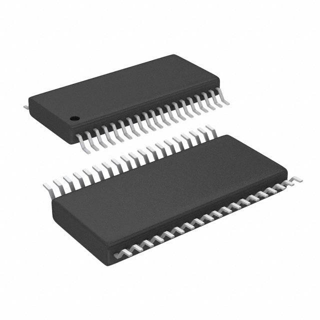
| 描述 | IC HDMI TX PORT P/I 38-TSSOPESD 抑制器 HDMI Port P/I Device Transmitter |
| 产品分类 | |
| 品牌 | ON Semiconductor |
| 产品手册 | |
| 产品图片 |
|
| rohs | 符合RoHS无铅 / 符合限制有害物质指令(RoHS)规范要求 |
| 产品系列 | ON Semiconductor CM2020-00TR- |
| 数据手册 | |
| 产品型号 | CM2020-00TR |
| 产品种类 | ESD 抑制器 |
| 供应商器件封装 | 38-TSSOP |
| 其它名称 | CM2020-00TROSDKR |
| 包装 | Digi-Reel® |
| 商标 | ON Semiconductor |
| 安装类型 | 表面贴装 |
| 封装 | Reel |
| 封装/外壳 | 38-TFSOP (0.173",4.40mm 宽)裸焊盘 |
| 封装/箱体 | TSSOP-38 |
| 工作温度范围 | - 40 C to + 85 C |
| 工作电压 | 6 V |
| 工厂包装数量 | 2500 |
| 应用 | 消费电子,DVD-RW 播放器,机顶盒 |
| 标准包装 | 1 |
| 电容 | 0.9 pF |
| 电流额定值 | 110 uA |
| 端接类型 | Solder Pad |
| 类型 | HDMI 发射器 |
| 系列 | CM2020-00TR |


- 商务部:美国ITC正式对集成电路等产品启动337调查
- 曝三星4nm工艺存在良率问题 高通将骁龙8 Gen1或转产台积电
- 太阳诱电将投资9.5亿元在常州建新厂生产MLCC 预计2023年完工
- 英特尔发布欧洲新工厂建设计划 深化IDM 2.0 战略
- 台积电先进制程称霸业界 有大客户加持明年业绩稳了
- 达到5530亿美元!SIA预计今年全球半导体销售额将创下新高
- 英特尔拟将自动驾驶子公司Mobileye上市 估值或超500亿美元
- 三星加码芯片和SET,合并消费电子和移动部门,撤换高东真等 CEO
- 三星电子宣布重大人事变动 还合并消费电子和移动部门
- 海关总署:前11个月进口集成电路产品价值2.52万亿元 增长14.8%


PDF Datasheet 数据手册内容提取
CM2020-00TR HDMI Transmitter Port Protection and Interface Device Product Description The CM2020−00TR HDMI Transmitter Port Protection and http://onsemi.com Interface device is specifically designed for next generation HDMI source interface protection. An integrated package provides all ESD, level shift, overcurrent output protection and backdrive protection for an HDMI port in asingle 38−Pin TSSOP package. The CM2020−00TR part is specifically designed to complement the CM2021 protection part in HDMI receivers (Displays, DTV, CEdevices, etc.) TSSOP 38 The CM2020−00TR also incorporates a silicon overcurrent TR SUFFIX CASE 948AG protection device for +5V supply voltage output to the connector. Features MARKING DIAGRAM • HDMI 1.3 Compliant • 0.05pF Matching Capacitance between the TMDS Intra−Pair • CM2020−00TR Overcurrent Output Protection • Level Shifting/Isolation Circuitry • CM2020−00TR = Specific Device Code Provides ESD Protection to IEC61000−4−2 Level 4 ♦ 8kV Contact Discharge ORDERING INFORMATION ♦ 15kV Air Discharge • Matched 0.5mm Trace Spacing (TSSOP) Device Package Shipping† • Simplified Layout for HDMI Connectors CM2020−00TR TSSOP−38 2500/Tape & Reel • (Pb−Free) Backdrive Protection • †For information on tape and reel specifications, These Devices are Pb−Free and are RoHS Compliant including part orientation and tape sizes, please refer to our Tape and Reel Packaging Specification Applications Brochure, BRD8011/D. • PC • Consumer Electronics • Set Top Box • DVDRW Players © Semiconductor Components Industries, LLC, 2011 1 Publication Order Number: April, 2011 − Rev. 5 CM2020−00TR/D
CM2020−00TR ELECTRICAL SCHEMATIC ESD_BYP 5V_SUPPLY TMDS_D2+ TMDS_D1+ TMDS_D0+ TMDS_CK+ TMDS_GND TMDS_GND TMDS_GND TMDS_GND TMDS_D2− TMDS_D1− TMDS_D0− TMDS_CK− LV SUPPLY LV SUPPLY CE_REMOTE_IN DDC_DAT_OUT CE_REMOTE_OUT DDC_DAT_IN LV SUPPLY LV SUPPLY DDC_CLK_IN HOTPLUG_DET_OUT DDC_CLK_OUT HOTPLUG_DET_IN 55 mA 5V_SUPPLY Overcurrent 5V_OUT Switch PACKAGE / PINOUT DIAGRAM Top View 5V_SUPPLY 1 38 5V_OUT LV_SUPPLY 2 37 ESD_BYP GND 3 36 GND TMDS_D2+ 4 35 TMDS_D2+ TMDS_GND 5 34 TMDS_GND TMDS_D2− 6 33 TMDS_D2− TMDS_D1+ 7 32 TMDS_D1+ TMDS_GND 8 31 TMDS_GND TMDS_D1− 9 30 TMDS_D1− TMDS_D0+ 10 29 TMDS_D0+ TMDS_GND 11 28 TMDS_GND TMDS_D0− 12 27 TMDS_D0− TMDS_CK+ 13 26 TMDS_CK+ TMDS_GND 14 25 TMDS_GND TMDS_CK− 15 24 TMDS_CK− CE_REMOTE_IN 16 23 CE_REMOTE_OUT DDC_CLK_IN 17 22 DDC_CLK_OUT DDC_DAT_IN 18 21 DDC_DAT_OUT HOTPLUG_DET_IN 19 20 HOTPLUG_DET_OUT 38−Pin TSSOP Package http://onsemi.com 2
CM2020−00TR Table 1. PIN DESCRIPTIONS Pins Name ESD Level Description 4, 35 TMDS_D2+ 8 kV (Note 3) TMDS 0.9 pF ESD Protection (Note 1) 6, 33 TMDS_D2− 8 kV (Note 3) TMDS 0.9 pF ESD Protection (Note 1) 7, 32 TMDS_D1+ 8 kV (Note 3) TMDS 0.9 pF ESD Protection (Note 1) 9, 30 TMDS_D1− 8 kV (Note 3) TMDS 0.9 pF ESD Protection (Note 1) 10, 29 TMDS_D0+ 8 kV (Note 3) TMDS 0.9 pF ESD Protection (Note 1) 12, 27 TMDS_D0− 8 kV (Note 3) TMDS 0.9 pF ESD Protection (Note 1) 13, 26 TMDS_CK+ 8 kV (Note 3) TMDS 0.9 pF ESD Protection (Note 1) 15, 24 TMDS_CK− 8 kV (Note 3) TMDS 0.9 pF ESD Protection (Note 1) 16 CE_REMOTE_IN 2 kV (Note 4) LV_SUPPLY Referenced Logic Level into ASIC 23 CE_REMOTE_OUT 8 kV(Note 3) 5V_SUPPLY Referenced Logic Level Out plus 3.5 pF ESD to Connector 17 DDC_CLK_IN 2 kV (Note 4) LV_SUPPLY Referenced Logic Level into ASIC 22 DDC_CLK_OUT 8 kV (Note 3) 5V_SUPPLY Referenced Logic Level Out plus 3.5 pF ESD to Connector 18 DDC_DAT_IN 2 kV (Note 4) LV_SUPPLY Referenced Logic Level into ASIC 21 DDC_DAT_OUT 8 kV (Note 3) 5V_SUPPLY Referenced Logic Level Out plus 3.5 pF ESD to Connector 19 HOTPLUG_DET_IN 2 kV (Note 4) LV_SUPPLY Referenced Logic Level into ASIC 20 HOTPLUG_DET_OUT 8 kV (Note 3) 5V_SUPPLY Referenced Logic Level Out plus 3.5 pF ESD (Note 2) to Connector 2 LV_SUPPLY 2 kV (Note 4) Bias for CE / DDC / HOTPLUG Level Shifters 1 5V_SUPPLY 2 kV (Note 4) Current Source for 5V_OUT 38 5V_OUT 8 kV (Note 3) 55 mA Minimum Overcurrent Protected 5 V Output. This Output Must be Bypassed with a 0.1 (cid:2)F Ceramic Capacitor. 37 ESD_BYP 2 kV (Note 4) This Pin must be Connected to a 0.1 (cid:2)F Ceramic Capacitor 3, 36 GND N/A Supply GND Reference 5, 34, 8, TMDS_GND N/A TMDS ESD and Parasitic GND Return (Note 5) 31, 11, 28, 14, 25 1. These 2 pins need to be connected together in−line on the PCB. 2. This output can be connected to an external 0.1 (cid:2)F ceramic capacitor, resulting in an increased ESD withstand voltage rating. 3. Standard IEC 61000−4−2, CDISCHARGE = 150 pF, RDISCHARGE = 330 (cid:3), 5V_SUPPLY and LV_SUPPLY within recommended operating conditions, GND = 0 V and ESD_BYP (pin 37), 5V_OUT (pin 38), and HOTPLUG_DET_OUT (pin 20) each bypassed with a 0.1 (cid:2)F ceramic capacitor connected to GND. 4. Human Body Model per MIL−STD−883, Method 3015, CDISCHARGE = 100 pF, RDISCHARGE = 1.5 k(cid:3), 5V_SUPPLY and LV_SUPPLY within recommended operating conditions, GND = 0 V and ESD_BYP (pin 37), 5V_OUT (pin 38), and HOTPLUG_DET_OUT (pin 20) each bypassed with a 0.1 (cid:2)F ceramic capacitor connected to GND. 5. These pins should be routed directly to the associated GND pins on the HDMI connector with single point ground vias at the connector. http://onsemi.com 3
CM2020−00TR BACKDRIVE PROTECTION Below, two scenarios are discussed to illustrate what can In a more serious scenario, if any SOC devices are happen when a powered device is connected to an incorporated in the design which have built−in level shifter unpowered device via a HDMI interface, substantiating the and DRC diodes for ESD protection, there is even a risk for need for backdrive protection on this type of interface. permanent damage. In this case, if there is a pullup resistor In the first example a DVD player is connected to a TV via (such as with DDC) on the other end of the cable, then that an HDMI interface. If the DVD player is switched off and resistance will pull the SOC chips “output” up to a high the TV is left on, there is a possibility of reverse current flow level. This will forward bias the upper ESD diode in the back into the main power supply rail of the DVD player. DRC and charge the bulk capacitance in a similar fashion as Typically, the DVD’s power supply has some form of bulk described in the first example. If this current flow is high supply capacitance associated with it. Because all CMOS enough, even as little as a few milliamps, it could destroy logic exhibits a very high impedance on the power rail node one of the SOC chip’s internal DRC diodes, as they are not when “off”, if there may be very little parasitic shunt designed for passing DC. resistance, and even with as little as a few milliamps of To avoid either of these situations, the CM2020−00TR “backdrive” current flowing into the power rail, it is possible was designed to block backdrive current, guaranteeing no over time to charge that bulk supply capacitance to some more than 5 mA on any I/O pin when the I/O pin voltage is intermediate level. If this level rises above the greater than the CM2020−00TR supply voltage. power−on−reset (POR) voltage level of some of the integrated circuits in the DVD player, these devices may not reset properly when the DVD player is turned back on. Figure 1. Backdrive Protection Diagram. SPECIFICATIONS Table 2. ABSOLUTE MAXIMUM RATINGS Parameter Rating Units VCC5V, VCCLV 6.0 V DC Voltage at any Channel Input 6.0 V Storage Temperature Range −65 to +150 °C Stresses exceeding Maximum Ratings may damage the device. Maximum Ratings are stress ratings only. Functional operation above the Recommended Operating Conditions is not implied. Extended exposure to stresses above the Recommended Operating Conditions may affect device reliability. Table 3. STANDARD (RECOMMENDED) OPERATING CONDITIONS Symbol Parameter Min Typ Max Units 5V_SUPPLY Operating Supply Voltage GND 5 5.5 V LV_SUPPLY Bias Supply Voltage 1 3.3 5.5 V − Operating Temperature Range –40 − 85 °C http://onsemi.com 4
CM2020−00TR SPECIFICATIONS (Cont’d) Table 4. ELECTRICAL OPERATING CHARACTERISTICS (Note 1) Symbol Parameter Conditions Min Typ Max Units ICC5V Operating Supply Current 5V_SUPPLY = 5.0 V 110 130 (cid:2)A ICCLV Bias Supply Current LV_SUPPLY = 3.3 V 1 5 (cid:2)A VDROP 5V_OUT Overcurrent Output Drop 5V_SUPPLY = 5.0 V, 65 100 mV IOUT = 55 mA ISC 5V_OUT Short Circuit Current Limit 5V_SUPPLY = 5.0 V, 90 135 175 mA 5V_OUT = GND IOFF OFF State Leakage Current, Level Shifting LV_SUPPLY = 0 V 0.1 5.0 (cid:2)A NFET IBACKDRIVE Current Conducted from Output Pins to 5V_SUPPLY < VCH_OUT 0.1 5.0 (cid:2)A V_SUPPLY Rails when Powered Down Signal Pins: TMDS_D[2:0]+/−, TMDS_CK+/−, CE_REMOTE_OUT, DDC_DAT_OUT, DDC_CLK_OUT, HOTPLUG_DET_OUT, 5V_OUT Only IBACKDRIVE, Current through CE−REMOTE_OUT when CE−REMOTE_IN = LV_SUPPLY < 0.1 1.0 (cid:2)A CEC Powered Down CE_REMOTE_OUT VON VOLTAGE Drop Across Level Shifting NFET LV_SUPPLY = 2.5 V, VS = GND, 75 95 140 mV when ON IDS = 3 mA VF Diode Forward Voltage IF = 8 mA, TA = 25°C V Top Diode 0.60 0.85 0.95 Bottom Diode 0.60 0.85 0.95 VESD ESD Withstand Voltage, Contact Discharge Pins 4, 7, 10, 13, 20, 21, 22, 23, 24, ±8 kV per IEC 61000−4−2 Standard (IEC) 27, 30, 33, 38; TA = 25°C (Note 2) VCL Channel Clamp Voltage TA = 25°C, IPP = 1 A, tP = 8/20 uS V Positive Transients (Note 3) 10.8 Negative Transients −2.1 RDYN Dynamic Resistance IPP = 1 A, tP = 8/20 (cid:2)S, TA = 25°C (cid:3) Positive Transients (Note 3) 1.4 Negative Transients 0.9 ILEAK TMDS Channel Leakage Current TA = 25°C 0.01 1 (cid:2)A CIN, TMDS TMDS Channel Input Capacitance 5V_SUPPLY = 5.0 V, Measured at 0.9 1.2 pF 1MHz, VBIAS = 2.5 V (cid:4)CIN, TMDS TMDS Channel Input Capacitance Matching 5V_SUPPLY = 5.0 V, Measured at 0.05 pF 1MHz, VBIAS = 2.5 V (Note 4) CIN, DDC Level Shifting Input Capacitance, Capacitance 5V_SUPPLY = 5.0 V, Measured at 3.5 4 pF to GND 100kHz, VBIAS = 2.5 V (Note 2) CIN, CEC Level Shifting Input Capacitance, Capacitance 5V_SUPPLY = 5.0 V, Measured at 3.5 4 pF to GND 100kHz, VBIAS = 2.5 V CIN, HP Level Shifting Input Capacitance, Capacitance 5V_SUPPLY = 5.0 V, Measured at 3.5 4 pF to GND 100kHz, VBIAS = 2.5 V 1. Operating Characteristics are over Standard Operating Conditions unless otherwise specified. 2. Standard IEC 61000−4−2, CDISCHARGE = 150 pF, RDISCHARGE = 330 (cid:3), 5V_SUPPLY and LV_SUPPLY within recommended operating conditions, GND = 0 V and ESD_BYP (pin 37), 5V_OUT (pin 38), and HOTPLUG_DET_OUT (pin 20) each bypassed with a 0.1 (cid:2)F ceramic capacitor connected to GND. 3. These measurements performed with no external capacitor on ESD_BYP. 4. Intra−pair matching, each TMDS pair (i.e. D+, D−). http://onsemi.com 5
CM2020−00TR PERFORMANCE INFORMATION Typical Filter Performance (TA = 25°C, DC Bias = 0 V, 50 (cid:2) Environment) Figure 2. Insertion Loss vs. Frequency (TMDS_D1− to GND) http://onsemi.com 6
CM2020−00TR APPLICATION INFORMATION LAYOUT NOTES NOTE 1) Differential TMDS Pairs should be designed as normal 100W HDMI microstrip. Single Ended TMDS traces underneath CM2020 and between CM2020 and Connector should be tuned to match chip/connector parasitics. (See MediaGuard] Application Notes.) NOTE 2) Level Shifter signals should be biased with a weak pullup to the desired local LV_SUPPLY. If the local ASIC includes sufficient pullups to register a logic high when the CM2020 NFET is “off”, then external pullups are not needed NOTE 3) Place CM2020 as close to conector as possible, and as with any controlled impedance line avoid ANY silkscreening over TMDS lines. NOTE 4) CEC pullup isolation. The 27k RCEC and a Schottky DCEC provide the necessary isolation for the CEC pullup. Figure 3. Typical Application for CM2020−00TR http://onsemi.com 7
CM2020−00TR APPLICATION INFORMATION (Cont’d) Design Considerations ESD Bypass Pin 37 (ESD_BYP) is provided for an optional external ESD bypass capacitor only (i.e. 0.1 (cid:2)F ceramic). It should not be connected to any supply rail. 5V Overcurrent Output Maximum Overcurrent Protection output drop at 55 mA on 5V_OUT is 100 mV. To meet HDMI output requirements of 4.8−5.3V, an input of greater than 4.9V should be used (i.e. 5.1V ±4%). A 0.1(cid:2)F ceramic bypass capacitor on this output is also recommended. Hotplug Detect Input To meet the requirements of HDMI CTS TID7−12, the following pullup/pulldown configuration is recommended for a3.3V ±10% internal VCC rail (See Figure 4 below). A 0.1 (cid:2)F ceramic capacitor is recommended for additional edge debounce and ESD bypass. DUT On vs. DUT Off Many HDMI CTS tests require a power off condition on the System Under Test. Many Dual Rail Clamp (DRC) ESD diode configurations will be forward biased when their VDD rail is lower than the I/O pin bias, thereby exhibiting extremely high apparent capacitance measurements, for example. The MediaGuard(cid:2) backdrive isolation circuitry limits this current to <5(cid:2)A, and will help ensure compliance. LV_SUPPLY 5V_SUPPLY 3.3 V RPU RPU R4P7KU R4P7KU 47K CM2020 OPTIONAL 47K 1 5V VOUT 38 RCEC 2 LV BYPASS 37 CBYP 27K TP1 3 GND GND 36 100 nF HDMI 4 D2+ D2+ 35 D2+ 1 D2+ 5 GND GND 34 2 GND 6 D2− D2− 33 D2− 3 D2− 7 D1+ D1+ 32 D1+ 4 D1+ 8 GND GND 31 5 GND 9 D1− D1− 30 D1− 6 D1− 10 D0+ D0+ 29 D0+ 7 D0+ 11 GND GND 28 8 GND 12 D0− D0− 27 D0− 9 D0− 13 CK+ CK+ 26 CK+ 10 CK+ 14 GND GND 25 11 GND 15 CK− CK− 24 CK− 12 CK− 16 CEC_I CEC−O 23 CEC 13 CEC DOC_CLK 17 SCK_I SCK−O 22 RSCL 14 N/C 18 SDA_I SDA−O 21 4.7K DOC_DAT 15 SCL 19 HPD_I HPD−O 20 HOTPLUG 16 SDA RSDA HDMI ASIC 4.7K 17 DDC GND 18 +5V 19 HOTPLUG RPD 15K COUT 100 nF LV DOMAIN 5V DOMAIN “IN” TO ASIC “OUT” TO CABLE Figure 4. Design Example http://onsemi.com 8
CM2020−00TR PACKAGE DIMENSIONS TSSOP 38 CASE 948AG−01 ISSUE O MediaGuard is a trademark of Nagra France. ON Semiconductor and are registered trademarks of Semiconductor Components Industries, LLC (SCILLC). SCILLC reserves the right to make changes without further notice to any products herein. SCILLC makes no warranty, representation or guarantee regarding the suitability of its products for any particular purpose, nor does SCILLC assume any liability arising out of the application or use of any product or circuit, and specifically disclaims any and all liability, including without limitation special, consequential or incidental damages. “Typical” parameters which may be provided in SCILLC data sheets and/or specifications can and do vary in different applications and actual performance may vary over time. All operating parameters, including “Typicals” must be validated for each customer application by customer’s technical experts. SCILLC does not convey any license under its patent rights nor the rights of others. SCILLC products are not designed, intended, or authorized for use as components in systems intended for surgical implant into the body, or other applications intended to support or sustain life, or for any other application in which the failure of the SCILLC product could create a situation where personal injury or death may occur. Should Buyer purchase or use SCILLC products for any such unintended or unauthorized application, Buyer shall indemnify and hold SCILLC and its officers, employees, subsidiaries, affiliates, and distributors harmless against all claims, costs, damages, and expenses, and reasonable attorney fees arising out of, directly or indirectly, any claim of personal injury or death associated with such unintended or unauthorized use, even if such claim alleges that SCILLC was negligent regarding the design or manufacture of the part. SCILLC is an Equal Opportunity/Affirmative Action Employer. This literature is subject to all applicable copyright laws and is not for resale in any manner. PUBLICATION ORDERING INFORMATION LITERATURE FULFILLMENT: N. American Technical Support: 800−282−9855 Toll Free ON Semiconductor Website: www.onsemi.com Literature Distribution Center for ON Semiconductor USA/Canada P.O. Box 5163, Denver, Colorado 80217 USA Europe, Middle East and Africa Technical Support: Order Literature: http://www.onsemi.com/orderlit Phone: 303−675−2175 or 800−344−3860 Toll Free USA/Canada Phone: 421 33 790 2910 Fax: 303−675−2176 or 800−344−3867 Toll Free USA/Canada Japan Customer Focus Center For additional information, please contact your local Email: orderlit@onsemi.com Phone: 81−3−5773−3850 Sales Representative http://onsemi.com CM2020−00TR/D 9
Mouser Electronics Authorized Distributor Click to View Pricing, Inventory, Delivery & Lifecycle Information: O N Semiconductor: CM2020-00TR