 Datasheet下载
- 型号: FSSD06UMX
- 制造商: Fairchild Semiconductor
- 库位|库存: xxxx|xxxx
- 要求:
| 数量阶梯 | 香港交货 | 国内含税 |
| +xxxx | $xxxx | ¥xxxx |
查看当月历史价格
查看今年历史价格
FSSD06UMX产品简介:
ICGOO电子元器件商城为您提供FSSD06UMX由Fairchild Semiconductor设计生产,在icgoo商城现货销售,并且可以通过原厂、代理商等渠道进行代购。 FSSD06UMX价格参考¥6.43-¥11.46。Fairchild SemiconductorFSSD06UMX封装/规格:专用 IC, Multiplexer IC Cell Phones, Digital Cameras, Media Players 24-UMLP (3.4x2.5)。您可以下载FSSD06UMX参考资料、Datasheet数据手册功能说明书,资料中有FSSD06UMX 详细功能的应用电路图电压和使用方法及教程。
FSSD06UMX 是一款由安森美(ON Semiconductor)生产的专用IC,具体来说是一款高精度的电流检测放大器。它广泛应用于需要精确监测和控制电流的场景中,以下为其主要应用场景:

1. 电源管理:
   FSSD06UMX 常用于开关电源、DC-DC转换器和电池管理系统中,用于实时监测负载电流或充电电流。其高精度特性可以确保系统在高效且安全的范围内运行。

2. 电机控制:
   在无刷直流电机(BLDC)和其他电机控制系统中,该芯片可用于监测电机绕组电流,从而实现更精确的速度和扭矩控制,提高系统性能和效率。

3. 工业自动化:
   在工业设备中,如可编程逻辑控制器(PLC)、变频器和伺服驱动器,FSSD06UMX 可用于监测电流以保护设备免受过载或短路的影响。

4. 汽车电子:
   该芯片适用于汽车电子中的各种应用,例如电动助力转向(EPS)、电池管理系统(BMS)以及车载充电器。其高可靠性和抗干扰能力使其非常适合严苛的汽车环境。

5. 消费电子:
   在笔记本电脑适配器、智能手机快充模块等消费电子产品中,FSSD06UMX 可用于监测充电电流和电压,确保快速且安全的充电过程。

6. 通信设备:
   在基站电源、服务器电源等通信设备中,该芯片可用于监控电源状态,保障系统的稳定运行。

FSSD06UMX 的特点包括低输入失调电压、高共模抑制比(CMRR)和宽工作温度范围,这些特性使其能够在多种复杂环境中提供稳定的性能。因此,它成为许多需要高精度电流监测的应用的理想选择。
| 参数 | 数值 |
| 产品目录 | 集成电路 (IC)半导体 |
| 描述 | IC MUX SD/SDIO/MMC 2PORT 24-UMLP开关 IC - 各种 Multiplexer 24-Pin UMLP EP |
| 产品分类 | |
| 品牌 | Fairchild Semiconductor |
| 产品手册 | |
| 产品图片 |
|
| rohs | 符合RoHS无铅 / 符合限制有害物质指令(RoHS)规范要求 |
| 产品系列 | 开关 IC,开关 IC - 各种,Fairchild Semiconductor FSSD06UMX- |
| 数据手册 | |
| 产品型号 | FSSD06UMX |
| PCN设计/规格 | |
| 产品种类 | 开关 IC - 各种 |
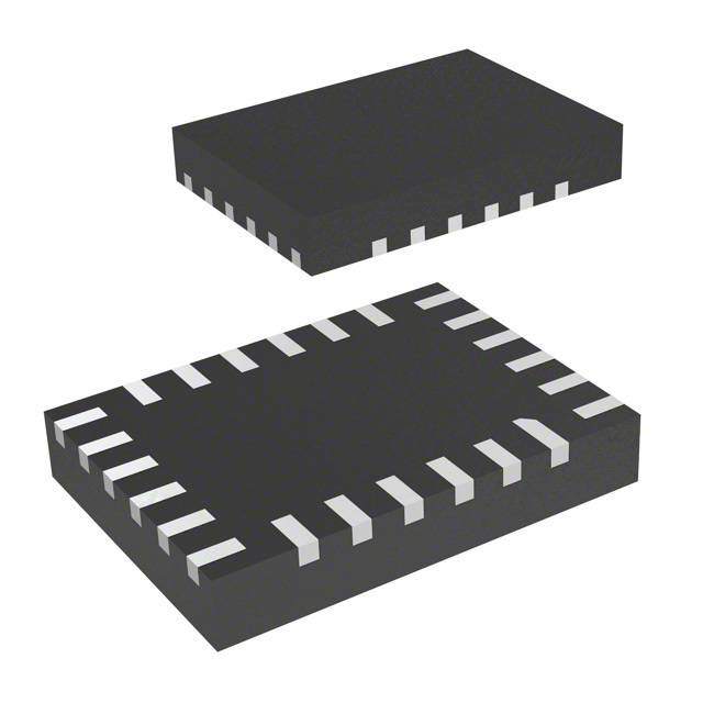
| 供应商器件封装 | 24-UMLP |
| 其它名称 | FSSD06UMX-ND |
| 包装 | 带卷 (TR) |
| 单位重量 | 29 mg |
| 商标 | Fairchild Semiconductor |
| 安装类型 | 表面贴装 |
| 安装风格 | SMD/SMT |
| 导通电阻—最大值 | 4 Ohms |
| 封装 | Reel |
| 封装/外壳 | 24-UMLP |
| 封装/箱体 | UMLP-24 |
| 工厂包装数量 | 5000 |
| 带宽 | 120 MHz |
| 应用 | 手机,数码相机,媒体播放器 |
| 开关电流—典型值 | 1 uA |
| 最大工作温度 | + 85 C |
| 最小工作温度 | - 40 C |
| 标准包装 | 5,000 |
| 电源电压-最大 | 3.6 V |
| 电源电压-最小 | 1.65 V |
| 类型 | 多路复用器 |
| 系列 | FSSD06 |


- 商务部:美国ITC正式对集成电路等产品启动337调查
- 曝三星4nm工艺存在良率问题 高通将骁龙8 Gen1或转产台积电
- 太阳诱电将投资9.5亿元在常州建新厂生产MLCC 预计2023年完工
- 英特尔发布欧洲新工厂建设计划 深化IDM 2.0 战略
- 台积电先进制程称霸业界 有大客户加持明年业绩稳了
- 达到5530亿美元!SIA预计今年全球半导体销售额将创下新高
- 英特尔拟将自动驾驶子公司Mobileye上市 估值或超500亿美元
- 三星加码芯片和SET,合并消费电子和移动部门,撤换高东真等 CEO
- 三星电子宣布重大人事变动 还合并消费电子和移动部门
- 海关总署:前11个月进口集成电路产品价值2.52万亿元 增长14.8%


PDF Datasheet 数据手册内容提取
Is Now Part of To learn more about ON Semiconductor, please visit our website at www.onsemi.com Please note: As part of the Fairchild Semiconductor integration, some of the Fairchild orderable part numbers will need to change in order to meet ON Semiconductor’s system requirements. Since the ON Semiconductor product management systems do not have the ability to manage part nomenclature that utilizes an underscore (_), the underscore (_) in the Fairchild part numbers will be changed to a dash (-). This document may contain device numbers with an underscore (_). Please check the ON Semiconductor website to verify the updated device numbers. The most current and up-to-date ordering information can be found at www.onsemi.com. Please email any questions regarding the system integration to Fairchild_questions@onsemi.com. ON Semiconductor and the ON Semiconductor logo are trademarks of Semiconductor Components Industries, LLC dba ON Semiconductor or its subsidiaries in the United States and/or other countries. ON Semiconductor owns the rights to a number of patents, trademarks, copyrights, trade secrets, and other intellectual property. A listing of ON Semiconductor’s product/patent coverage may be accessed at www.onsemi.com/site/pdf/Patent-Marking.pdf. ON Semiconductor reserves the right to make changes without further notice to any products herein. ON Semiconductor makes no warranty, representation or guarantee regarding the suitability of its products for any particular purpose, nor does ON Semiconductor assume any liability arising out of the application or use of any product or circuit, and specifically disclaims any and all liability, including without limitation special, consequential or incidental damages. Buyer is responsible for its products and applications using ON Semiconductor products, including compliance with all laws, regulations and safety requirements or standards, regardless of any support or applications information provided by ON Semiconductor. “Typical” parameters which may be provided in ON Semiconductor data sheets and/or specifications can and do vary in different applications and actual performance may vary over time. All operating parameters, including “Typicals” must be validated for each customer application by customer’s technical experts. ON Semiconductor does not convey any license under its patent rights nor the rights of others. ON Semiconductor products are not designed, intended, or authorized for use as a critical component in life support systems or any FDA Class 3 medical devices or medical devices with a same or similar classification in a foreign jurisdiction or any devices intended for implantation in the human body. Should Buyer purchase or use ON Semiconductor products for any such unintended or unauthorized application, Buyer shall indemnify and hold ON Semiconductor and its officers, employees, subsidiaries, affiliates, and distributors harmless against all claims, costs, damages, and expenses, and reasonable attorney fees arising out of, directly or indirectly, any claim of personal injury or death associated with such unintended or unauthorized use, even if such claim alleges that ON Semiconductor was negligent regarding the design or manufacture of the part. ON Semiconductor is an Equal Opportunity/Affirmative Action Employer. This literature is subject to all applicable copyright laws and is not for resale in any manner.
F S S D 0 March 2012 6 — S D / S FSSD06 — SD/SDIO and MMC Two-Port Multiplexer D I O a Features Description n d On Resistance Typically 4Ω, V =2.7V The FSSD06 is a two-port multiplexer that allows Secure M DDH Digital (SD), Secure Digital I/O (SDIO), and Multimedia M ftoggle: > 120MHz Card (MMC) host controllers to be expanded out to C Low On Capacitance: 9pF Typical multiple cards or peripherals. This configuration enables T the CMD, CLK, and D[3:0] signals to be multiplexed to w Low Power Consumption: 1µA Maximum dual-card peripherals. It is optimized for 1-bit / 4-bit SD / o - Conforms to Secure Digital (SD), Secure Digital I/O MMC applications. P o (SDIO), and Multimedia Card (MMC) Specifications The architecture includes the necessary bi-directional r t Supports 1-Bit / 4-Bit Host Controllers (V =1.65V to data and command transfer capability for single high- M DDH 3.6V) Communicating with High-Voltage (2.7-3.6V) voltage cards or dual-voltage supply cards. The clock u l and Dual-Voltage Cards (1.65-1.95V, 2.7-3.6V) path for the FSSD06 is a uni-directional buffer with an ti p integrated pull-up for high-impedance mode. - V =1.65 to 3.6V, V =V to 3.6V le DDH DDC1/C2 DDH Typical applications involve switching in portables and x 24-Lead MLP (3.5 x 4.5mm) and UMLP Packages e consumer applications: cell phones, digital cameras, r home theater monitors, portable GPS units, and printers. Applications Cell Phone, PDA, Digital Camera, Portable GPS LCD Monitor, Home Theater PC/TV, All-in-One Printer Analog Symbol Diagram VDDC1 VDDC2 Control /SOE VDDH 5 1DAT[0:3], 1CMD 5 DAT[0:3], CMD 5 2DAT[0:3], 2CMD VDDC1 VDDC2 RPU RPU CLK 1CLK 2CLK GND Figure 1. Analog Symbol Diagram Ordering Information Operating Packing Part Number Package Description Temperature Range Method 24-Lead Molded Leadless Package (MLP), JEDEC MO- FSSD06BQX -40°C to +85°C Tape & Reel 220, 3.5 x 4.5mm FSSD06UMX -40°C to +85°C 24-Lead Ultrathin Molded Leadless Package (UMLP) Tape & Reel © 2007 Fairchild Semiconductor Corporation www.fairchildsemi.com FSSD06 • Rev. 1.0.5
F S S Pin Configuration D 0 6 2] 3] — /OE 1DAT[ 1DAT[ 1CMD DAT[2] /OE 1DAT[2] 1DAT[3] 1CMD VDDC1 SD/ 2 1 24 23 S 24 23 22 21 20 19 D DAT[2] 3 22 VDDC1 IO DAT[3] 1 18 1CLK DAT[3] 4 21 1CLK a CMD 5 20 1DAT[0] CMD 2 17 1DAT[0] nd M VDDH 6 19 1DAT[1] VDDH 3 16 1DAT[1] M GND 7 18 2DAT[2] GND 4 15 2DAT[2] C T CLK 8 17 2DAT[3] CLK 5 14 2DAT[3] w o DAT[0] 9 16 2CMD - DAT[0] 6 13 2CMD P DAT[1] 10 15 VDDC2 o r 11 12 13 14 7 8 9 10 11 12 t M S 2DAT[1] 2DAT[0] 2CLK DAT[1] S 2DAT[1] 2DAT[0] 2CLK VDDC2 ultiple Figure 2. MLP Pin Assignments Figure 3. UMLP Pin Assignments x e r Pin Definitions Name Description VDDH Power Supply (Host ASIC) VDDC1, VDDC2 Power Supply (SDIO Peripheral Card Ports) /OE Output Enable (Active Low) S Select Pin 1DAT[3:0], 2DAT[3:0], 1CMD, 2CMD SDIO Card Ports DAT[3:0], CMD SDIO Common Ports CLK, 1CLK, 2CLK Clock Path Ports Truth Table /OE S Function LOW LOW CMD, CLK, DAT[3:0] connected to 1CMD, 1CLK, 1DAT[3:0]; 2CLK pulled HIGH via R PU LOW HIGH CMD, CLK, DAT[3:0] connected to 2CMD, 2CLK, 2DAT[3:0]; 1CLK pulled HIGH via R PU HIGH X All Ports High Impedance; 1CLK, 2CLK pulled HIGH via R PU © 2007 Fairchild Semiconductor Corporation www.fairchildsemi.com FSSD06 • Rev. 1.0.5 2
F S Typical Application Diagram S D VDDH 0 VDDC1 6 1.65–3.60V FSSD06 — V to3.6V RT DDH S D CMD, DAT[3:0] GND WiFi, /S 1CMD,1DAT[3:0] Bluetooth, D 5 5 MMCorSD IO Processor 1CLK Module a n Secure Data / VDDC2 d CLK Multimedia Card M 2:1 Peripheral RT VDDHto3.6V M Expander C Note: External resistors (RT) are GND T recommended if card supplies are 2CMD,2DAT[3:0] w allowed to float in the application. 5 WiFi,,, o- The resistors should be >500K to Bluetooth, P minimize power consumption. MMCorSD o 2CLK Module rt GND /OE M S u l t Figure 4. Typical Application Diagram ip l e x Functional Description e r The FSSD06 enables sharing the ASIC/baseband CLK Bus processor SDIO port(s) to two peripheral cards, The 1CLK and 2CLK outputs are bi-state buffer providing bi-directional support for dual-voltage architectures, rather than a switch I/O, to ensure 52MHz SD/SDIO or MMC cards available in the marketplace. incident wave switching. When there is no Each SDIO port of the FSSD06 has its own supply rail, communication on the bus (IDLE), the FSSD06 can be allowing peripheral cards with different supplies to be disabled with the /OE pin. When this pin is pulled HIGH, interfaced to the host. The peripheral card supplies must the nCLK outputs are also pulled HIGH. Along with be equal or greater than the host to minimize power nCMD, nDAT[3:0] goes high-impedance to ensure that consumption. The independent V , V , and V DDH DDC1 DDC2 the CLK path between the FSSD06 and the peripheral are defined by the supplies connected from the does not float. application Power Management ICs (PMICs) to the FSSD06. The clock path is a uni-directional buffered path rather than a bi-directional switch port. IDLE State CMD/DAT Bus “Parking” The SD and MMC card specifications were written for a CMD, DAT Bus Pull-ups direct point-to-point communication between host controller and card. The introduction of the FSSD06 in The 1CMD, 2CMD, 1DAT[3:0], and 2DAT[3:0] ports do that path, as an expander, requires that the functional not have, internally, the system pull-up resistors as operation and system latency not be impacted by the defined in the MMC or SD card system bus FSSD06 switch characteristics. Since there are various specifications. The system bus pull-up must be added card formats, protocols, and configurable controllers, a external to the FSSD06. The value, within the specific /OE pin is available to facilitate a fast IDLE transition for specification limits, is a function of the individual the nCMD/nDAT[3:0] outputs. Some controllers, rather application and type of card or peripheral connected. For than simply placing CMD/DAT into high-impedance SD card applications, the R and R pull-ups should CMD DAT mode, may pull their outputs HIGH for a clock cycle prior be between 10kΩ and 100kΩ. For MMC applications, to going into high-impedance mode (referred to as the R pull-ups should be between 4.7kΩ and 100kΩ CMD “parking” the output). Some legacy controllers pull their and the R pull-ups between 50kΩ and 100kΩ. The DAT outputs HIGH versus high impedance. card-side 1CMD, 2CMD, 1DAT[3:0], and 2DAT[3:0] outputs have a circuit that facilitates incident wave If the /OE pin is left LOW and the controller places the switching, so the external pull-up resistors ensure CMD/DAT[3:0] outputs into high impedance, the retention of the output high level. nCMD/nDAT[3:0] output rise time is a function of the RC time constant through the switch path. It is The /OE pin can be used to place the 1CMD, 2CMD, recommended that the host controller pull CMD and 1DAT[3:0] and 2DAT[3:0] into high-impedance mode DAT[3:0] HIGH for one cycle before pulling /OE HIGH. when the system enters IDLE state (see IDLE State This facilitates parking all nCMD/nDAT[3:0] outputs CMD/DAT Bus “Parking”). HIGH before putting the switch I/Os in high impedance. © 2007 Fairchild Semiconductor Corporation www.fairchildsemi.com FSSD06 • Rev. 1.0.5 3
F S Absolute Maximum Ratings S D Stresses exceeding the absolute maximum ratings may damage the device. The device may not function or be 0 6 operable above the recommended operating conditions and stressing the parts to these levels is not recommended. — In addition, extended exposure to stresses above the recommended operating conditions may affect device reliability. The absolute maximum ratings are stress ratings only. S D / Symbol Parameter Conditions Min. Max. Unit S D V Supply Voltage -0.5 4.6 V I DDH O VDDC1,VDDC2 Supply Voltage -0.5 4.6 V a n 1DAT[3:0], 2DAT[3:0], 1CMD, V (2)+ 0.3V d 2CMD Pins -0.5 (4.6DVD xmaximum) V M V (1) Switch I/O Voltage SW V (2)+ 0.3V M DAT[3:0], CMD Pins -0.5 DDx V C (4.6V maximum) T V (1) Control Input Voltage S, /OE -0.5 4.6 V w CNTRL o VCLKI(1) CLK Input Voltage CLK -0.5 4.6 V -P V (2)+ 0.3V o VCLKO(1) CLK Output Voltage 1CLK, 2CLK -0.5 (4.6DVD xmaximum) V rt M I Input Clamp Diode Current -50 mA INDC u l ISW Switch I/O Current SDIO Continuous 50 mA tip l e SDIO Pulsed at 1ms Duration, I Peak Switch Current 100 mA x SWPEAK <10% Duty Cycle e r T Storage Temperature Range -65 +150 C STG T Max Junction Temperature +150 C J T Lead Temperature Soldering, 10 Seconds +260C C L I/O to GND 8 Human Body Model Supply to GND 9 kV (JEDEC: JESD22-A114) ESD All Other Pins 5 Charged Device Model (JEDEC: JESD22-C101) 2 kV Notes: 1. The input and output negative ratings may be exceeded if the input and output diode current ratings are observed. 2. V references the specific SDIO port V rail (i.e. V , V , V ). DDx DD DDC1 DDC2 DDH Recommended Operating Conditions The Recommended Operating Conditions table defines the conditions for actual device operation. Recommended operating conditions are specified to ensure optimal performance to the datasheet specifications. Fairchild does not recommend exceeding them or designing to Absolute Maximum Ratings. Symbol Parameter Minimum Maximum Unit V Supply Voltage - Host Side 1.65 3.6V V DDH V V Supply Voltage - SDIO Cards V 3.6V V DDC1, DDC2 DDH V Control Input Voltage - V ,V 0 V V CNTRL S /OE DDH V Clock Input Voltage - V 0 V V CLKI CLKI DDH Switch I/O Voltage - CMD, DAT[3:0] 0 V V DDH V Switch I/O Voltage - 1CMD, 1DAT[3:0] 0 V V SW DDC1 Switch I/O Voltage - 2CMD, 2DAT[3:0] 0 V V DDC2 °C Operating Temperature -40 +85 °C Thermal Resistance (free air), MLP24 50 °C/W JA © 2007 Fairchild Semiconductor Corporation www.fairchildsemi.com FSSD06 • Rev. 1.0.5 4
F S DC Electrical Characteristics at 1.8V VDDH S D All typical values are for V =1.8V at 25°C unless otherwise specified. 0 DDH 6 — T =- 40°C to +85°C V / A Symbol Parameter DDC1 Conditions Unit S V (V) DDC2 Min. Typ. Max. D / S Common Pins D I V Clamp Diode Voltage 2.7 I -18mA -1.2 O IK IK= a Control Input Voltage V 2.7 1.3 V n IH High V =1.65V d DDH M V Control Input Voltage Low 2.7 0.5 IL M I S, /OE Input High Current 3.6 VDDH=1.95V, VCNTRL=0V to -1 1 µA C IN V DDH T w Off Leakage, Current of I 3.6 V =1.95V, V =0V to V -1.0 0.5 1.0 µA o OZ all ports DDH SW DDX - P V =V V =0V, o IPU CLK Pull-up Current 3.6 /OCELK=IVDDDDHH CLKO 35 µA rt M V CLK Output Voltage High 2.7 I =-2mA 2.4 V OHC OH u l VOLC CLK Output Voltage Low 3.6 IOL=-2mA 90 mV tip RPU CLK Pull-up Resistance(3) 50 100 kΩ le x RON Switch On Resistance(4) 2.7 VSeCMeD F, DigAuT[r3e:0 ]5=0 V, ION=-2mA, 4 6 Ω er ∆R Delta On Resistance(4, 5) 2.7 V 0V, I - 2mA 0.8 Ω ON CMD, DAT[3:0]= ON= Power Supply Quiescent Supply Current V =1.95V, V 0 or V , I 0 DDH SW= DDH 1 µA CC(VDDH) (Host) I =0 OUT V 0 or V I =0, I Quiescent Supply Current SW= DDx, OUT CC(VDDC1, 3.6 V =V , V =Open, 1 µA (SDIO Cards) CLKI DDH CLKO VDDC2) /OE=0V V 0 or V I =0, Delta I for 3.6V SW= DDx, OUT ∆I CC(VDDC1, VDDC2) V =V , V =Open, 1 µA CARD One Card Powered Off / 0V CLKI DDH CLKO /OE=0V Notes: 3. Guaranteed by characterization, not production tested. 4. On resistance is determined by the voltage drop between the switch I/O pins at the indicated current through the switch. 5. ∆ R =R – R measured at identical V , temperature, and voltage. ON ON max ON min CC © 2007 Fairchild Semiconductor Corporation www.fairchildsemi.com FSSD06 • Rev. 1.0.5 5
F S DC Electrical Characteristics at 2.7V VDDH S D All typical values are for V =2.7V at 25°C unless otherwise specified. 0 DDH 6 — T =- 40°C to +85°C V / A Symbol Parameter DDC1 Conditions Unit S V (V) DDC2 Min. Typ. Max. D / S Common Pins D I V Clamp Diode Voltage 2.7 I -18mA -1.2 O IK IK= a Control Input Voltage V 2.7 1.8 V n IH High V =2.7V d DDH M V Control Input Voltage Low 2.7 0.8 IL M I S, /OE Input High Current 3.6 VDDH=3.6V, VCNTRL=0V to -1 1 µA C IN V DDH T w I Off Leakage Current of all V =3.6V, V =0V to V OZ 3.6 DDH SW DDX -1.0 0.5 1.0 µA o ports - P I CLK Pull-up Current V =V V =0V, o PU 3.6 CLKI DDH, CLKO 50 µA r /OE=VDDH t M V CLK Output Voltage High 2.7 I =-2mA 2.4 V OHC OH u l VOLC CLK Output Voltage Low 3.6 IOL=-2mA 90 mV tip RPU CLK Pull-up Resistance(6) 50 100 kΩ le x RON Switch On Resistance(7) 2.7 VSeCMeD F, DigAuT[r3e:0 ]5=0 V, ION=-2mA 2.5 6.0 Ω er ∆R Delta On Resistance(7,8) 2.7 V 0V, I - 2mA 0.8 Ω ON CMD, DAT[3:0]= ON= Power Supply Quiescent Supply Current V =3.6V, V 0 or V , I 0 DDH SW= DDH 1 µA CC(VDDH) (Host) I =0 OUT V 0 or V I =0, I Quiescent Supply Current SW= DDx, OUT CC(VDDC1, 3.6 V =V , V =Open, 1 µA (SDIO Cards) CLKI DDH CLKO VDDC2) /OE=0V V 0 or V I =0, Delta I for 3.6V/0V SW= DDx, OUT ∆I CC(VDDC1, VDDC2) V =V , V =Open, 1 µA CARD One Card Powered Off 0V/3.6V CLKI DDH CLKO /OE=0V Notes: 6. Guaranteed by characterization, not production tested. 7. On resistance is determined by the voltage drop between the switch I/O pins at the indicated current through the switch. 8. ∆R =R – R measured at identical V , temperature, and voltage. ON ON max ON min CC © 2007 Fairchild Semiconductor Corporation www.fairchildsemi.com FSSD06 • Rev. 1.0.5 6
F S AC Electrical Characteristics at 1.8V VDDH S D All typical values are for V 1.8V at 25°C unless otherwise specified. 0 DDH= 6 — T =- 40°C to +85°C V / A Symbol Parameter DDC1 Conditions Unit S V (V) DDC2 Min. Typ. Max. D / S Turn-On Time, V =0V, R =1kΩ, C =30pF t 2.7 to 3.6 SW L L 10 24 ns D ON1 S, /OE to CMD, DAT[3:0] See Figure 7, Figure 8 I O Turn-Off Time, V =0V, R =1kΩ, C =30pF t 2.7 to 3.6 SW L L 7 22 ns a OFF1 S, /OE to CMD, DAT[3:0] See Figure 7, Figure 8 n d Switch Propagation t 2.7 to 3.6 See Figure 9 1 ns M PD Delay(9) M Switch Skew(9, 10) C tSKEW CMD, DAT[3:0] 2.7 to 3.6 RL=1kΩ, CL=30pF 2 ns T w t Turn-On Time, 2.7 to 3.6 VSW=0V, RL=1kΩ, CL=30pF 17 35 ns o ON2 S, /OE to 1CLK, 2CLK See Figure 7, Figure 8 -P o Turn-Off Time V =0V, R =1kΩ, C =30pF tOFF2 S, /OE to 1CLK, 2CLK 2.7 to 3.6 SeSWe FigureL 7, FigureL 8 10 28 ns rt M R =1kΩ, C =30pF u tPDCLK Clock Propagation Delay 2.7 to 3.6 SeLe FigureL 11 3.0 5.5 ns lt i p f=10MHz, R 50Ω, C =30pF, l O Off Isolation(9) 2.7 to 3.6 T= L -60 dB e IRR See Figure 12 x e Xtalk Non-Adjacent Channel 2.7 to 3.6 f=10MHz, RT=50Ω, CL=30pF, -60 dB r Crosstalk(9) See Figure 13 f Clock Frequency(9) 2.7 to 3.6 C =30pF 120 MHz toggle L Notes: 9. Guaranteed by characterization, not production tested. 10. Skew is determined by |T - T | for worst-case temperature and V . PLH PHL DDX © 2007 Fairchild Semiconductor Corporation www.fairchildsemi.com FSSD06 • Rev. 1.0.5 7
F S AC Electrical Characteristics at 2.7V VDDH S D All typical values are for V =2.7V at 25°C unless otherwise specified. 0 DDH 6 — T =- 40°C to +85°C V / A Symbol Parameter DDC1 Conditions Unit S V (V) DDC2 Min. Typ. Max. D / S Turn-On Time V =0V, R =1kΩ, C =30pF t 2.7 to 3.6 SW L L 8 17 ns D ON1 S, /OE to CMD, DAT[3:0] See Figure 7, Figure 8 I O Turn-Off Time V =0V, R =1kΩ, C =30pF t 2.7 to 3.6 SW L L 6 13 ns a OFF1 S, /OE to CMD, DAT[3:0] See Figure 7, Figure 8 n d Switch Propagation t 2.7 to 3.6 See Figure 9 1 ns M PD Delay(11) M Switch Skew(12) C tSKEW CMD, DAT[3:0] 2.7 to 3.6 RL=1kΩ, CL=30pF 1.5 ns T w t Turn-On Time 2.7 to 3.6 VSW=0V, RL=1kΩ, CL=30pF 15 25 ns o ON2 S, /OE to 1CLK, 2CLK See Figure 7, Figure 8 -P o Turn-Off Time V =0V, R =1kΩ, C =30pF tOFF2 S, /OE to 1CLK, 2CLK 2.7 to 3.6 SeSWe FigureL 7, FigureL 8 10 25 ns rt M R =1kΩ, C =30pF u tPDCLK Clock Propagation Delay 2.7 to 3.6 SeLe FigureL 11 1.5 3.0 ns lt i p f=10MHz, R 50Ω, C =30pF l O Off Isolation(11) 2.7 to 3.6 T= L -60 dB e IRR See Figure 12 x e Xtalk Non-Adjacent Channel 2.7 to 3.6 f=10MHz, RT=50Ω, CL=30pF -60 dB r Crosstalk(11) See Figure 13 f Clock Frequency(11) 2.7 to 3.6 C =30pF 120 MHz toggle L Notes: 11. Guaranteed by characterization, not production tested. 12. Skew is determined by |T - T | for worst-case temperature and V . PLH PHL DDX Capacitance T =- 40°C to +85°C A Symbol Parameter Conditions Unit Min. Typ. Max. Control and CLK Pin Input C V 0V 2.5 IN (S, /OE, CLK) Capacitance DDH= V 1.8V,V V 2.7V, Common Port On Capacitance DDH= DDC1= DDC2= C V 0V, V =0V, f=1MHz 9.0 ON (C ) /OE= bias pF DAT[3:0], CMD See Figure 15 V 1.8V,V V 2.7V, DDH= DDC1= DDLH2= C Input Source Off Capacitance V 3.3V, V =0V, f=1MHz 4.0 OFF /OE= bias See Figure 14 © 2007 Fairchild Semiconductor Corporation www.fairchildsemi.com FSSD06 • Rev. 1.0.5 8
F S Test Diagrams S D 0 6 VV — OONN S D NC IIOOZZ /S nDAT[3:0],nCMD DDAATT[[33::00]],,CCMMDD A D I O VVVIIINNN VVVIIINNN a II Select n GGGGGNNNNNDDDDD SSeelleecctt OONN GGGGGNNNNNDDDDD d GGGNNNDDD V = 0 orVVddl M VV = 0 orVVddddll S M R = V / I SS C ON ON ON T w o Figure 5. On Resistance Figure 6. Off Leakage (Each Switch Port is - P Tested Separately) o r t M u V l DDx t i p l nDAT[3:0],nCMD DAT[3:0], tRISE=2.5ns tFALL=2.5ns ex CMD e R r L V ddx VSW 90% 90% GND RS CL VVOOUUTT Input--VC1N0TR%L Vddx/2 Vddx/2 10% GND GND V OH VVV S Output-VOUT 50% GNDR ,R ,andC arefunctionofapplication VOL tOVFoFl+0.15tVON L S L environment (seeACTablesforspecificvalues) C includestestfixtureandstraycapacitance L Figure 7. AC Test Circuit Load Figure 8. Turn On/Off Time Waveforms V DDx t =2.5ns tt =2.5ns RRIISSEE FFAALLLL CLK 1CLK, Vddx 2CLK RL 90% 90% V CCLLKKII Input---V VV S1W0% Vddx///222 VVddddxx//22 10% GND RRSS CL OOUUTT GGNNDD VOH GND Output---VOUT 50% 50% VS VVOL GND tppLLHH tppHHLL RL,RS,andCLarefunctionofapplication environment (seeACTablesforspecificvalues) C includestestfixtureandstraycapacitance L Figure 9. Switch Propagation Delay Waveform Figure 10. AC Test Circuit Load (CLK) © 2007 Fairchild Semiconductor Corporation www.fairchildsemi.com FSSD06 • Rev. 1.0.5 9
F S Test Diagrams (Continued) S D 0 6 tRISE=2.5ns tFALL=2.5ns NetworkAnalyzer — RRRSSS S Vddx D Input-VCLKI 90% 90% RT GND VVVIIINNN VS /S GND 10% Vddx/2 Vddx/2 10% VS GND GND DIO VOHC GND GND RRRTTTVOOUUTT an Output-VCLKO 50% 50% RSandRTarefunctionofapplication d environment (seeACTablesforspecificvalues) GGGGGGNNNNNNDDDDDD M VOLC tpLH tpHL Off--IIssoollaattiioonn==2200LLoogg((VVOOUUTT//VVIINN)) MC T Figure 11. CLK Propagation Delay Waveforms Figure 12. Channel Off Isolation w o -P o r t M u NetworkAnalyzer lt NC ip R S l e x V e GND IN VS r VS GND GND R T GND V GND R OUT T R andR arefunctionofapplicationenvironment S T (seeACTablesforspecificvalues) GND CROSSTALK=20Log(V /V ) OUT IN Figure 13. Channel-to-Channel Crosstalk nDAT[3:0],nCMD, nCLK Capacitance S Capacitance Meter S Meter VS= 0 orVddh f=1MHz,V =0V V = 0 orV bias S ddh f=1MHz,V =0V bias nDAT[3:0],nCMD,nCLK nDAT[3:0],nCMD,nCLK Figure 14. Channel Off Capacitance Figure 15. Channel On Capacitance © 2007 Fairchild Semiconductor Corporation www.fairchildsemi.com FSSD06 • Rev. 1.0.5 10
F S Tape and Reel Specifications S D 0 Package Cover Tape 6 Tape Selection Number Cavities Cavity Status Designator Status — Leader (Start End) 125 (Typical) Empty Sealed S D MPX Carrier 3000 Filled Sealed / S Trailer (Hub End) 75 (Typical) Empty Sealed D I O Tape Dimensions a n Dimensions are in millimeters unless otherwise noted. d M M C T w o - P o r t M u l t i p l e x e r Reel Dimensions Dimensions are in inches (millimeters) unless otherwise noted. Tape Size A B C D N W1 W2 13.000 0.059 0.512 0.795 2.165 0.488 0.724 (12.00mm) (330.00) (1.50) (13.00) (20.00) (55.00) (12.40) (18.40) © 2007 Fairchild Semiconductor Corporation www.fairchildsemi.com FSSD06 • Rev. 1.0.5 11
None
2.50±0.10 A B 0.663 19 24 PIN#1 0.563 IDENT 1 18 0.400 3.40±0.10 2.225 3.700 13 6 0.225 7 12 TOP VIEW 2.225 0.025±0.025 2.800 0.50±0.05 LAND PATTERN RECOMMENDATION SEATING PLANE C 0.50±0.05 SIDE VIEW - OPTION A 0.10±0.05 0.50±0.05 45° 0.20±0.05 SEATING PLANE C 0.025±0.025 SIDE VIEW - OPTION B DETAIL A 0.05 SCALE 2:1 (0.15) 4X POTENTIAL NOTES: PULL BACK 7 12 A. PACKAGE DOES NOT FULLY CONFORM TO JEDEC STANDARD B. ALL DIMENSIONS ARE IN MILLIMETERS 6 13 0.40 C. LAND PATTERN RECOMMENDATION IS EXISTING INDUSTRY LAND PATTERN D. DRAWING FILENAME: MKT-UMLP24ArevE DETAIL A 1 18 PIN#1 0.40±0.05 (23X) IDENT 24 19 0.20±0.05 (24X) 0.85 0.10 C A B BOTTOM VIEW 0.05 C
ON Semiconductor and are trademarks of Semiconductor Components Industries, LLC dba ON Semiconductor or its subsidiaries in the United States and/or other countries. ON Semiconductor owns the rights to a number of patents, trademarks, copyrights, trade secrets, and other intellectual property. A listing of ON Semiconductor’s product/patent coverage may be accessed at www.onsemi.com/site/pdf/Patent−Marking.pdf. ON Semiconductor reserves the right to make changes without further notice to any products herein. ON Semiconductor makes no warranty, representation or guarantee regarding the suitability of its products for any particular purpose, nor does ON Semiconductor assume any liability arising out of the application or use of any product or circuit, and specifically disclaims any and all liability, including without limitation special, consequential or incidental damages. Buyer is responsible for its products and applications using ON Semiconductor products, including compliance with all laws, regulations and safety requirements or standards, regardless of any support or applications information provided by ON Semiconductor. “Typical” parameters which may be provided in ON Semiconductor data sheets and/or specifications can and do vary in different applications and actual performance may vary over time. All operating parameters, including “Typicals” must be validated for each customer application by customer’s technical experts. ON Semiconductor does not convey any license under its patent rights nor the rights of others. ON Semiconductor products are not designed, intended, or authorized for use as a critical component in life support systems or any FDA Class 3 medical devices or medical devices with a same or similar classification in a foreign jurisdiction or any devices intended for implantation in the human body. Should Buyer purchase or use ON Semiconductor products for any such unintended or unauthorized application, Buyer shall indemnify and hold ON Semiconductor and its officers, employees, subsidiaries, affiliates, and distributors harmless against all claims, costs, damages, and expenses, and reasonable attorney fees arising out of, directly or indirectly, any claim of personal injury or death associated with such unintended or unauthorized use, even if such claim alleges that ON Semiconductor was negligent regarding the design or manufacture of the part. ON Semiconductor is an Equal Opportunity/Affirmative Action Employer. This literature is subject to all applicable copyright laws and is not for resale in any manner. PUBLICATION ORDERING INFORMATION LITERATURE FULFILLMENT: N. American Technical Support: 800−282−9855 Toll Free ON Semiconductor Website: www.onsemi.com Literature Distribution Center for ON Semiconductor USA/Canada 19521 E. 32nd Pkwy, Aurora, Colorado 80011 USA Europe, Middle East and Africa Technical Support: Order Literature: http://www.onsemi.com/orderlit Phone: 303−675−2175 or 800−344−3860 Toll Free USA/Canada Phone: 421 33 790 2910 Fax: 303−675−2176 or 800−344−3867 Toll Free USA/Canada Japan Customer Focus Center For additional information, please contact your local Email: orderlit@onsemi.com Phone: 81−3−5817−1050 Sales Representative © Semiconductor Components Industries, LLC www.onsemi.com www.onsemi.com 1
Mouser Electronics Authorized Distributor Click to View Pricing, Inventory, Delivery & Lifecycle Information: O N Semiconductor: FSSD06UMX FSSD06BQX