/KSZ8993.jpg)
 Datasheet下载
- 型号: KSZ8993
- 制造商: Micrel
- 库位|库存: xxxx|xxxx
- 要求:
| 数量阶梯 | 香港交货 | 国内含税 |
| +xxxx | $xxxx | ¥xxxx |
查看当月历史价格
查看今年历史价格
KSZ8993产品简介:
ICGOO电子元器件商城为您提供KSZ8993由Micrel设计生产,在icgoo商城现货销售,并且可以通过原厂、代理商等渠道进行代购。 KSZ8993价格参考¥33.04-¥33.04。MicrelKSZ8993封装/规格:专用 IC, 10/100 Integrated Switch IC Port Switch/Network Interface 128-PQFP (14x20)。您可以下载KSZ8993参考资料、Datasheet数据手册功能说明书,资料中有KSZ8993 详细功能的应用电路图电压和使用方法及教程。
KSZ8993是Microchip Technology公司生产的一款专用IC,属于以太网交换机芯片系列。它主要应用于需要小型化、低功耗且高性能的网络连接场景中,以下是其典型应用场景:

1. 工业自动化:KSZ8993可用于工业以太网设备中,如PLC(可编程逻辑控制器)、HMI(人机界面)和远程I/O模块等,提供稳定可靠的网络通信能力。

2. 物联网(IoT)设备:在智能家居、智能城市或工业物联网领域中,该芯片可以作为核心组件实现多设备互联,支持高效的数据传输与管理。

3. 嵌入式系统:适用于各种嵌入式计算平台,例如网络附加存储(NAS)、IP摄像机、打印机服务器以及其他需要内置网络功能的小型化设备。

4. 消费电子产品:包括游戏机、媒体播放器等需要高速网络接入的产品,能够通过KSZ8993实现更便捷的联网体验。

5. 汽车电子:随着车联网技术的发展,此款芯片也可用于车载信息娱乐系统及ADAS(高级驾驶辅助系统)中,确保车内各子系统间的数据交换顺畅无阻。

6. 通信基础设施:小型基站、无线接入点或其他轻量级网络设施可能也会采用此类交换机芯片来构建基础架构。

总之,KSZ8993凭借其紧凑的设计、灵活配置以及强大的性能表现,非常适合那些对成本敏感但又要求较高网络性能的应用场合。
| 参数 | 数值 |
| 产品目录 | 集成电路 (IC)半导体 |
| 描述 | IC SWITCH 10/100 3PORT 128PQFP以太网 IC 3 Port 10/100 Switch w/Tranceivers & Frame Buffers, 128-Ld PQFP - Lead free |
| 产品分类 | |
| 品牌 | Micrel |
| 产品手册 | |
| 产品图片 |
|
| rohs | 符合RoHS无铅 / 符合限制有害物质指令(RoHS)规范要求 |
| 产品系列 | 通信及网络 IC,以太网 IC,Micrel KSZ8993- |
| 数据手册 | |
| 产品型号 | KSZ8993 |
| 产品 | Ethernet Switches |
| 产品目录页面 | |
| 产品种类 | 以太网 IC |
| 以太网连接类型 | 10Base-T, 100Base-FX, 100Base-TX |
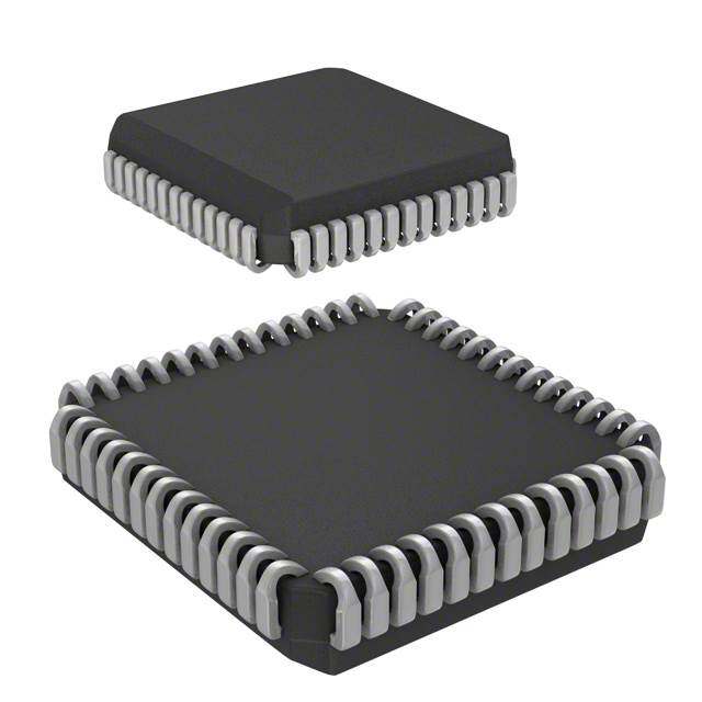
| 供应商器件封装 | 128-PQFP(14x20) |
| 其它名称 | 576-1032 |
| 包装 | 托盘 |
| 商标 | Micrel |
| 安装类型 | 表面贴装 |
| 安装风格 | SMD/SMT |
| 封装 | Tray |
| 封装/外壳 | 128-BFQFP |
| 封装/箱体 | PQFP-128 |
| 工厂包装数量 | 66 |
| 应用 | 端口开关/网络接口 |
| 接口 | MII, SNI |
| 收发器数量 | 3 Transceiver |
| 数据速率 | 10 Mb/s, 100 Mb/s |
| 最大工作温度 | + 70 C |
| 最大电源电流 | 330 mA |
| 最小工作温度 | 0 C |
| 标准包装 | 66 |
| 电源电压-最大 | 2.75 V, 3.6 V |
| 电源电压-最小 | 2.35 V, 3 V |
| 类型 | Integrated Switch |
| 系列 | KSZ8993 |


- 商务部:美国ITC正式对集成电路等产品启动337调查
- 曝三星4nm工艺存在良率问题 高通将骁龙8 Gen1或转产台积电
- 太阳诱电将投资9.5亿元在常州建新厂生产MLCC 预计2023年完工
- 英特尔发布欧洲新工厂建设计划 深化IDM 2.0 战略
- 台积电先进制程称霸业界 有大客户加持明年业绩稳了
- 达到5530亿美元!SIA预计今年全球半导体销售额将创下新高
- 英特尔拟将自动驾驶子公司Mobileye上市 估值或超500亿美元
- 三星加码芯片和SET,合并消费电子和移动部门,撤换高东真等 CEO
- 三星电子宣布重大人事变动 还合并消费电子和移动部门
- 海关总署:前11个月进口集成电路产品价值2.52万亿元 增长14.8%


PDF Datasheet 数据手册内容提取
KS8993 Micrel KS8993 3-Port 10/100 Integrated Switch with PHY and Frame Buffer Rev. 2.06 General Description The KS8993 has rich features such as VLAN and priority queuing and is designed to reside in an unmanaged design The KS8993 contains three 10/100 physical layer transceiv- not requiring processor intervention. This is achieved through ers, three MAC (Media Access Control) units with an inte- I/O strapping at system reset time. grated layer 2 switch. The device runs in two modes. The first On the media side, the KS8993 supports 10BaseT, mode is a three port integrated switch and the second is as 100BaseTX and 100BaseFX as specified by the IEEE 802.3 a three port switch with the third port decoupled from the committee. physical port. In this mode access to the third MAC is provided using a reverse or forward MII (Media Independent Interface) Physical signal transmission and reception are enhanced such that an external MAC can be directly connected to the through use of analog circuitry that makes the design more KS8993. This interface also supports the 7-wire (serial net- efficient and allows for lower power consumption and smaller work interface) as used by some routing devices. chip die size. Useful configurations include a stand alone three port switch Data sheets and support documentation can be found on as well as a two port switch with a routing element connected Micrel’s web site at www.micrel.com. to the extra MII port. The additional port is also useful for public network interfacing. Functional Diagram Look-Up SRAM Queue Buffer Engine Buffers Management Management (1K Entries) (16Kx32) FIFO and Flow Control MRXD[3:0] MRXDV MAC MAC MAC MCOL 1 2 3 MCRS M MRXCLK I I MTXD[3:0] MTXEN MTXER MII / SNI MTXCLK (exclusive) MCOLIN External Interface MRXD[0] MRXDV Physical Physical Physical MCOL Transceiver Transceiver Transceiver S MRXCLK N 1 2 3 I MTXD[0] MTXEN MTXCLK M[1] M[1] M[2] M[2] M[3] M[3] X X X X X X R T R T R T 1], 1], 2], 2], 3], 3], P[ P[ P[ P[ P[ P[ X X X X X X R T R T R T LED and LED[1][3:0] LED[2][3:0] Programming LED[3][3:0] Interface Micrel, Inc. • 2180 Fortune Drive • San Jose, CA 95131 • USA • tel + 1 (408) 944-0800 • fax + 1 (408) 474-1000 • http://www.micrel.com April 2009 1 KS8993
KS8993 Micrel Features Ordering Information • 3-port 10/100 integrated switch with physical layer Part Number Temperature transceivers Package • 64k Byte of SRAM on chip for frame buffering Standard Pb-Free Range • 1.0Gbps high performance memory bandwidth KS8993 KSZ8993 0°C to +70°C 128-Pin PQFP • 10BaseT, 100BaseTX and 100BaseFX modes of operation • Support for UTP or fiber installations • Superior analog technology for reduced power and die size • Supports port based VLAN • QoS feature!! Supports 802.1p based priority or port- based priority • Indicators for link, activity, full/half-duplex and speed • Unmanaged operation via strapping at system reset time • Hardware based 10/100, full/half, flow control and auto- negotiation • Individual port forced modes (full-duplex, 100BaseTX) when auto-negotiation is disabled • Wire speed reception and transmission • On chip integrated address look-up engine, supports 1K absolute MAC addresses • Automatic address learning, address aging and address migration • Full-duplex IEEE 802.3x flow control (Pause) with force mode option • Half-duplex back pressure flow control • Comprehensive LED support • External MAC interface (MII or SNI 7-wire ) for router applications • 300mA (0.75W) including physical transmit drivers • Commercial temperature range: 0°C to +70°C • Available in 128-pin PQFP with single 2.5V power supply KS8993 2 April 2009
KS8993 Micrel Revision History Revision Date Summary of Changes 1.00 04/13/00 Document origination 1.01 05/31/00 Miscellaneous changes 1.02 06/08/00 Index repair 1.03 09/20/00 MII forward correction. MRXD[3:1] correction. 1.04 10/30/00 Update voltage ratings. 1.05 10/31/00 Correct I/O descriptions. 1.06 11/08/00 Correct mode operation for LED[1:3][0] Add timing information 1.07 12/21/00 Correct pin information 1.08 03/23/01 Correct VLAN description. 1.09 03/26/01 Update MODESEL descriptions for packet size extensions 1.10 04/19/01 Update electrical characteristics; Correct I/O information. 1.11 04/20/01 Correct timing information 1.12 05/10/01 Update I/O descriptions 1.13 06/08/01 Define control for LED[3][3] 1.14 06/26/01 Revise definition for LED[3][3] 1.15 08/1/01 Update timing information and power dissipation Add power up timing description; Correct DISAN3 default mode. 1.16 08/9/01 Correct LED [1] [1] to float configuration Add Reverse and Forward MII timing 2.00 4/8/02 Correct reserve buffer from 128 to 96 for PRSV pin. Add max. current. Add force flow control Option as follows: Change pin 50 from reserved to FFLOW1# for force flow control on port 1.) Change pin 46 from reserved to FFLOW2# for force flow control on port 2. Modify LED[1][2] for force flow control on port 3. 2.01 5/6/02 Add TX Disable for Port 1 and port 2, Power down for port 3 and Far end Fault Disable features using MUX[1:2] and TEST[1:2] pins. 2.02 7/2/02 Recommend pull-down on LED[3][3] 2.03 8/29/03 Convert to new format. 2.04 1/24/05 Added reset circuit recommendation. 2.05 5/12/05 Added lead-free part number April 2009 3 KS8993
KS8993 Micrel Table of Contents System Level Applications..............................................................................................................................................................5 Pin Description ..............................................................................................................................................................................6 I/O Grouping ..............................................................................................................................................................................9 I/O Descriptions ............................................................................................................................................................................10 Pin Configuration...........................................................................................................................................................................15 Functional Overview: Physical Layer Transceiver.....................................................................................................................16 100BaseTX Transmit...............................................................................................................................................................16 100BaseTX Receive................................................................................................................................................................16 PLL Clock Synthesizer ............................................................................................................................................................16 Scrambler/De-scrambler (100BaseTX only)............................................................................................................................16 100BaseFX operation..............................................................................................................................................................16 100BaseFX Signal Detection...................................................................................................................................................16 100BaseFX Far End Fault.......................................................................................................................................................16 10BaseT Transmit...................................................................................................................................................................16 10BaseT Receive....................................................................................................................................................................16 Power Management ................................................................................................................................................................17 LED Mode Selection................................................................................................................................................................17 Auto-Negotiation......................................................................................................................................................................17 Functional Overview: Switch Core...............................................................................................................................................18 Address Look Up.....................................................................................................................................................................18 Learning..........................................................................................................................................................................18 Migration.........................................................................................................................................................................18 Aging ............................................................................................................................................................................18 Forwarding......................................................................................................................................................................18 Switching Engine.....................................................................................................................................................................18 MAC (Media Access Controller) Operation .............................................................................................................................18 Inter Packet Group..........................................................................................................................................................18 Back off Algorithm...........................................................................................................................................................18 Late Collision ..................................................................................................................................................................18 Illegal Frame...................................................................................................................................................................18 Flow Control....................................................................................................................................................................18 Full-Duplex Flow Control.................................................................................................................................................18 Half-Duplex Back Pressure.............................................................................................................................................18 VLAN Support..........................................................................................................................................................................19 QoS Priority Support................................................................................................................................................................20 MII Interface Operation..................................................................................................................................................................21 SNI Interface (7-wire) Operation ...................................................................................................................................................22 Absolute Maximum Ratings..........................................................................................................................................................23 Operating Ratings..........................................................................................................................................................................23 Electrical Characteristics..............................................................................................................................................................23 Timing Diagrams............................................................................................................................................................................24 Reference Circuit ...........................................................................................................................................................................29 4B/5B Coding ............................................................................................................................................................................31 MLT Coding ............................................................................................................................................................................32 802.1q VLAN and 802.1p Priority Frame......................................................................................................................................33 Selection of Isolation Transformers.............................................................................................................................................34 Selection of Reference Crystals...................................................................................................................................................34 Package Outline and Dimensions ................................................................................................................................................35 KS8993 4 April 2009
KS8993 Micrel System Level Applications public network access. The major benefits of using the KS8993 are the lower power consumption, unmanaged op- The KS8993 can be configured to fit either in a three port 10/ eration, flexible configuration and built in frame buffering. 100 application or as a two port 10/100 network interface with Two such applications are depicted below. an extra MII or SNI port. This MII/SNI port can be connected to an external processor and used for routing purposes or Public Network Access Routing Engine KS8993 KS8993 3-Port 3-Port Switch Switch with with PHY PHY 3X 2X Transformer Transformer or Fiber or Fiber Interface Interface Or 2-Port with Public 3-Port Stand Alone Network Interface Figure 1. KS8993 Applications April 2009 5 KS8993
KS8993 Micrel Pin Description Pin Number Pin Name Type(Note 1) Port Pin Function 1 GND_ANA GND Analog ground 2 MUX[2] I Factory test pin 3 MUX[1] I Factory test pin 4 GND_RX[1] GND 1 Ground for receiver 5 RXP[1] I 1 Physical receive signal + (differential) 6 RXM[1] I 1 Physical receive signal - (differential) 7 VDD_RX[1] Pwr 1 2.5V for receiver 8 VREF[1] O 1 Reference voltage for transmit transformer center tap 9 TXP[1] O 1 Physical transmit signal + (differential) 10 TXM[1] O 1 Physical transmit signal - (differential) 11 GND_TX[1] GND 1 Ground for transmit circuitry 12 VDD_TX[1] Pwr 1 2.5V for transmit circuitry 13 VDD_BG Pwr 2.5V for analog circuitry 14 ISET O Set physical transmit output current 15 GND_BG GND Ground for analog circuitry 16 GND_PLL GND Ground for phase locked loop circuitry 17 VDD_PLL Pwr 2.5V for phase locked loop circuitry 18 GND_RX[2] GND 2 Ground for receiver 19 RXP[2] I 2 Physical receive signal + (differential) 20 RXM[2] I 2 Physical receive signal - (differential) 21 VDD_RX[2] Pwr 2 2.5V for receiver 22 VREF[2] O 2 Reference voltage for transmit transformer center tap 23 TXP[2] O 2 Physical transmit signal + (differential) 24 TXM[2] O 2 Physical transmit signal - (differential) 25 GND_TX[2] GND 2 Ground for transmit circuitry 26 VDD_TX[2] Pwr 2 2.5V for transmit circuitry 27 VDD_TX[3] Pwr 3 2.5V for transmit circuitry 28 GND_TX[3] GND 3 Ground for transmit circuitry 29 TXP[3] O 3 Physical transmit signal + (differential) 30 TXM[3] O 3 Physical transmit signal - (differential) 31 VREF[3] O 3 Reference voltage for transmit transformer center tap 32 VDD_RX[3] Pwr 3 2.5V for receiver 33 RXP[3] I 3 Physical receive signal + (differential) 34 RXM[3] I 3 Physical receive signal - (differential) 35 GND_RX[3] GND 3 Ground for receiver 36 FXSD[2] I 2 Fiber signal detect 37 FXSD[3] I 3 Fiber signal detect 38 GND_ANA GND Analog ground Note 1. Pwr = power supply GND = ground I = input O = output I/O = bi-directional KS8993 6 April 2009
KS8993 Micrel Pin Number Pin Name Type(Note 1) Port Pin Function 39 TEST[1] I Factory test pin 40 TEST[2] I Factory test pin 41 GND_RCV[2] GND 2 Ground for clock recovery circuitry 42 VDD_RCV[2] Pwr 2 2.5V for clock recovery circuitry 43 GND_RCV[3] GND 3 Ground for clock recovery circuitry 44 VDD_RCV[3] P 3 2.5V for clock recovery circuitry 45 VMDIS I DIScard VLAN Mismatch packets 46 FFLOW2# I 2 Force flow control on port 2 47 PV32 I 3 Port 3 VLAN Port mask bit 1 48 PV31 I 3 Port 3 VLAN Port mask bit 0 49 PV23 I 2 Port 2 VLAN Port mask bit 2 50 FFLOW1# I 1 Force flow control on port 1 51 PV21 I 2 Port 2 VLAN Port mask bit 0 52 PV13 I 1 Port 1 VLAN Port mask bit 2 53 PV12 I 1 Port 1 VLAN Port mask bit 1 54 DISAN3 I 3 Port 3 auto-negotiation disable (pull this down to enable port 3 auto negotiation) 55 VDD Pwr 2.5V for core digital circuitry 56 GND GND Ground for digital circuitry 57 MTXEN I 3 MII transmit enable 58 MTXD[3] I 3 MII transmit bit 3 59 MTXD[2] I 3 MII transmit bit 2 60 MTXD[1] I 3 MII transmit bit 1 61 MTXD[0] I 3 MII transmit bit 0 62 MTXER I 3 MII transmit error 63 MTXCLK I/O 3 MII output clock 64 MRXDV O 3 MII receive data valid 65 MRXD[3] O 3 MII receive bit 3 66 MRXD[2] O 3 MII receive bit 2 67 MRXD[1] O 3 MII receive bit 1 68 MRXD[0] O 3 MII receive bit 0 69 VDD_IO Pwr 2.5V or 3.3V for MII interface, LEDs and other digital I/O 70 GND GND Ground for digital circuitry 71 MRXCLK I/O 3 MII input clock 72 MCOL O 3 MII collision detect output 73 MCRS I/O 3 MII carrier sense 74 MCOLIN I 3 MII collision detect input 75 MIIS[1] I 3 MII mode select bit 1 76 MIIS[0] I 3 MII mode select bit 0 Note 1. Pwr = power supply GND = ground I = input O = output I/O = bi-directional April 2009 7 KS8993
KS8993 Micrel Pin Number Pin Name Type(Note 1) Port Pin Function 77 MODESEL[3] I Selects LED and test modes 78 MODESEL[2] I Selects LED and test modes 79 MODESEL[1] I Selects LED and test modes 80 MODESEL[0] I Selects LED and test modes 81 TESTEN I Factory test pin - tie low for normal operation 82 SCANEN I Factory test pin - tie low for normal operation 83 RST# I Reset 84 VDD Pwr 2.5V for core digital circuitry 85 GND GND Ground for digital circuitry 86 LED[1][3] O 1 Port 1 LED indicator 3 87 LED[1][2] O 1 Port 1 LED indicator 2 88 LED[1][1] O 1 Port 1 LED indicator 1 89 LED[1][0] O 1 Port 1 LED indicator 0 90 LED[2][3] O 2 Port 2 LED indicator 3 91 LED[2][2] O 2 Port 2 LED indicator 2 92 LED[2][1] O 2 Port 2 LED indicator 1 93 LED[2][0] O 2 Port 2 LED indicator 0 94 VDD_IO Pwr 2.5V or 3.3V for MII interface, LEDs and other digital I/O 95 GND GND Ground for digital circuitry 96 LED[3][3] O 3 Port 3 LED indicator 3 97 LED[3][2] O 3 Port 3 LED indicator 2 98 LED[3][1] O 3 Port 3 LED indicator 1 99 LED[3][0] O 3 Port 3 LED indicator 0 100 PRSV I Priority queue buffer reserve 101 PRSEL[1] I Priority scheme select bit 1 102 PRSEL[0] I Priority scheme select bit 0 103 PBASE2 I Priority base value bit 2 104 PBASE1 I Priority base value bit 1 105 PBASE0 I Priority base value bit 0 106 P3_1PEN I 3 Port 3 802.1p receive priority classification enable 107 P2_1PEN I 2 Port 2 802.1p receive priority classification enable 108 P1_1PEN I 1 Port 1 802.1p receive priority classification enable 109 P3_TXQ2 I 3 Port 3 transmit queue split, priority queueing enable 110 P2_TXQ2 I 2 Port 2 transmit queue split, priority queueing enable 111 P1_TXQ2 I 1 Port 1 transmit queue split, priority queueing enable 112 GND GND Ground for digital circuitry 113 VDD Pwr 2.5V for core digital circuitry 114 P3_PP I 3 Port 3 receive port based priority classification 115 P2_PP I 2 Port 2 receive port based priority classification Note 1. Pwr = power supply GND = ground I = input O = output I/O = bi-directional KS8993 8 April 2009
KS8993 Micrel Pin Number Pin Name Type(Note 1) Port Pin Function 116 P1_PP I 1 Port 1 receive port based priority classification 117 P1_TAGINS I 1 Port 1 tag insertion enable 118 P2_TAGINS I 2 Port 2 tag insertion enable 119 P3_TAGINS I 3 Port 3 tag insertion enable 120 P3_TAGRM I 3 Port 3 tag removal enable 121 P2_TAGRM I 2 Port 2 tag removal enable 122 P1_TAGRM I 1 Port 1 tag removal enable 123 VDD_RCV[1] Pwr 1 2.5V for clock recovery circuitry 124 GND_RCV[1] GND 1 Ground for clock recovery circuitry 125 X2 O Connect to crystal input 126 X1 I Crystal or clock input 127 FXSD[1] I 1 Fiber signal detect 128 AOUT O Factory test output Note 1. Pwr = power supply GND = ground I = input O = output I/O = bi-directional I/O Grouping Group Name Description PHY Physical Interface MII Media Independant Interface SNI Serial Network Interface IND LED Indicators UP Unmanaged Programmable CTRL Control and Miscellaneous TEST Test (Factory) PWR Power and Ground April 2009 9 KS8993
KS8993 Micrel I/O Descriptions Group I/O Names Active Status Description PHY RXP[1:3] Analog Differential inputs (receive) for connection to media (transformer or fiber module). RXM[1:3] TXP[1:3] Analog Differential outputs (transmit) for connection to media (transformer or fiber module). TXM[1:3] FXSD[1:3] H Fiber signal detect - connect to fiber signal detect output on fiber module. Tie low for 100TX mode. VREF[1:3] Analog Center tap transformer reference for transmit data. ISET Analog Transmit Current Set. Connecting an external reference resistor to set transmitter output current. This pin connects a 1% 3kΩ resistor if a transformer of turns ratio of 1:1 is used. MII See “Table 2, MII Interconnect” for forward and reverse signal usage. MRXD[0:3] H Four bit wide data bus for receiving MAC frames. MRXDV H Receive data valid. MCRS H Receive carrier sense. MCOL H Receive collision detection. MCOLIN H Collision in (for forward operation only). MRXCLK Clock Receive clock. MTXD[0:3] H Four bit wide data bus for transmitting MAC frames. MTXEN H Transmit enable. MTXER H Transmit error. MTXCLK Clock Transmit clock. SNI MTXD[0] H Serial transmit data. MTXEN H Transmit enable. MTXCLK Clock Transmit clock. MRXD[0] H Serial receive data. MRXDV H Receive carrier sense/data valid. MCOL H Collision detection. MRXCLK Clock Receive clock. IND LED[1:3][0] L Output (after reset). Mode 0: Speed (low = 100/high = 10). Mode 1: Reserved. Mode 2: Collision (toggle = collision during receiving , high = no collision). Mode 3: Speed (low = 100/high = 10). LED[1:3][1] L Output (after reset). Mode 0: Duplex (low = full/high = half). Mode 1: Duplex (low = full/high = half). Mode 2: Duplex (low = full/high = half). Mode 3: Reserved. LED[1:3][2] L Output (after reset). Mode 0: Collision (toggle = collision during receiving , high = no collision). Mode 1: Transmit Activity (toggle during transmission, high = idle). Mode 2: 10/link/act (constant low = link, toggle = act, constant high = no link). Mode 3: Full-Duplex + Collision (constant low = full-duplex, toggle = collision in half. duplex, constant high = half-duplex with no collision). KS8993 10 April 2009
KS8993 Micrel Group I/O Names Active Status Description LED[1:3][3] L Output (after reset). Mode 0: Link + Activity (toggle = receiving or transmitting, constant low = link, constant high = no link). Mode 1: Receive Activity (toggle during receiving / high = no receiving activity). Mode 2: 100/link/act (constant low = link, toggle = act, constant high = no link). Mode 3: Mode 3: Link + Activity (toggle = receiving or transmitting, constant low = link, constant high = no link). Note: Mode is set by MODESEL[3:0] ; please see description in UP “Unmanaged Programming” section. UP MODESEL[3:0] H Mode select at reset time. LED mode is selected by using the table below. MODESEL also controls the maximum frame length accepted. MODESEL 3 2 1 0 LED mode Max Length (no tag/tag) 0 0 0 0 LED mode 0 1518/1522 0 0 0 1 LED mode 1 1518/1522 0 0 1 0 LED mode 2 1518/1522 0 0 1 1 LED mode 3 1518/1522 0 1 0 0 Factory testing Not applicable 0 1 0 1 Factory testing Not applicable 0 1 1 0 Factory testing Not applicable 0 1 1 1 Factory testing Not applicable 1 0 0 0 Factory testing Not applicable 1 0 0 1 Factory testing Not applicable 1 0 1 0 Factory testing Not applicable 1 0 1 1 LED mode 3 1536/1536 1 1 0 0 LED mode 0 1536/1536 1 1 0 1 Factory testing Not applicable 1 1 1 0 LED mode 2 1536 / 1536 1 1 1 1 Factory testing Not applicable FFLOW1# L Enable force flow control feature on port 1. Pulled up = no force flow control feature on port 1 (default). Flow control feature is enabled and disabled by auto-negotiation. Pulled down = enable force flow control feature on port 1 regardless of auto-negotia- tion result. FFLOW2# L Program force flow control feature on port 2. Pulled up = no force flow control feature on port 2 (default). Flow control feature is enabled and disabled by auto-negotiation. Pulled down = enable force flow control feature on port 2 regardless of auto-negotia- tion result. LED[1][3] Program advertise flow control feature for 10/100BaseTX ports during auto-negotia- tion at reset time. Pulled low = no advertise flow control during auto-negotiation. Pulled high = advertise flow control during auto-negotiation (default). LED[1][2] Programs force flow control feature on port 3, incuding MII port at reset time. Pulled low = no force flow control feature on port 3, including MII port (default). Flow control feature is enabled/disabled by auto-negotiation result. Pulled high = enable force flow control feature on port 3, including MII port regardless of auto-negotiation result. LED[1][1] Reserved - use float configuration. April 2009 11 KS8993
KS8993 Micrel Group I/O Names Active Status Description LED[1][0] Programs buffer allocation per port at reset time. Use the following table to select the option. Pulled low = 170 buffers (default). Pulled high = adaptive mode. LED[2][3] Programs MAC address aging in the address look-up table at reset time. Aging eliminates old entries from the table. Pulled high = 5 minute aging (default). Pulled low = disable. LED[2][2] Programs back pressure enable at reset time. Pulled high = enable (default). Pulled low = disable. LED[2][1] Programs aggressive back off in half-duplex at reset time. Pulled high = enable (default). Pulled low = disable. LED[2][0] Programs no excessive collision drop at reset time. Pulled high = enable (default). Pulled low = disable. LED[3][3] RESERVED. Use external pulldown resistor if VDD_IO is 3.3V and LED[3][3] is being used. If VDD_IO is not 3.3V or this LED is not used, then no pull-down is required ( floating). LED[3][2:0] Programs force 100BaseTX mode at reset time. Use the table below to set this mode on the appropriate port. Assuming the corresponding port auto-negotiation is disabled. Signal Port Force 10BaseTX Force 100BaseTX LED[3][2] 3 Pulled low Pulled high (default) LED[3][1] 2 Pulled low Pulled high (default) LED[3][0] 1 Pulled low Pulled high (default) MRXD[3:1] Programs force full-duplex mode at reset time. Use the table below to set this mode on the appropriate port. Assuming the corresponding port auto-negotiation is disabled. Signal Port Force Half-Duplex Force Full-Duplex MRXD[3] 3 Pulled low (default) Pulled high MRXD[2] 2 Pulled low (default) Pulled high MRXD[1] 1 Pulled low (default) Pulled high MRXD0 Programs “port 1 auto-negotiation disable” at reset time. Pulled high = auto-negotiation disable. Pulled low = auto-negotiation enable (default). MCOL Programs “port 2 auto-negotiation disable” at reset time. Pulled high = auto-negotiation disable. Pulled low = auto-negotiation enable (default). DISAN3 Programs “port 3 auto-negotiation disable” at reset time. Pulled high = auto-negotiation disable (default) Pulled low = auto-negotiation enable MIIS[1:0] H Selects external MII port operation mode. Use the table below to select the external port mode. MIIS 1 0 Selection L L External MII disable (default) L H MII reverse mode H L MII forward mode H H 7-wire (SNI) mode KS8993 12 April 2009
KS8993 Micrel Group I/O Names Active Status Description VMDIS H VLAN Mismatch Discard control. Pulled low = Constrict multicast and broadcast packets to VLAN. Pulled high = Constrict all packets to VLAN (default). PRSV H Reserve priority buffers. Pulled low = No buffers reserved (default). Pulled high = Reserve 96 buffers per port for high priority queue. PBASE[2:0] H Priority base value used to compare with priority tag in 802.1p tag. When a packet is received that has a 802.1p tag and 802.1p processing is enabled (Px_1PEN=H), the PBASE value is compared to the tag priority field. If the packet tag is greater than or equal to the PBASE value, the packet is sent to the higher priority transmit queue while tags less than PBASE are sent to the lower priority queue. (default = 100). PV12 H VLAN mask bits. Used to select which ports are seen from any particular port. Use PV13 the table below to select VLAN operation. PV21 P1_V defined as (PV13, PV12, 1) PV23 P2_V defined as (PV23, 1 , PV21) PV31 P3_V defined as (1 , PV32, PV31) PV32 P[3:1]_V Port 2 1 0 VLAN State 1 0 1 1 Ports 1 and 2 in VLAN 1 0 1 Ports 1 and 3 in VLAN 1 1 1 Ports 1, 2 and 3 in VLAN (default) 2 0 1 1 Ports 1 and 2 in VLAN 1 1 0 Ports 2 and 3 in VLAN 1 1 1 Ports 1, 2 and 3 in VLAN (default) 3 1 0 1 Ports 1 and 3 in VLAN 1 1 0 Ports 2 and 3 in VLAN 1 1 1 Ports 1, 2 and 3 in VLAN (default) Note that a minimum of 2 ports are required for each VLAN. The VLAN configuration is viewed from the receiver perspective. All states not listed above are invalid. P[3:1]_1PEN H Enables 802.1p prioritizing on a per port basis. The enable is from the receive perspective. If the 802.1p processing is disabled or there is no tag, priority is dete- mined by the P[3:1]_PP bit. Pulled low = Disable 802.1p prioritizing (default). Pulled high = Enable 802.1p prioritizing. P[3:1]_PP H Selects port receive priority in the absence of 802.1p handling. Pulled low = Low priority (default). Pulled high = High priority. P[3:1]_TAGINS H Inserts 802.1p tag in received packets if not already existent. The priority field is set based on the port P[3:1]_PP bit. For the P[3:1]_PP bit tied low, the priority field is set to 000 and for the P[3:1]_PP bit tied high, the priority field is set to 111. Pulled low = No change to received packet (default). Pulled high = Insert 802.1p tag. Note that if P[3:1]_TAGINS and P[3:1]_TAGRM are both set for the same port, there is no change to the packet. P[3:1]_TAGRM H Removes 802.1p tag in received packets if they exist. Pulled low = No change to received packet (default). Pulled high = Remove 802.1p tag. Note that if P[3:1]_TAGINS and P[3:1]_TAGRM are both set for the same port, there is no change to the packet. P[3:1]_TXQ2 H Selects transmit queue split on a per port basis. The split sets up high and low priority queues. Pulled low = Single transmit queue (default) Pulled high = Separate high and low transmit queues April 2009 13 KS8993
KS8993 Micrel Group I/O Names Active Status Description PRSEL[1:0] H Selects queue servicing if using split transmit queues. Use the table below to select desired servicing. Note that this selection effects all split transmit queue ports in the same way. PRSEL 1 0 Priority Selection L L Transmit all high priority before low priority (default) L H Transmit high priority at 10:1 ratio H L Transmit high priority at 5:1 ratio H H Transmit high priority at 2:1 ratio CTRL X1 Clock External crystal or clock input X2 Clock Used when other polarity of crystal is needed. This is unused for a normal clock input. RST# L System reset TEST TESTEN H Factory test input - pull low SCANEN H Factory test input - pull low AOUT H Factory test output - leave open MUX[1:2] H Mux[1] Mux[2] Float Float Default for factory test purpose 1 Float TX Disable Port 1 0 Float TX Disable Port 2 Float 1 Power Down Port 3 Special note: all other combinations are not allowed TEST[1:2] H Test[1] Test[2] Float Float Default for factory test purpose Float 0 Far End Fault Disable Special note: all other combinations are not allowed . PWR VDD_RX[1:3] 2.5V for receiver GND_RX[1:3] Ground for receiver VDD_TX[1:3] 2.5V for transmit circuitry GND_TX[1:3] Ground for transmit circuitry VDD_RCV[1:3] 2.5V for clock recovery circuitry GND_RCV[1:3] Ground for clock recovery VDD_PLL 2.5V for phase locked loop circuitry GND_PLL Ground for phase locked loop circuitry GND_ANA Analog ground GND_BG Analog ground VDD_BG 2.5V for analog circuits VDD 2.5V for core digital circuitry VDD_IO 2.5V or 3.3V for MII interface, LEDs and other digital I/O GND Ground for digital circuitry KS8993 14 April 2009
KS8993 Micrel Pin Configuration 0]1]2]3] L[L[L[L[ PRSEL[0]PRSEL[1]PRSVLED[3][0]LED[3][1]LED[3][2]LED[3][3]GNDVDD_IOLED[2][0]LED[2][1]LED[2][2]LED[2][3]LED[1][0]LED[1][1]LED[1][2]LED[1][3]GNDVDDRST#SCANENTESTENMODESEMODESEMODESEMODESEMIIS[0]MIIS[1]MCOLINMCRSMCOLMRXCLKGNDVDD_IOMRXD[0]MRXD[1]MRXD[2]MRXD[3] 65 PBASE2 103 MRXDV PBASE1 MTXCLK PBASE0 MTXER P3_1PEN MTXD[0] P2_1PEN MTXD[1] P1_1PEN MTXD[2] P3_TXQ2 MTXD[3] P2_TXQ2 MTXEN P1_TXQ2 GND GND VDD VDD DISAN3 P3_PP PV12 P2_PP PV13 P1_PP PV21 P1_TAGINS FFLOW1# P2_TAGINS PV23 P3_TAGINS PV31 P3_TAGRM PV32 P2_TAGRM FFLOW2# P1_TAGRM VMDIS VDD_RCV[1] VDD_RCV[3] GND_RCV[1] GND_RCV[3] X2 VDD_RCV[2] X1 GND_RCV[2] FXSD[1] TEST[2] AOUT 39 TEST[1] 1 GND_ANAMUX[2]MUX[1]GND_RX[1]RXP[1]RXM[1]VDD_RX[1]VREF[1]TXP[1]TXM[1]GND_TX[1]VDD_TX[1]VDD_BGISETGND_BGGND_PLLVDD_PLLGND_RX[2]RXP[2]RXM[2]VDD_RX[2]VREF[2]TXP[2]TXM[2]GND_TX[2]VDD_TX[2]VDD_TX[3]VDD_TX[3]TXP[3]TXM[3]VREF[3]VDD_RX[3]RXP[3]RXM[3]GND_RX[3]FXSD[2]FXSD[3]GND_ANA 128-Pin PQFP (PQ) April 2009 15 KS8993
KS8993 Micrel Functional Overview: Physical Layer Transceiver 100BaseTX Transmit The 100BaseTX transmit function performs parallel to serial conversion, 4B/5B coding, scrambling, NRZ to NRZI conversion, MLT3 encoding and transmission. The circuit starts with a parallel to serial conversion, which converts the data from the MAC into a 125MHz serial bit stream. The data and control stream is then converted into 4B/5B coding followed by a scrambler. The serialized data is further converted from NRZ to NRZI format, then transmitted in MLT3 current output. The output current is set by an external 1% 3.01kΩ resistor for the 1:1 transformer ratio. It has a typical rise/fall time of 4ns and complies to the ANSI TP-PMD standard regarding amplitude balance, overshoot and timing jitters. 100BaseTX Receive The 100BaseTX receiver function performs adaptive equalization, DC restoration, MLT3 to NRZI conversion, data and clock recovery, NRZI to NRZ conversion, de-scrambling, 4B/5B decoding and serial to parallel conversion. The receiving side starts with the equalization filter to compensate inter-symbol interference (ISI) over the twisted pair cable. Since the amplitude loss and phase distortion is a function of the length of the cable, the equalizer has to adjust its characteristics to optimize the performance. In this design, the variable equalizer will make an initial estimation based on comparisons of incoming signal strength against some known cable characteristics, then tunes itself for optimization. This is an ongoing process and can self adjust against the environmental changes such as temperature variations. The equalized signal then goes through a DC restoration and data conversion block. The DC restoration circuit is used to compensate for the effect of base line wander and improve the dynamic range. The differential data conversion circuit converts the MLT3 format back to NRZI. The slicing threshold is also adaptive. The clock recovery circuit extracts the 125MHz clock from the edges of the NRZI signal. This recovered clock is then used to convert the NRZI signal into the NRZ format. The signal is then sent through the de-scrambler followed by the 4B/5B decoder. Finally, the NRZ serial data is provided as the input data to the MAC. PLL Clock Synthesizer The KS8993 generates clocks for the external MII and SNI interface based on the interface type selected. Scrambler/De-scrambler (100BaseTX only) The purpose of the scrambler is to spread the power spectrum of the signal in order to reduce EMI and baseline wander. The data is scrambled by the use of an 11-bit wide linear feedback shift register (LFSR). This can generate a 2047-bit non-repetitive sequence. The receiver will then de-scramble the incoming data stream with the same sequence at the transmitter. 100BaseFX Operation 100BaseFX operation is very similar to 100BaseTX operation with the differences being that the scrambler/de-scrambler and MLT3 encoder/decoder are bypassed on transmission and reception. In this mode the auto-negotiation feature is bypassed since there is no standard that supports fiber auto-negotiation. 100BaseFX Signal Detection The physical port runs in 100BaseFX mode if FXSDx >.6V. This signal is referenced to VREFx which is set at 1/2 Vdd but can be overridden by an external level. VREFx can be connected to the “minus” signal of a differential pair coming from the fiber module (“plus connects to FXSDx) used to convey signal detect. When FXSDx is below .6V then 100BaseFX mode is disabled. 100BaseFX Far End Fault Far end fault occurs when the signal detection is logically false from the receive fiber module. When this occurs, the transmission side signals the other end of the link by sending 84 1’s followed by a zero in the idle period between frames. Far End Fault can be disabled by setting external hardware pin TEST[2]=0 and TEST[1] = float. See “I/O Description” for pin description. 10BaseT Transmit The output 10BaseT driver is incorporated into the 100BaseT driver to allow transmission with the same magnetic. They are internally wave-shaped and pre-emphasized into outputs with a typical 2.2V amplitude. The harmonic contents are at least 27dB below the fundamental when driven by an all-ones Manchester-encoded signal. Special note for 10BaseT operation: With an operating voltage of 2.5V, the KS8993 does not always achieve the specified transmit voltage swing greater than or equal to 2.2V as specified by IEEE 802.3. The important factor however is that the KS8993 does adhere to the specified receive signal voltages using the IEEE twisted pair model with a 100Ω load. The transmit voltage swing can be increased to 2.2V or above by increasing the supply voltage to 2.65V if so desired. 10BaseT Receive On the receive side, input buffer and level detecting squelch circuits are employed. A differential input receiver circuit and a PLL perform the decoding function. The Manchester-encoded data stream is separated into clock signal and NRZ data. A KS8993 16 April 2009
KS8993 Micrel squelch circuit rejects signals with levels less than 400mV or with short pulse widths in order to prevent noises at the RXP or RXM input from falsely triggering the decoder. When the input exceeds the squelch limit, the PLL locks onto the incoming signal and the KS8993 decodes a data frame. The receiver clock is maintained active during idle periods in between data reception. Power Management Power Save Mode The KS8993 will turn off everything except for the Energy Detect and PLL circuits when the cable is not installed on an individual port basis. In other words, the KS8993 will shutdown most of the internal circuits to save power if there is no link. An additional features are available: Transmit Disable for Port 1 set external pin MUX[1]=1 and MUX[2] = Float Transmit Disable for Port 2 set external pin MUX[1]=0 and MUX[2] = Float Power Down on Port 3 set external pin MUX[1]=float and MUX[2] = 1 See “I/O Description” section for pin description. LED Mode Selection Use the following table as a quick reference for setting the LED mode. See MODESEL “I/O Description” section for MODESEL[3:2] usage. MODESEL[1:0] LED[1:3]3 LED[1:3]2 LED[1:3]1 LED[1:3]0 00 Link + Act Collision FDX Speed 01 RX Act TX Act FDX Reserved 10 100 / Link / Act 10 / Link / Act FDX Collision 11 Link + Act FDX + Collision Reserved Speed Table 1. LED Mode Selection Auto-Negotiation The KS8993 conforms to the auto-negotiation protocol as described by the 802.3 committee. Auto-negotiation allows UTP (Unshielded Twisted Pair) link partners to select the best common mode of operation. In auto-negotiation the link partners advertise capabilities across the link to each other. If auto-negotiation is not supported or the link partner to the KS8993 is forced to bypass auto-negotiation, then the mode is set by observing the signal at the receiver. This is known as parallel mode because while the transmitter is sending auto-negotiation advertisements, the receiver is listening for advertisements or a fixed signal protocol. The flow for the link set up is depicted below. Start Auto-Negotiation Force Link Setting No OPpaerraaltlieoln Yes aAndu tSoe-BNt yLepgianosktsi Matioodne AutoA-Ntteemgoptti ation 1L0i0sIBtdealnes sefoTrX 10LBiPassuteelnsTe fsLoirnk No Join Flow Link Mode Set ? Yes Link Mode Set Figure 2. Auto-Negotiation April 2009 17 KS8993
KS8993 Micrel Functional Overview: Switch Core Address Look-Up The internal look-up table stores MAC addresses and their associated information. It contains 1K full CAM with 48-bit address plus switching information. The KS8993 is guaranteed to learn 1K addresses and distinguishes itself from hash-based look- up tables which, depending on the operating environment and probabilities, may not guarantee the absolute number of addresses it can learn. Learning The internal look-up engine will update its table with a new entry if the following conditions are met: • The received packet’s SA does not exist in the look-up table. • The received packet is good; the packet has no receiving errors, and is of legal length. The look-up engine will insert the qualified SA into the table, along with the port number, time stamp. If the table is full, the last entry of the table will be deleted first to make room for the new entry. Migration The internal look-up engine also monitors whether a station is moved. If it happens, it will update the table accordingly. Migration happens when the following conditions are met: • The received packet’s SA is in the table but the associated source port information is different. • The received packet is good; the packet has no receiving errors, and is of legal length. The look-up engine will update the existing record in the table with the new source port information. Aging The look-up engine will update time stamp information of a record whenever the corresponding SA appears. The time stamp is used in the aging process. If a record is not updated for a period of time, the look-up engine will then remove the record from the table. The look-up engine constantly performs the aging process and will continuously remove aging records. The aging period is approximately 300 seconds ±75 sec. This feature can be enabled or disabled by external pull-up or pull-down resistors. If aging is disabled and look-up table is full, KS8993 will remove the largest address in the table which has been sorted by the binary search. Forwarding The KS8993 will forward packets as follows: • If the DA look-up results is a “match”, the KS8993 will use the destination port information to determine where the packet goes. • If the DA look-up result is a “miss”, the KS8993 will forward the packet to all other ports except the port that received the packet. • All the multicast and broadcast packets will be forwarded to all other ports except the source port. The KS8993 will not forward the following packets: • Error packets. These include framing errors, FCS errors, alignment errors, and illegal size packet errors. • 802.3x pause frames. The KS8993 will intercept these packets and do the appropriate actions. • “Local” packets. Based on destination address (DA) look-up. If the destination port from the look-up table matches the port where the packet was from, the packet is defined as “local”. Switching Engine The KS8993 has a very high performance switching engine to move data to and from the MAC’s, packet buffers. It operates in store and forward mode, while the efficient switching mechanism reduces overall latency. The KS8993 has an internal buffer for frames that is 16kx32 (64kB). This resource is shared between the three ports. Buffer sizing per port can be programmed at system reset time by using the unmanaged program mode (I/O strapping). Each buffer is sized at 128B and therefore there are a total of 512 buffers available. A per port maximum can be set at 170 buffers (equal allocation). There is also an adaptive mode that reacts to port traffic. In the adaptive mode any given port may use up to 256 buffers provided that the other ports are lightly loaded. In the event of heavier loading on other ports the limit is 170 buffers. MAC (Media Access Controller) Operation The KS8993 strictly abides by IEEE 802.3 standard to maximize compatibility and interoperability with other vendors. Inter Packet Gap (IPG) If a frame is successfully transmitted, the 96 bit time IPG is measured between the two consecutive MTXEN. If the current packet is experiencing collision, the 96 bit time IPG is measured from MCRS and the next MTXEN. KS8993 18 April 2009
KS8993 Micrel Back off Algorithm The KS8993 implements the IEEE Std 802.3 binary exponential back-off algorithm, and optional “aggressive mode” back off. After 16 collisions, the packet will be optionally dropped depending on the chip configuration. Late Collision If a transmit packet experiences collisions after 512-bit times of the transmission, the packet will be dropped. Illegal Frames The KS8993 will discard illegal size frames defined by the IEEE Std 802.3u, including short frames (less than 64 bytes), long frames (greater than 1522 bytes), and FCS error frames. The KS8993 treats VLAN tagged frames as regular frames and does not perform any VLAN related functions. Switches built with the KS8993’s should be treated as a single VLAN domain. KS8993 will drop VLAN frames if the size is larger than 1522 bytes and drop non-VLAN frames if the size is larger than 1518 bytes. Note that in a special mode, frame lengths of up to 1536 bytes are accepted. This is controlled by MODESEL[3:0]. See “I/O Descriptions” section for more details. Flow Control KS8993 supports standard 802.3x flow control frames for full-duplex mode and back-pressure for half-duplex. Full-Duplex Flow Control (IEEE 802.3x standard) The flow control capabilities of the KS8993 are enabled based upon the results of the auto-negotiation. During the auto- negotiation, 10/100BaseTX port of KS8993 will advertise this feature to the Link Partner. KS8993 will only establish flow control if the Link Partner has the flow control capability. Since 100BaseFX does not support auto-negotiation, 100BaseFX port will not advertise flow control to the Link Partner. On the receive side, if the KS8993 receives a pause control frame, the KS8993 will not transmit the next normal frame until the timer, specified in the pause control frame, expires. If another pause frame is received before the current timer expires, the timer will be updated with the new value in the second pause frame. During this period (being flow controlled), only flow control packets from the KS8993 will be transmitted. On the transmit side, the KS8993 has intelligent and efficient ways to determine when to invoke flow control. The flow control is based on availability of the system resources, including available buffers, available transmit queues and available receive queues. The KS8993 will flow control a port, which just received a packet, if the destination port resource is being used up. The KS8993 will issue a flow control frame (XOFF), containing the maximum pause time defined in IEEE standard 802.3x. Once the resource is freed up, the KS8993 will send out the other flow control frame (XON) with zero pause time to turn off the flow control (turn on transmission to the port). A hysterisis feature is provided to prevent flow control mechanism from being activated and deactivated too many times. The KS8993 will flow control all ports if the receive queue becomes full. Take a special note that flow control for 100BaseFX or 10/100BaseTX full-duplex can be forced regardless of auto-negotiation result. This force flow control feature on port 1, 2 or 3 can be enabled and disabled via external pin FFLOW#1, FFLOW#2 and LED[1][2] respectively. Half-Duplex Back Pressure Half-duplex Back Pressure option (Note: not in 802.3 standards) is also provided. The activation and deactivation conditions are the same as the above in full-duplex mode. If back pressure is required, the KS8993 will send preambles to defer other stations’ transmission (carrier sense deference). To avoid jabber and excessive deference defined in 802.3 standard, after a certain time it will discontinue the carrier sense but it will raise the carrier sense quickly. This short silent time (no carrier sense) is to prevent other stations from sending out packets and keeps other stations in carrier sense deferred state. If the port has packets to send during a back pressure situation, the carrier sense type back pressure will be interrupted and those packets will be transmitted instead. If there are no more packets to send, carrier sense type back pressure will be active again until switch resources free up. If a collision occurs, the binary exponential back-off algorithm is skipped and carrier sense is generated immediately, reducing the chance of further colliding and maintaining carrier sense to prevent reception of packets. This scheme is better than collision based back pressure. VLAN Support Each port is associated with a 3-bit Port VLAN mask register (PV) (P1_V: (PV13, PV12, 1), P2_V: (PV23, 1, PV21), P3_V: (1, PV32, PV31)). Based on the receiving port’s PV, a broadcast packet will be sent to all the ports that have their mask bit set to one, excluding the source port. In other words, broadcast packets will be confined in the VLAN specified in the PV. A unicast packet, which is destined to a port not specified in the PV, could be optionally filtered (depends on the strapped in value during power up, VLAN Mismatch DIScard). The following is a typical set up for a router/switch combo application, in which port 3 is a router port: April 2009 19 KS8993
KS8993 Micrel P1_V : (1,0,1) P2_V : (1,1,0) P3_V : (1,1,1) In the above setting, there are two VLANs. VLAN 1 includes ports 1,3 and VLAN 2 includes ports 2, 3. Port 3 belongs to both VLANs. If vmdis = 1, port 1 can never talk to port 2. Port 3 has to route all the traffic across the two VLANs. If vmdis = 0 and there are unicast packets, all ports can talk to all others. If vmdis = 0 and there are multicast packets, those packets are confined in the same VLAN. The router can take advantage of the “vmdis = 0” feature, acting as an agent to handle broadcast/multicast protocol, while leaving unicast switching task to KS8993. For example, port 1 sends an “ARP” for the port 2 MAC address. Since port 2 cannot receive the ARP, the attached router on port 3 will act as an agent and report the MAC address of port 2 to port 1. Then all the unicast traffic between port 1 and port 2 could be switched by KS8993, instead of by the router port. This application could enable “wire speed” switching/routing. This feature is sometimes called “leaky VLAN”. This leaky VLAN does improve the system performance by separating broadcast domains. Note KS8993 does not support “duplicated MAC addresses” in different VLANs to save MAC table size. QoS Priority Support This feature provides QoS for applications such as VOIP, video conferencing, and mission critical applications. The KS8993 per port transmit queue could be split into two priority queues, high priority and low priority queues. The splitting feature could be optionally per port enabled (using pin Px_TXQ2). If a port is split, high priority packets will be put in the high priority queue. If a port’s transmit queue is not split, high priority and low priority packets will be treated equally. There are four priority schemes (selected by pins PRSEL1 and PRSEL0): (1), transmit high priority packets always before low priority packets, i.e. A low priority packet could be transmitted only when the high priority queue is empty. (2), 10/1 ratio, transmit a low priority after every 10 high priority packets transmitted if both queues are busy. (3), 5/1 ratio, (4) 2/1 ratio. Incoming packet priority could be classified in two ways, port-based or 802.1p. Port based priority: Each port could be individually specified as a high priority receiving port (using pin Px_PP). All the packets received at the high priority receiving port will be marked high priority and sent to the high priority transmit queue if the corresponding queue is split. 802.1p based priority: 802.1p based priority could be enabled by pins Px_1PEN. KS8993 will examine incoming packets to determine whether they are tagged and retrieve the corresponding priority information. The priority field in the VLAN tag is 3 bits wide and is compared against “priority base value specified by pins (PBASE[2:0]). If a received packet has an equal or larger priority value than the “priority base” value, the packet will be put in the high priority transmit queue if the corresponding queue is split. KS8993 can optionally remove or insert priority tagged frame’s header (2 bytes of tag protocol identifier 0x8100 and 2 bytes of tag control information). If a transmitting port has its corresponding Px_TAGINS set (meaning tag insertion), the transmitting logic will automatically insert “priority tag” for untagged packets with NULL VLAN ID and its priority value (7 for high priority and 0 for low priority). For already tagged packets, KS8993 will pass the original packet without changing its tag content. If a transmitting port has its corresponding Px_TAGRM set (meaning tag removal), the transmitting logic will automatically remove “802.1q tag”. For untagged packets, KS8993 will pass the original packet without changing any content. Either tag insertion or removal will cause CRC recalculation. KS8993 20 April 2009
KS8993 Micrel MII Interface Operation The MII (Media Independent Interface) operates in either a forward or reverse mode. In the forward mode, the KS8993 MII acts like a MAC and in the reverse mode, it acts like a PHY device. This interface is specified by the IEEE 802.3 committee and provides a common interface between physical layer and MAC layer devices. There are two distinct groups, one being for transmission and the other for receiving. The table below describes the signals used in this interface in forward and reverse modes. This interface is a nibble wide data interface and therefore runs at 1/4 the network bit rate (not encoded). Additional signals on the transmit side indicate when data is valid or when an error occurs during transmission. Likewise, the receive side has indicators that convey when the data is valid and without physical layer errors. For half-duplex operation there is a signal that indicates a collision has occurred during transmission. Note that the signal MRXER is not provided on the MII interface for the KS8993 for reverse operation and MTXER is not represented for forward mode. Normally this would indicate a receive / transmit error coming from the physical layer /MAC device, but is not appropriate for this configuration. If the connecting device has a MRXER pin, this should be tied low on the other device for reverse or if it has a MTXER pin in the forward mode it should also be tied low on the other device. Reverse MII Mode Connection Forward MII Mode Connection External MAC KS8993 Signal Description External PHY KS8993 Signal MTXEN MTXEN Transmit enable MTXEN MRXDV MTXER MTXER Transmit error MTXER Not used MTXD3 MTXD[3] Transmit data bit 3 MTXD3 MRXD[3] MTXD2 MTXD[2] Transmit data bit 2 MTXD2 MRXD[2] MTXD1 MTXD[1] Transmit data bit 1 MTXD1 MRXD[1] MTXD0 MTXD[0] Transmit data bit 0 MTXD0 MRXD[0] MTXC MTXCLK Transmit clock MTXC MTXCLK MCOL MCOL Collision detection MCOL MCOLIN MCRS MCRS Carrier sense MCRS MCRS MRXDV MRXDV Receive data valid MRXDV MTXEN MRXER Not used Receive error MRXER MTXER MRXD3 MRXD[3] Receive data bit 3 MRXD3 MTXD[3] MRXD2 MRXD[2] Receive data bit 2 MRXD2 MTXD[2] MRXD1 MRXD[1] Receive data bit 1 MRXD1 MTXD[1] MRXD0 MRXD[0] Receive data bit 0 MRXD0 MTXD[0] MRXC MRXCLK Receive clock MRXC MRXCLK Table 2. MII Interconnect April 2009 21 KS8993
KS8993 Micrel SNI Interface (7-wire) Operation The SNI (Serial Network Interface) is intended to interface with some controllers used for network layer protocol processing. KS8993 acts like a PHY device to external controllers. This interface can be directly connected to these type of devices. The signals are divided into two groups, one being for transmission and the other being the receive side. The signals involved are described in the table below. This interface is a bit wide data interface and therefore runs at the network bit rate (not encoded). An additional signal on the transmit side indicates when data is valid. Likewise, the receive side has an indicator that conveys when the data is valid. For half-duplex operation there is a signal that indicates a collision has occurred during transmission. SNI Signal Description KS8993 SNI Signal KS8993 Input/Output TXEN Transmit enable MTXEN Input TXD Serial transmit data MTXD[0] Input TXC Transmit clock MTXCLK Output COL Collision detection MCOL Output CRS Carrier sense MRXDV Output RXD Serial receive data MRXD[0] Output RXC Receive clock MRXCLK Output Table 3. SNI Signal KS8993 22 April 2009
KS8993 Micrel Absolute Maximum Ratings (Note 1) Operating Ratings (Note 2) Supply Voltage Supply Voltage (V ,V ,V , V , (V ,V ,V , V , DD_RX DD_TX DD_BG DD_PLL DD_RX DD_TX DD_BG DD_PLL V , V ) ........................................–0.5V to +3.0V V , V ) ....................................+2.35V to +2.75V DD_RCV DD DD_RCV DD (V )...................................................–0.5V to +4.0V (V )..................+2.35V to +2.75V or +3.0V to +3.6V DD_IO DD_IO Input Voltage (All Inputs).............................–0.5V to +4.0V Ambient Temperature (T )...........................–0°C to +70°C A Output Voltage (All Outputs).......................–0.5V to +4.0V Package Thermal Resistance (Note 3) Lead Temperature (soldering, 10 sec.).....................270°C PQFP (θJA) No Air Flow.................................42.91°C/W Storage Temperature (T ) .......................–55°C to +150°C S Electrical Characteristics (Note 4) V = 2.5V to 2.75V; T = 0°C to +70°C; unless noted, bold values indicate –40°C ≤ T ≤ +85°C; unless noted. DD A A Symbol Parameter Condition Min Typ Max Units Total Supply Current (including TX output driver current) I Normal 100BaseTX 300 330 mA DD1 I Normal 10BaseT 200 230 mA DD2 TTL Inputs (V = 3.3V or 2.5V) DDIO V Input High Voltage V (I/O) IH DD –0.8 V V Input Low Voltage 0.8 V IL TTL Outputs (V = 3.3V or 2.5V) DDIO V Output High Voltage I = –4mA V (I/O) OH OH DD –0.4 V V Output Low Voltage I = 4mA 0.4 V OL OL 100BaseTX Receive Error Rate 1.0 1E-8 100BaseTX Transmit (measured differentially after 1:1 transformer) V Peak Differential Output Voltage 50Ω from each output to V 0.95 1.05 V O DD V Output Voltage Imbalance 50Ω from each output to V 1.5 % IMB DD t, t Rise/Fall Time 3 5 ns r t 100BaseTX Transmit (measured differentially after 1:1 transformer) V Reference Voltage of ISET 0.75 ns SET Output Jitters Peak-to-peak 0.7 1.4 ns 10BaseTX Transmit (measured differentially after 1:1 transformer) Near End Normal Link Pulse V = 2.6V 2.2 V DD Far End Normal Link Pulse After 100 meters Cat-3 cable 0.5 V Far End Output Jitters After 100 meters Cat-3 cable –8 8 ns Note 1. Exceeding the absolute maximum rating may damage the device. Note 2. The device is not guaranteed to function outside its operating rating. Unused inputs must always be tied to an appropriate logic voltage level (Ground to V ). DD Note 3. No HS (heat spreader) in package. Note 4. Specification for packaged product only. April 2009 23 KS8993
KS8993 Micrel Timing Diagrams tcyc MTXCLK ts th MTXD[0], MTXEN Figure 3. SNI (7-Wire) Input Timing Symbol Parameter Min Typ Max Units t Clock Cycle 100 ns CYC t Set-Up Time 10 ns S t Hold Time 0 ns H Table 4. SNI (7-Wire) Input Timing Parameters tcyc MRXCLK tov MRXD[0], MRXDV, MCOL Figure 4. SNI (7-Wire) Output Timing Symbol Parameter Min Typ Max Units t Clock Cycle 100 ns CYC t Output Valid 0 3 6 ns OV Table 5. SNI (7-Wire) Output Timing Parameters KS8993 24 April 2009
KS8993 Micrel MTXCLK Uplink Module MTXD[3:0] KS8993’s MAC Port 3 Acting MTXEN Like a PHY MTXER tcyc MTXCLK ts th MTXD[3:0] MTXEN MTXER Figure 5. Reverse MII Timing–Receive Data from MII Symbol Parameter Min Typ Max Units t Clock Cycle (100BaseT) 40 ns CYC (10BaseT) 400 t Set-Up Time 10 ns S t Hold Time 0 ns H Table 6. Reverse MII Timing–Receive Data from MII Parameters April 2009 25 KS8993
KS8993 Micrel MRXCLK Uplink Module MRXD[3:0] KS8993’s MAC Port 3 Acting MRXDV Like a PHY tcyc MRXCLK tov MRXD[3:0] MRXDV Figure 6. Reverse MII Timing–Transmit Data to MII Symbol Parameter Min Typ Max Units t Clock Cycle (100BaseT) 40 ns CYC (10BaseT) 400 t Output Valid 18 25 28 ns OV Table 7. Reverse MII Timing–Transmit Data to MII Parameters KS8993 26 April 2009
KS8993 Micrel MRXCLK KS8993’s Port 3 MTXD[3:0] External Acting PHY Like a MTXEN MAC MTXER tcyc MRXCLK ts th MTXD[3:0] MTXEN MTXER Figure 7. Forward MII Timing–Receive Data from MII Symbol Parameter Min Typ Max Units t Clock Cycle (100BaseT) 40 ns CYC (10BaseT) 400 ns t Set-Up Time 10 ns S t Hold Time 5 ns H Table 8. Forward MII Timing–Receive Data from MII Parameters April 2009 27 KS8993
KS8993 Micrel MTXCLK KS8993’s Port 3 MRXD[3:0] External Acting PHY Like a MRXDV MAC tcyc MTXCLK tov MRXD[3:0] MRXDV Figure 8. Forward MII Timing–Transmit Data to MII Symbol Parameter Min Typ Max Units t Clock Cycle (100BaseT) 40 ns CYC (10BaseT) 400 ns t Output Valid 7 11 16 ns OV Table 9. Forward MII Timing–Transmit Data to MII KS8993 28 April 2009
KS8993 Micrel Reference Circuit See “I/O Description” section for pull-up/pull-down and float information. 2.5 V 22 0 Ω Pull-Up 1 0 k Ω LED pin KS8993 2.5 V 22 0 Ω Float LED pin KS8993 2.5 V Pull Down 22 0 Ω Pull-down LED pin KS8993 1kΩ Reference circuits for unmanaged programming through LED ports Reset Circuit Diagram Micrel recommendeds the following discrete reset circuit as shown in Figure 9 when powering up the KS8993 device. For the application where the reset circuit signal comes from another device (e.g., CPU, FPGA, etc), we recommend the reset circuit as shown in Figure 10. VCC D1 R KS8993 10k CPU/FPGA RST RST_OUT_n D2 C 10µF D1, D2: 1N4148 Figure 9. Recommended Reset Circuit. April 2009 29 KS8993
KS8993 Micrel VCC D1: 1N4148 D1 R KS8993 10k RST C 10µF Figure 10. Recommended Circuit for Interfacing with CPU/FPGA Reset At power-on-reset, R, C, and D1 provide the necessary ramp rise time to reset the Micrel device. The reset out from CPU/FPGA provides warm reset after power up. It is also recommended to power up the VDD core voltage earlier than VDDIO voltage. At worst case, the both VDD core and VDDIO voltages should come up at the same time. KS8993 30 April 2009
KS8993 Micrel 4B/5B Coding In 100BaseTX and 100BaseFX the data and frame control are encoded in the transmitter (and decoded in the receiver) using a 4B/5B code. The extra code space is required to encode extra control (frame delineation) points. It is also used to reduce run length as well as supply sufficient transitions for clock recovery. The table below provides the translation for the 4B/5B coding. Code Type 4B Code 5B Code Value Data 0000 11110 Data value 0 0001 01001 Data value 1 0010 10100 Data value 2 0011 10101 Data value 3 0100 01010 Data value 4 0101 01011 Data value 5 0110 01110 Data value 6 0111 01111 Data value 7 1000 10010 Data value 8 1001 10011 Data value 9 1010 10110 Data value A 1011 10111 Data value B 1100 11010 Data value C 1101 11011 Data value D 1110 11100 Data value E 1111 11101 Data value F Control Not defined 11111 Idle 0101 11000 Start delimiter part 1 0101 10001 Start delimiter part 2 Not defined 01101 End delimiter part 1 Not defined 00111 End delimiter part 2 Not defined 00100 Transmit error Invalid Not defined 00000 Invalid code Not defined 00001 Invalid code Not defined 00010 Invalid code Not defined 00011 Invalid code Not defined 00101 Invalid code Not defined 00110 Invalid code Not defined 01000 Invalid code Not defined 01100 Invalid code Not defined 10000 Invalid code Not defined 11001 Invalid code Table 10. 4B/5B Coding April 2009 31 KS8993
KS8993 Micrel MLT3 Coding For 100BaseTX operation the NRZI (Non-Return to Zero Invert on ones) signal is line coded as MLT3. The net result of using MLT3 is to reduce the EMI (Electro Magnetic Interference) of the signal over twisted pair media. In NRZI coding, the level changes from high to low or low to high for every “1” bit. For a “0” bit there is no transition. MLT3 line coding transitions through three distinct levels. For every transition of the NRZI signal the MLT3 signal either increments or decrements depending on the current state of the signal. For instance if the MLT3 level is at its lowest point the next two NRZI transitions will change the MLT3 signal initially to the middle level followed by the highest level (second NRZI transition). On the next NRZI change, the MLT3 level will decrease to the middle level. On the following transition of the NRZI signal the MLT3 level will move to the lowest level where the cycle repeats. The diagram below describes the level changes. Note that in the actual 100BaseTX circuit there is a scrambling circuit and that scrambling is not shown in this diagram. Hex Value A 3 8 E 9 4 T3 R3 I1 I1 Binary 4B 1010 0011 1000 1110 1001 0100 UUUU UUUU UUUU UUUU Binary 5B 10110101011001011100100110101001101001111111111111 NRZ NRZI MLT3 Figure 11. MLT3 coding The MAC (Media Access Control) fields are described in the table below. Field Octect Length Description Preamble/SFD 8 Preamble and Start of Frame Delimiter DA 6 48-bit Destination MAC Address SA 6 48-bit Source MAC Address 802.1p tag 4 VLAN and priority tag (optional) Length 2 Frame Length Protocol/Data 46 to 1500 Higher Layer Protocol and Frame Data Frame CRC 4 32-bit Cyclical Redundancy Check ESD 1 End of Stream Delimiter Idle Variable Inter Frame Idles Table 11. MAC Frame for 802.3 KS8993 32 April 2009
KS8993 Micrel 802.1q VLAN and 802.1p Priority Frame The 3-bit of 802.1p priority is embedded into the 802.1q VLAN frame as described below: 6 6 2 2 2 46-1500 4 Tag DA SA Type Data FCS VLAN ID Control (bit) 16 3 1 12 Protocol VLAN Priority CFI ID Identifier 802.1Q VLAN 802.1P Priority Figure 12. 802.1p and 802.1q Frame Format April 2009 33 KS8993
KS8993 Micrel Selection of Isolation Transformer(Note 1) One simple 1:1 isolation transformer is needed at the line interface. An isolation transformer with integrated common-mode choke is recommended for exceeding FCC requirements. The following table gives recommended transformer characteristics. Characteristics Name Value Test Condition Turns Ratio 1 CT : 1 CT Open-Circuit Inductance (min.) 350µH 100mV, 100 KHz, 8mA Leakage Inductance (max.) 0.4µH 1MHz (min.) Inter-Winding Capacitance (max.) 12pF D.C. Resistance (max.) 0.9Ω Insertion Loss (max.) 1.0dB 0MHz to 65MHz HIPOT (min.) 1500Vrms Note 1. The IEEE 802.3u standard for 100BaseTX assumes a transformer loss of 0.5 dB. For the transmit line transformer, insertion loss of up to 1.3dB can be compensated by increasing the line drive current by means of reducing the ISET resistor value. Selection of Reference Crystal An oscillator or crystal with the following typical characteristics is recommended. Characteristics Name Value Units Frequency 25.00000 MHz Frequency Tolerance (max.) ±100 ppm The following transformer vendors provide pin-to-pin compatible parts for Micrel’s device: Type Quad Single Vendor Part Vendor Part Transformer only Pulse H1060 Pulse H1012 YCL PH406080 YCL 20PMT04 Trans-Power HB826-10 Trans-Power HB614-1-LP Integrated RJ45 and Transformer Trans-Power RJG4-754-C-NL Trans-Power RJ754-C-NL Table 12. Qualified Transformer Lists KS8993 34 April 2009
KS8993 Micrel Package Information 128-Pin PQFP (PQ) MICREL, INC. 2180 FORTUNE DRIVE SAN JOSE, CA 95131 USA TEL + 1 (408) 944-0800 FAX + 1 (408) 474-1000 WEB http://www.micrel.com The information furnished by Micrel in this datasheet is believed to be accurate and reliable. However, no responsibility is assumed by Micrel for its use. Micrel reserves the right to change circuitry and specifications at any time without notification to the customer. Micrel Products are not designed or authorized for use as components in life support appliances, devices or systems where malfunction of a product can reasonably be expected to result in personal injury. Life support devices or systems are devices or systems that (a) are intended for surgical implant into the body or (b) support or sustain life, and whose failure to perform can be reasonably expected to result in a significant injury to the user. A Purchaser’s use or sale of Micrel Products for use in life support appliances, devices or systems is at Purchaser’s own risk and Purchaser agrees to fully indemnify Micrel for any damages resulting from such use or sale. © 2005 Micrel, Incorporated. April 2009 35 KS8993